Document Outline
- FEATURES
- APPLICATIONS
- GENERAL DESCRIPTION
- FUNCTIONAL BLOCK DIAGRAM
- ˛ˇ
- ˛ˇ
- ˛ˇ
- ˛ˇ
- ˛ˇ
- ˛ˇ
- ˛ˇ

32-Position Manual Up/Down Control
Potentiometer
AD5228
Rev. 0
Information furnished by Analog Devices is believed to be accurate and reliable.
However, no responsibility is assumed by Analog Devices for its use, nor for any
infringements of patents or other rights of third parties that may result from its use.
Specifications subject to change without notice. No license is granted by implication
or otherwise under any patent or patent rights of Analog Devices. Trademarks and
registered trademarks are the property of their respective owners.
One Technology Way, P.O. Box 9106, Norwood, MA 02062-9106, U.S.A.
Tel: 781.329.4700
www.analog.com
Fax: 781.326.8703
© 2004 Analog Devices, Inc. All rights reserved.
FEATURES
32-position digital potentiometer
10 k, 50 k, 100 k end-to-end terminal resistance
Simple manual up/down control
Self-contained, requires only 2 pushbutton tactile switches
Built-in adaptive debouncer
Discrete step-up/step-down control
Autoscan up/down control with 4 steps per second
Pin-selectable zero-scale/midscale preset
Low potentiometer mode tempco, 5 ppm/∞C
Low rheostat mode tempco, 35 ppm/∞C
Digital control compatible
Ultralow power, I
DD
= 0.4 µA typ and 3 µA max
Low operating voltage, 2.7 V to 5.5 V
Automotive temperature range, -40∞C to +105∞C
Compact thin SOT-23-8 (2.9 mm ◊ 3 mm) Pb-free package
APPLICATIONS
Mechanical potentiometer and trimmer replacements
LCD backlight, contrast, and brightness controls
Digital volume control
Portable device-level adjustments
Electronic front panel-level controls
Programmable power supply
GENERAL DESCRIPTION
The AD5228 is Analog Devices' latest 32-step-up/step-down
control digital potentiometer emulating mechanical potenti-
ometer operation
1
. Its simple up/down control interface allows
manual control with just two external pushbutton tactile
switches. The AD5228 is designed with a built-in adaptive
debouncer that ignores invalid bounces due to contact bounce
commonly found in mechanical switches. The debouncer is
adaptive, accommodating a variety of pushbutton tactile
switches that generally have less than 10 ms of bounce time
during contact closures. When choosing the switch, the user
should consult the timing specification of the switch to ensure
its suitability in an AD5228 application.
1
The terms digital potentiometer and RDAC are used interchangeably.
FUNCTIONAL BLOCK DIAGRAM
04422-0-001
UP/DOWN
CONTROL
LOGIC
DISCRETE
STEP/AUTO
SCAN DETECT
ADAPTIVE
DEBOUNCER
ZERO- OR MID-
SCALE PRESET
AD5228
PUSH-UP
BUTTON
PUSH-DOWN
BUTTON
R1
R2
D
E
C
O
D
E
A
W
B
V
DD
PRE
GND
PU
PD
Figure 1.
The AD5228 can increment or decrement the resistance in
discrete steps or in autoscan mode. When the PU or PD button
is pressed briefly (no longer than 0.6 s), the resistance of the
AD5228 changes by one step. When the PU or PD button is held
continuously for more than a second, the device activates the
autoscan mode and changes four resistance steps per second.
The AD5228 can also be controlled digitally; its up/down
features simplify microcontroller usage. The AD5228 is available
in a compact thin SOT-23-8 (TSOT-8) package. The part is
guaranteed to operate over the automotive temperature range of
-40∞C to +105∞C.
The AD5228's simple interface, small footprint, and very low
cost enable it to replace mechanical potentiometers and
trimmers with typically 3◊ improved resolution, solid-state
reliability, and faster adjustment, resulting in considerable cost
saving in end users' systems.
Users who consider EEMEM potentiometers should refer to the
recommendations in the Applications section.
Table 1. Truth Table
PU
PD
Operation
1
0
0
R
WB
Decrement
0
1
R
WB
Increment
1
0
R
WB
Decrement
1
1
R
WB
Does Not Change
1
R
WA
increments if R
WB
decrements and vice versa.

AD5228
Rev. 0 | Page 2 of 20
TABLE OF CONTENTS
Electrical Characteristics ................................................................. 3
Interface Timing Diagrams ......................................................... 4
Absolute Maximum Ratings............................................................ 5
ESD Caution.................................................................................. 5
Pin Configuration and Function Descriptions............................. 6
Typical Performance Characteristics ............................................. 7
Theory of Operation ...................................................................... 11
Programming the Digital Potentiometers............................... 12
Controlling Inputs ...................................................................... 13
Terminal Voltage Operation Range.......................................... 13
Power-Up and Power-Down Sequences.................................. 14
Layout and Power Supply Biasing ............................................ 14
Applications..................................................................................... 15
Manual Adjustable LED Driver ................................................ 15
Adjustable Current Source for LED Driver ............................ 15
Automatic LCD Panel Backlight Control................................ 16
Audio Amplifier with Volume Control ................................... 16
Constant Bias with Supply to Retain Resistance Setting...... 17
Outline Dimensions ....................................................................... 18
Ordering Guide .......................................................................... 18
REVISION HISTORY
Revision 0: Initial Version

AD5228
Rev. 0 | Page 3 of 20
ELECTRICAL CHARACTERISTICS
10 k, 50 k, 100 k versions: V
DD
= 3 V ± 10% or 5 V ± 10%, V
A
= V
DD
, V
B
= 0 V, -40∞C < T
A
< +105∞C, unless otherwise noted.
Table 2.
Parameter
Symbol
Conditions
Min
Typ
1
Max Unit
DC CHARACTERISTICS, RHEOSTAT MODE
Resistor Differential Nonlinearity
2
R-DNL
R
WB
, A terminal = no connect
-0.5 ±0.05
+0.5
LSB
Resistor Integral Nonlinearity
2
R-INL
R
WB
, A terminal = no connect
-0.5 ±0.1
+0.5
LSB
Nominal Resistor Tolerance
3
R
AB
/R
AB
-20
+20
%
Resistance Temperature Coefficient
(R
AB
/R
AB
) ◊ 10
4
/T
35
ppm/∞C
Wiper Resistance
R
W
V
DD
= 2.7 V
100
200
V
DD
= 5.5 V
50
DC CHARACTERISTICS, POTENTIOMETER DIVIDER MODE
(Specifications apply to all RDACs)
Resolution
N
5
Bits
Integral Nonlinearity
3
INL
-0.5 ±0.05
+0.5
LSB
Differential Nonlinearity
3, 5
DNL
-0.5 ±0.05
+0.5
LSB
Voltage Divider Temperature Coefficient
(V
W
/V
W
) ◊ 10
4
/T
Midscale
5
ppm/∞C
Full-Scale Error
V
WFSE
+15 steps from midscale
-1
-0.5
0
LSB
Zero-Scale Error
V
WZSE
-16 steps from midscale
0
0.3
0.5
LSB
RESISTOR TERMINALS
Voltage Range
6
V
A, B, W
With respect to GND
0
V
DD
V
Capacitance
4
A, B
C
A, B
f = 1 MHz, measured to GND
140
pF
Capacitance
4
W
C
W
f = 1 MHz, measured to GND
150
pF
Common-Mode Leakage
I
CM
V
A
= V
B
= V
W
1
nA
PU, PD INPUTS
Input High
V
IH
V
DD
= 5 V
2.4
5.5
V
Input Low
V
IL
V
DD
= 5 V
0
0.8
V
Input Current
I
I
V
IN
= 0 V or 5 V
±1
µA
Input Capacitance
4
C
I
5
pF
POWER SUPPLIES
Power Supply Range
V
DD
V
DD
= 5 V, PU = PD = V
DD
2.7
5.5
V
Supply Standby Current
I
DD_STBY
0.4
3
µA
Supply Active Current
7
I
DD_ACT
V
DD
= 5 V, PU or PD = 0 V
50
110
µA
Power Dissipation
7, 8
P
DISS
V
DD
= 5 V
17
µW
Power Supply Sensitivity
PSSR
V
DD
= 5 V ± 10%
0.01
0.05
%/%
Footnotes on next page.
AD5228
Rev. 0 | Page 4 of 20
Parameter
Symbol
Conditions
Min
Typ
1
Max Unit
DYNAMIC CHARACTERISTICS
4, 9, 10, 11
Built-in Debounce and Settling Time
12
t
DB
6
ms
PU Low Pulse Width
t
PU
12
ms
PD Low Pulse Width
t
PD
12
ms
PU High Repetitive Pulse Width
t
PU_REP
1
µs
PD High Repetitive Pulse Width
t
PD_REP
1
µs
Autoscan Start Time
t
AS_START
PU or PD = 0 V
0.6 0.8 1.2 s
Autoscan Time
t
AS
PU or PD = 0 V
0.16 0.25 0.38 s
Bandwidth ≠3 dB
BW_10
R
AB
= 10 k, midscale
460
kHz
BW_50
R
AB
= 50 k, midscale
100
kHz
BW_100
R
AB
= 100 k, midscale
50
kHz
Total Harmonic Distortion
THD
V
A
= 1 V rms, R
AB
= 10 k,
V
B
= 0 V dc, f = 1 kHz
0.05
%
Resistor Noise Voltage
e
N_WB
R
WB
= 5 k, f = 1 kHz
14
nV/
Hz
1
Typicals represent average readings at 25∞C, V
DD
= 5 V.
2
Resistor position nonlinearity error, R-INL, is the deviation from an ideal value measured between the maximum resistance and the minimum resistance wiper
positions. R-DNL measures the relative step change from ideal between successive tap positions. Parts are guaranteed monotonic.
3
INL and DNL are measured at V
W
with the RDAC configured as a potentiometer divider similar to a voltage output D/A converter. V
A
= V
DD
and V
B
= 0 V.
4
Guaranteed by design and not subject to production test.
5
DNL specification limits of ±1 LSB maximum are guaranteed monotonic operating conditions.
6
Resistor Terminals A, B, and W have no limitations on polarity with respect to each other.
7
PU and PD have 100 k internal pull-up resistors, I
DD_ACT
= V
DD
/100 k + I
OSC
(internal oscillator operating current) when PU or PD is connected to ground.
8
P
DISS
is calculated based on I
DD_STBY
◊ V
DD
only. I
DD_ACT
duration should be short. Users should not hold PU or PD pin to ground longer than necessary to elevate power
dissipation.
9
Bandwidth, noise, and settling time are dependent on the terminal resistance value chosen. The lowest R value results in the fastest settling time and highest
bandwidth. The highest R value results in the minimum overall power consumption.
10
All dynamic characteristics use V
DD
= 5 V.
11
Note that all input control voltages are specified with t
R
= t
F
= 1 ns (10% to 90% of V
DD
) and timed from a voltage level of 1.6 V. Switching characteristics are measured
using V
DD
= 5 V.
12
The debouncer keeps monitoring the logic-low level once PU is connected to ground. Once the signal lasts longer than 11 ms, the debouncer assumes the last
bounce is met and allows the AD5228 to increment by one step. If the PU signal remains at low and reaches t
AS_START
, the
AD5528 increments again, see Figure 7. Similar
characteristics apply to PD operation.
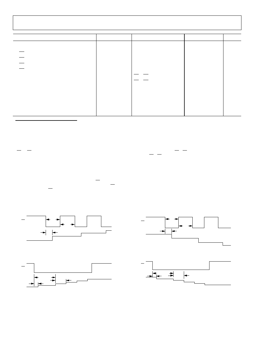
INTERFACE TIMING DIAGRAMS
04422-0-004
R
WB
PU
t
DB
t
PU
t
PU_REP
Figure 2. Increment R
WB
in Discrete Steps
04422-0-005
R
WB
PU
t
DB
t
AS
t
AS_START
Figure 3. Increment R
WB
in Autoscan Mode
04422-0-006
R
WB
PU
t
DB
t
PD
t
PD_REP
Figure 4. Decrement R
WB
in Discrete Steps
04422-0-007
R
WB
PD
t
DB
t
AS
t
AS_START
Figure 5. Decrement R
WB
in Autoscan Mode

AD5228
Rev. 0 | Page 5 of 20
ABSOLUTE MAXIMUM RATINGS
Table 3.
Parameter
Rating
V
DD
to GND
-0.3 V, +7 V
V
A
, V
B
, V
W
to GND
0 V, V
DD
PU, PD, PRE Voltage to GND
0 V, V
DD
Maximum Current
I
WB
, I
WA
Pulsed
±20 mA
I
WB
Continuous (R
WB
5 k, A open)
1
±1 mA
I
WA
Continuous (R
WA
5 k, B open)
1
±1
mA
I
AB
Continuous
(R
AB
= 10 k/50 k/100 k)
1
±500 µA/±100 µA/
±50 µA
Operating Temperature Range
-40∞C to +105∞C
Maximum Junction Temperature
(T
J
max)
150∞C
Storage Temperature
-65∞C to +150∞C
Lead Temperature
(Soldering, 10 s ≠ 30 s)
245∞C
Thermal Resistance
2
JA
230∞C/W
1
Maximum terminal current is bounded by the maximum applied voltage
across any two of the A, B, and W terminals at a given resistance, the
maximum current handling of the switches, and the maximum power
dissipation of the package. V
DD
= 5 V.
2
Package power dissipation = (T
J
max ≠ T
A
) /
JA
.
Stresses above those listed under Absolute Maximum Ratings
may cause permanent damage to the device. This is a stress
rating only and functional operation of the device at these or
any other conditions above those indicated in the operational
section of this specification is not implied. Exposure to absolute
maximum rating conditions for extended periods may affect
device reliability.
ESD CAUTION
ESD (electrostatic discharge) sensitive device. Electrostatic charges as high as 4000 V readily accumulate on
the human body and test equipment and can discharge without detection. Although this product features
proprietary ESD protection circuitry, permanent damage may occur on devices subjected to high energy
electrostatic discharges. Therefore, proper ESD precautions are recommended to avoid performance
degradation or loss of functionality.