 | ÐлекÑÑоннÑй компоненÑ: AD5241-10 | СкаÑаÑÑ:  PDF PDF  ZIP ZIP |
AD5241/42
REV. A
Information furnished by Analog Devices is believed to be accurate and
reliable. However, no responsibility is assumed by Analog Devices for its
use, nor for any infringements of patents or other rights of third parties that
may result from its use. No license is granted by implication or otherwise
under any patent or patent rights of Analog Devices.
a
AD5241/AD5242
One Technology Way, P.O. Box 9106, Norwood, MA 02062-9106, U.S.A.
Tel: 781/329-4700
www.analog.com
Fax: 781/326-8703
© Analog Devices, Inc., 2002
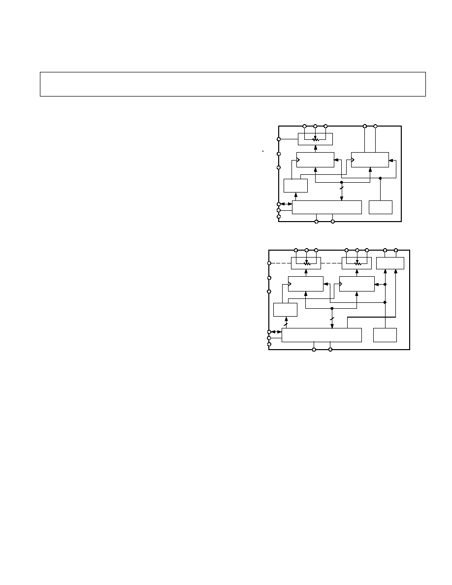
FUNCTIONAL BLOCK DIAGRAM
RDAC
REGISTER 1
ADDR
DECODE
8
PWR-ON
RESET
SERIAL INPUT REGISTER
AD5241
SHDN
V
DD
V
SS
SDA
SCL
GND
A
1
W
1
B
1
O
1
O
2
REGISTER 2
AD0
AD1
RDAC
REGISTER 1
ADDR
DECODE
8
PWR-ON
RESET
SERIAL INPUT REGISTER
AD5242
SHDN
V
DD
V
SS
SDA
SCL
GND
A
1
W
1
B
1
A
2
W
2
B
2
RDAC
REGISTER 2
O
2
O
1
REGISTER
1
AD0
AD1
FEATURES
256 Position
10 k , 100 k , 1 M
Low Tempco 30 ppm/ C
Internal Power ON Midscale Preset
Single Supply 2.7 V to 5.5 V or
Dual Supply 2.7 V for AC or Bipolar Operation
I
2
C-Compatible Interface with Reaback Capability
Extra Programmable Logic Outputs
APPLICATIONS
Multimedia, Video and Audio
Communications
Mechanical Potentiometer Replacement
Instrumentation: Gain, Offset Adjustment
Programmable Voltage-to-Current Conversion
Line Impedance Matching
GENERAL DESCRIPTION
The AD5241/AD5242 provides a single-/dual-channel, 256-
position digitally controlled variable resistor (VR) device. These
devices perform the same electronic adjustment function as a
potentiometer, trimmer or variable resistor. Each VR offers a
completely programmable value of resistance, between the A
terminal and the wiper, or the B terminal and the wiper. For
AD5242, the fixed A-to-B terminal resistance of 10 k
, 100 k
or 1 M
has a 1% channel-to-channel matching tolerance.
Nominal temperature coefficient of both parts is 30 ppm/
°C.
Wiper position programming defaults to midscale at system
power ON. Once powered, the VR wiper position is programmed
by an I
2
C-compatible 2-wire serial data interface. Both parts
have available two extra programmable logic outputs that
enable users to drive digital loads, logic gates, LED drivers, and
analog switches in their system.
The AD5241/AD5242 is available in surface-mount (SO-14/-16)
packages and, for ultracompact solutions, TSSOP-14/-16 pack-
ages. All parts are guaranteed to operate over the extended
industrial temperature range of 40
°C to +85°C. For 3-wire,
SPI-compatible interface applications, please refer to AD5200,
AD5201, AD5203, AD5204, AD5206, AD5231
*, AD5232*,
AD5235
*, AD7376, AD8400, AD8402, and AD8403 products.
I
2
C
®
-Compatible
256-Position Digital Potentiometers
*Nonvolatile digital potentiometer.
I
2
C is a registered trademark of Philips Corporation.

REV. A
2
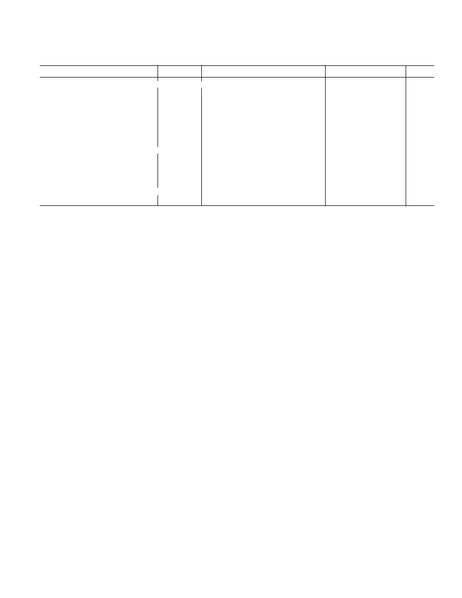
AD5241/AD5242SPECIFICATIONS
10 k , 100 k , 1 M VERSION
Parameter
Symbol
Conditions
Min
Typ
1
Max
Unit
DC CHARACTERISTICS, RHEOSTAT MODE (Specifications apply to all VRs.)
Resistor Differential Nonlinearity
2
R-DNL
R
WB
, V
A
= NC
1
±0.4
+1
LSB
Resistor Integral Nonlinearity
2
R-INL
R
WB
, V
A
= NC
2
±0.5
+2
LSB
Nominal Resistor Tolerance
R
T
A
= 25
°C, RAB = 10 k
30
+30
%
R
T
A
= 25
°C, RAB = 100 k/1 M
30
+50
%
Resistance Temperature Coefficient
R
AB
/
T
V
AB
= V
DD
, Wiper = No Connect
30
ppm/
°C
Wiper Resistance
R
W
I
W
= V
DD
/R, V
DD
= 3 V or 5 V
60
120
DC CHARACTERISTICS, POTENTIOMETER DIVIDER MODE (Specifications apply to all VRs.)
Resolution
N
8
Bits
Differential Nonlinearity
3
DNL
1
±0.4
+1
LSB
Integral Nonlinearity
3
INL
2
±0.5
+2
LSB
Voltage Divider Temperature Coefficient
V
W
/
T
Code = 80
H
5
ppm/
°C
Full-Scale Error
V
WFSE
Code = FF
H
1
0.5
0
LSB
Zero-Scale Error
V
WZSE
Code = 00
H
0
0.5
1
LSB
RESISTOR TERMINALS
Voltage Range
4
V
A, B, W
V
SS
V
DD
V
Capacitance
5
A, B
C
A, B
f = 1 MHz, Measured to GND, Code = 80
H
45
pF
Capacitance
5
W
C
W
f = 1 MHz, Measured to GND, Code = 80
H
60
pF
Common-Mode Leakage
I
CM
V
A
= V
B
= V
W
1
nA
DIGITAL INPUTS
Input Logic High (SDA and SCL)
V
IH
0.7 V
DD
V
DD
+ 0.5
V
Input Logic Low (SDA and SCL)
V
IL
0.5
+0.3 V
DD
V
Input Logic High (AD0 and AD1)
V
IH
V
DD
= 5 V
2.4
V
DD
V
Input Logic Low (AD0 and AD1)
V
IL
V
DD
= 5 V
0
0.8
V
Input Logic High
V
IH
V
DD
= 3 V
2.1
V
DD
V
Input Logic Low
V
IL
V
DD
= 3 V
0
0.6
V
Input Current
I
IL
V
IN
= 0 V or 5 V
1
µA
Input Capacitance
5
C
IL
3
pF
DIGITAL OUTPUT
V
OL
I
OL
= 3 mA
0.4
V
Output Logic Low (SDA)
V
OL
I
OL
= 6 mA
0.6
V
Output Logic Low (O
1
and O
2
)
V
OL
I
SINK
= 1.6 mA
0.4
V
Output Logic High (O
1
and O
2
)
V
OH
I
SOURCE
= 40
µA
4
V
Three-State Leakage Current (SDA)
I
OZ
V
IN
= 0 V or 5 V
±1
µA
Output Capacitance
5
C
OZ
3
8
pF
POWER SUPPLIES
Power Single-Supply Range
V
DD RANGE
V
SS
= 0 V
2.7
5.5
V
Power Dual-Supply Range
V
DD/SS RANGE
±2.3
±2.7
V
Positive Supply Current
I
DD
V
IH
= 5 V or V
IL
= 0 V
0.1
50
µA
Negative Supply Current
I
SS
V
SS
= 2.5 V, V
DD
= +2.5 V
+0.1
50
µA
Power Dissipation
6
P
DISS
V
IH
= 5 V or V
IL
= 0 V, V
DD
= 5 V
0.5
250
µW
Power Supply Sensitivity
PSS
0.01
+0.002 +0.01
%/%
DYNAMIC CHARACTERISTICS
5, 7, 8
Bandwidth 3 dB
BW_10 k
R
AB
= 10 k
, Code = 80
H
650
kHz
BW_100 k
R
AB
= 100 k
, Code = 80
H
69
kHz
BW_1 M
R
AB
= 1 M
, Code = 80
H
6
kHz
Total Harmonic Distortion
THD
W
V
A
= 1 V rms + 2 V dc,
0.005
%
V
B
= 2 V dc, f = 1 kHz
V
W
Settling Time
t
S
V
A
= V
DD
, V
B
= 0 V,
±1 LSB Error Band,
2
µs
R
AB
= 10 k
Resistor Noise Voltage
e
N_WB
R
WB
= 5 k
, f = 1 kHz
14
nV
Hz
(V
DD
= 3 V 10% or 5 V
10%, V
A
= +V
DD
, V
B
= 0 V, 40 C < T
A
< +85 C unless
otherwise noted.)
REV. A
3
AD5241/AD5242
Parameter
Symbol
Conditions
Min
Typ
1
Max
Unit
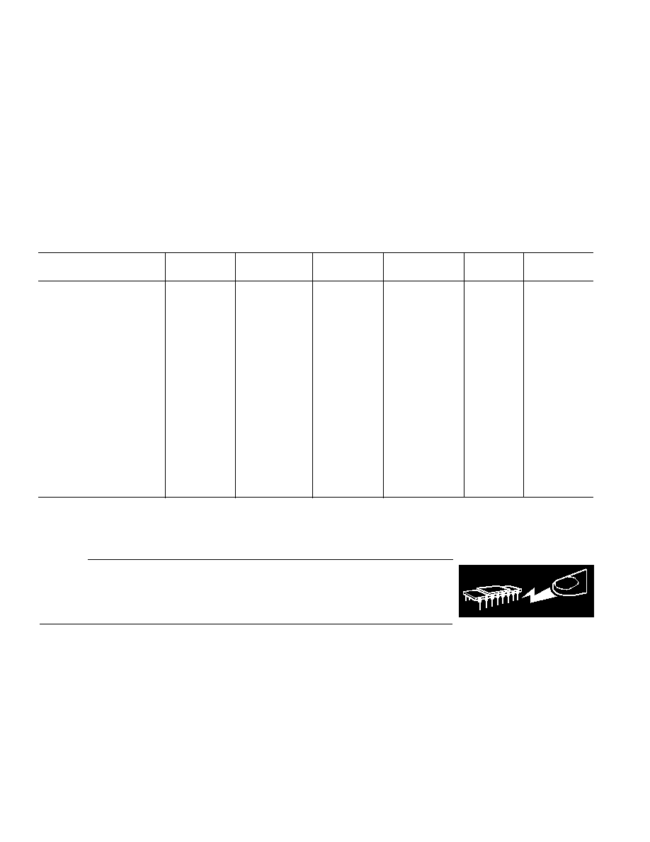
INTERFACE TIMING CHARACTERISTICS (Applies to all parts.
5, 9
)
SCL Clock Frequency
f
SCL
0
400
kHz
t
BUF
Bus Free Time Between
t
1
1.3
µs
STOP and START
t
HD; STA
Hold Time (Repeated START)
t
2
After this period the first clock
600
ns
pulse is generated.
t
LOW
Low Period of SCL Clock
t
3
1.3
µs
t
HIGH
High Period of SCL Clock
t
4
0.6
50
µs
t
SU; STA
Setup Time for START Condition
t
5
600
ns
t
HD; DAT
Data Hold Time
t
6
900
ns
t
SU; DAT
Data Setup Time
t
7
100
ns
t
R
Rise Time of Both
t
8
300
ns
SDA and SCL Signals
t
F
Fall Time of Both SDA and SCL Signals t
9
300
ns
t
SU; STO
Setup Time for STOP Condition
t
10
NOTES
1
Typicals represent average readings at 25
°C, V
DD
= 5 V.
2
Resistor position nonlinearity error R-INL is the deviation from an ideal value measured between the maximum resistance and the minimum resistance wiper posi-
tions. R-DNL measures the relative step change from ideal between successive tap positions. Parts are guaranteed monotonic. See Figure 10 test circuit.
3
INL and DNL are measured at V
W
with the RDAC configured as a potentiometer divider similar to a voltage output D/A converter. V
A
= V
DD
and V
B
= 0 V.
DNL specification limits of
±1 LSB maximum are Guaranteed Monotonic operating conditions. See Figure 9 test circuit.
4
Resistor terminals A, B, W have no limitations on polarity with respect to each other.
5
Guaranteed by design and not subject to production test.
6
P
DISS
is calculated from (I
DD
× V
DD
). CMOS logic level inputs result in minimum power dissipation.
7
Bandwidth, noise, and settling time are dependent on the terminal resistance value chosen. The lowest R value results in the fastest settling time and highest band-
width. The highest R value results in the minimum overall power consumption.
8
All dynamic characteristics use V
DD
= 5 V.
9
See timing diagram for location of measured values.
Specifications subject to change without notice.
REV. A
AD5241/AD5242
4
ABSOLUTE MAXIMUM RATINGS
*
(T
A
= 25
°C, unless otherwise noted)
V
DD
to GND . . . . . . . . . . . . . . . . . . . . . . . . . . . . . 0.3 , +7 V
V
SS
to GND . . . . . . . . . . . . . . . . . . . . . . . . . . . . . . . 0 V , 7 V
V
DD
to V
SS
. . . . . . . . . . . . . . . . . . . . . . . . . . . . . . . . . . . . . 7 V
V
A
, V
B
, V
W
to GND . . . . . . . . . . . . . . . . . . . . . . . . . . V
SS
, V
DD
A
X
B
X
, A
X
W
X
, B
X
W
X
at 10 k
in TSSOP-14 . . . ±5.0 mA
*
A
X
B
X
, A
X
W
X
, B
X
W
X
at 100 k
in TSSOP-14 . . ±1.5 mA
*
A
X
B
X
, A
X
W
X
, B
X
W
X
at 1 M
in TSSOP-14 . . . ±0.5 mA
*
Digital Input Voltage to GND . . . . . . . . . . . . . . . . . . 0 V, 7 V
Operating Temperature Range . . . . . . . . . . . 40
°C to +85°C
Thermal Resistance
JA
SOIC (SO-14) . . . . . . . . . . . . . . . . . . . . . . . . . . . 158
°C/W
SOIC (SO-16) . . . . . . . . . . . . . . . . . . . . . . . . . . . . 73
°C/W
TSSOP-14 . . . . . . . . . . . . . . . . . . . . . . . . . . . . . . 206
°C/W
TSSOP-16 . . . . . . . . . . . . . . . . . . . . . . . . . . . . . . 180
°C/W
Maximum Junction Temperature (T
J
max) . . . . . . . . . . 150
°C
Package Power Dissipation P
D
= (T
J
max T
A
)/
JA
Storage Temperature . . . . . . . . . . . . . . . . . . 65
°C to +150°C
Lead Temperatures
R-14, R-16, RU-14, RU-16 (Vapor Phase, 60 sec) . . 215
°C
R-14, R-16, RU-14, RU-16 (Infrared, 15 sec) . . . . . . 220
°C
*Max Current increases at lower resistance and different packages.
CAUTION
ESD (electrostatic discharge) sensitive device. Electrostatic charges as high as 4000 V readily
accumulate on the human body and test equipment and can discharge without detection. Although
the AD5241/AD5242 features proprietary ESD protection circuitry, permanent damage may occur
on devices subjected to high-energy electrostatic discharges. Therefore, proper ESD precautions
are recommended to avoid performance degradation or loss of functionality.
WARNING!
ESD SENSITIVE DEVICE
ORDERING GUIDE
Number of
End to End
Temperature
Package
Package
#Devices per
Model
Channels
R
AB
( )
Range ( C)
Description
Option
Container
AD5241BR10
1
10 k
40 to +85
SO-14
R-14
56
AD5241BR10-REEL7
1
10 k
40 to +85
SO-14
R-14
1000
AD5241BRU10-REEL7
1
10 k
40 to +85
TSSOP-14
RU-14
1000
AD5241BR100
1
100 k
40 to +85
SO-14
R-14
56
AD5241BR100-REEL7
1
100 k
40 to +85
SO-14
R-14
1000
AD5241BRU100-REEL7
1
100 k
40 to +85
TSSOP-14
RU-14
1000
AD5241BR1M
1
1 M
40 to +85
SO-14
R-14
56
AD5241BR1M-REEL7
1
1 M
40 to +85
SO-14
R-14
1000
AD5241BRU1M-REEL7
1
1 M
40 to +85
TSSOP-14
RU-14
1000
AD5242BR10
2
10 k
40 to +85
SO-16
R-16A
48
AD5242BR10-REEL7
2
10 k
40 to +85
SO-16
R-16A
1000
AD5242BRU10-REEL7
2
10 k
40 to +85
TSSOP-16
RU-16
1000
AD5242BR100
2
100 k
40 to +85
SO-16
R-16A
48
AD5242BR100-REEL7
2
100 k
40 to +85
SO-16
R-16A
1000
AD5242BRU100-REEL7
2
100 k
40 to +85
TSSOP-16
RU-16
1000
AD5242BR1M
2
1 M
40 to +85
SO-16
R-16A
48
AD5242BR1M-REEL7
2
1 M
40 to +85
SO-16
R-16A
1000
AD5242BRU1M-REEL7
2
1 M
40 to +85
TSSOP-16
RU-16
1000
NOTES
1. The AD5241/AD5242 die size is 69 mil
× 78 mil, 5,382 sq. mil. Contains 386 transistors for each channel. Patent Number 5495245 applies.
2. TSSOP packaged units are only available in 1,000-piece quantity Tape and Reel.
REV. A
5
AD5241/AD5242
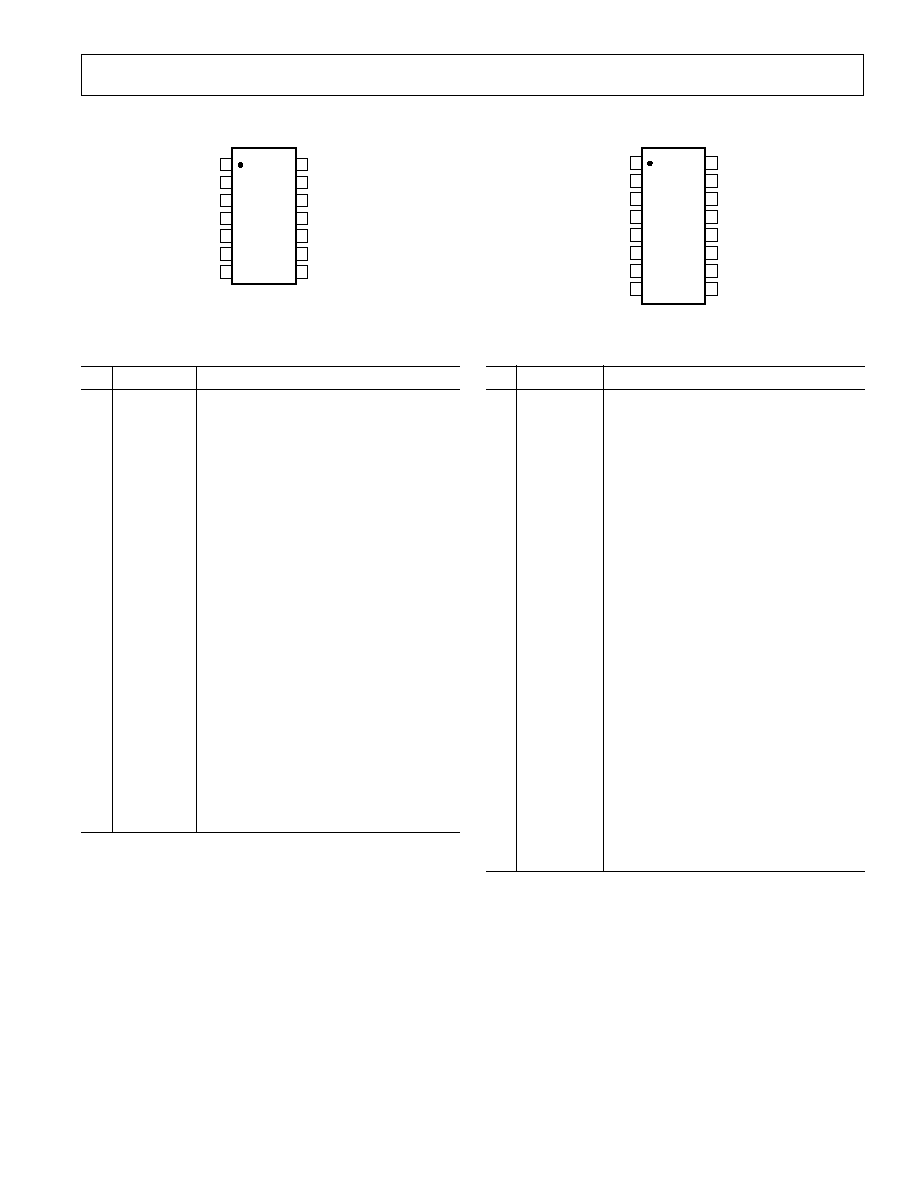
AD5242 PIN FUNCTION DESCRIPTIONS
Pin
Mnemonic
Description
1
O
1
Logic Output Terminal O
1
2
A
1
Resistor Terminal A
1
3
W
1
Wiper Terminal W
1
4
B
1
Resistor Terminal B
1
5
V
DD
Positive power supply, specified for opera-
tion from 2.2 V to 5.5 V.
6
SHDN
Active low, asynchronous connection of
the Wiper W to Terminal B, and open
circuit of Terminal A. RDAC register
contents unchanged.
SHDN should tie to
V
DD
if not used.
7
SCL
Serial Clock Input
8
SDA
Serial Data Input/Output
9
AD0
Programmable address bit for multiple
package decoding. Bits AD0 and AD1
provide four possible addresses.
10
AD1
Programmable address bit for multiple
package decoding. Bits AD0 and AD1
provide four possible addresses.
11
DGND
Common Ground
12
V
SS
Negative power supply, specified for
operation from 0 V to 2.7 V.
13
O
2
Logic Output Terminal O
2
14
B
2
Resistor Terminal B
2
15
W
2
Wiper Terminal W
2
16
A
2
Resistor Terminal A
2
AD5241 PIN CONFIGURATION
TOP VIEW
(Not to Scale)
14
13
12
11
10
9
8
1
2
3
4
5
6
7
NC = NO CONNECT
W
1
B
1
V
DD
SHDN
SCL
SDA
O
1
NC
O
2
V
SS
DGND
AD1
AD0
A
1
AD5241
AD5242 PIN CONFIGURATION
TOP VIEW
(Not to Scale)
16
15
14
13
12
11
10
9
1
2
3
4
5
6
7
8
O
1
A
1
W
1
B
1
V
DD
SHDN
SCL
SDA
A
2
W
2
B
2
O
2
V
SS
DGND
AD1
AD0
AD5242
AD5241 PIN FUNCTION DESCRIPTIONS
Pin
Mnemonic
Description
1
A
1
Resistor Terminal A
1
2
W
1
Wiper Terminal W
1
3
B
1
Resistor Terminal B
1
4
V
DD
Positive power supply, specified for opera-
tion from 2.2 V to 5.5 V.
5
SHDN
Active low, asynchronous connection of
the Wiper W to Terminal B, and open
circuit of Terminal A. RDAC register
contents unchanged.
SHDN should tie to
V
DD
if not used.
6
SCL
Serial Clock Input
7
SDA
Serial Data Input/Output
8
AD0
Programmable address bit for multiple
package decoding. Bits AD0 and AD1
provide four possible addresses.
9
AD1
Programmable address bit for multiple
package decoding. Bits AD0 and AD1
provide four possible addresses.
10
DGND
Common Ground
11
V
SS
Negative power supply, specified for
operation from 0 V to 2.7 V.
12
O
2
Logic Output Terminal O
2
13
NC
No Connect
14
O
1
Logic Output Terminal O
1
Document Outline
- FEATURES
- APPLICATIONS
- GENERAL DESCRIPTION
- FUNCTIONAL BLOCK DIAGRAM
- 10 k, 100 k, 1 M VERSION
- DC CHARACTERISTICS, RHEOSTAT MODE
- DC CHARACTERISTICS, POTENTIOMETER DIVIDER MODE
- DC CHARACTERISTICS, POTENTIOMETER DIVIDER MODE
- RESISTOR TERMINALS
- DIGITAL INPUTS
- DIGITAL OUTPUT
- POWER SUPPLIES
- DYNAMIC CHARACTERISTICS
- INTERFACE TIMING CHARACTERISTICS
- ABSOLUTE MAXIMUM RATINGS
- ORDERING GUIDE
- AD5241 PIN CONFIGURATION
- AD5241 PIN FUNCTION DESCRIPTIONS
- AD5242 PIN CONFIGURATION
- AD5242 PIN FUNCTION DESCRIPTIONS
- Typical Performance Characteristics
- OPERATION
- PROGRAMMING THE VARIABLE RESISTOR
- PROGRAMMING THE POTENTIOMETER DIVIDER
- DIGITAL INTERFACE
- MULTIPLE DEVICES ON ONE BUS
- LEVEL-SHIFT FOR BIDIRECTIONAL INTERFACE
- READBACK RDAC VALUE
- ADDITIONAL PROGRAMMABLE LOGIC OUTPUT
- Test Circuits
- DIGITAL POTENTIOMETER SELECTION GUIDE
- OUTLINE DIMENSIONS
- Revision History