Document Outline
- FEATURES
- APPLICATIONS
- GENERAL DESCRIPTION
- FUNCTIONAL BLOCK DIAGRAM
- ˛ˇ
- ˛ˇ
- ˛ˇ
- ˛ˇ
- ˛ˇ
- ˛ˇ
- ˛ˇ
- ˛ˇ
Quad 64-/256-Position I
2
C Nonvolatile
Memory Digital Potentiometers
AD5253/AD5254
Rev. 0
Information furnished by Analog Devices is believed to be accurate and reliable.
However, no responsibility is assumed by Analog Devices for its use, nor for any
infringements of patents or other rights of third parties that may result from its use.
Specifications subject to change without notice. No license is granted by implication
or otherwise under any patent or patent rights of Analog Devices. Trademarks and
registered trademarks are the property of their respective owners.
One Technology Way, P.O. Box 9106, Norwood, MA 02062-9106, U.S.A.
Tel: 781.329.4700
www.analog.com
Fax: 781.326.8703
© 2004 Analog Devices, Inc. All rights reserved.
FEATURES
AD5253: Quad 64-position resolution
AD5254: Quad 256-position resolution
1 k, 10 k, 50 k, 100 k
Nonvolatile memory
1
stores wiper settings with write
protection
Power-on refreshed to EEMEM settings in 300 µs typ
EEMEM rewrite time = 540 µs typ
Resistance tolerance stored in nonvolatile memory
12 extra bytes in EEMEM for user-defined information
I
2
CÆ compatible serial interface
Direct read/write accesses of RDAC
2
and EEMEM registers
Predefined linear increment/decrement commands
Predefined ±6 dB step change commands
Synchronous or asynchronous quad channel update
Wiper setting readback
4 MHz bandwidth--1 k version
Single supply 2.7 V to 5.5 V
Dual supply ±2.25 V to ±2.75 V
2 slave address decoding bits allow operation of 4 devices
100-year typical data retention, T
A
= 55∞C
Operating temperature: ≠40∞C to +85∞C
APPLICATIONS
Mechanical potentiometer replacement
Low resolution DAC replacement
RGB LED backlight control
White LED brightness adjustment
RF base station power amp bias control
Programmable gain and offset control
Programmable attenuators
Programmable voltage-to-current conversion
Programmable power supply
Programmable filters
Sensor calibrations
GENERAL DESCRIPTION
The AD5253/AD5254 are quad channel, I
2
C, nonvolatile mem-
ory, digitally controlled potentiometers with 64/256 positions,
respectively. These devices perform the same electronic adjust-
ment functions as mechanical potentiometers, trimmers, and
variable resistors.
The AD5253/AD5254's versatile programmability allows multi-
ple modes of operation, including read/write accesses in the
RDAC and EEMEM registers, increment/decrement of
resistance, resistance changes in ±6 dB scales, wiper setting
readback, and extra EEMEM for storing user-defined informa-
tion, such as memory data for other components, look-up table,
or system identification information.
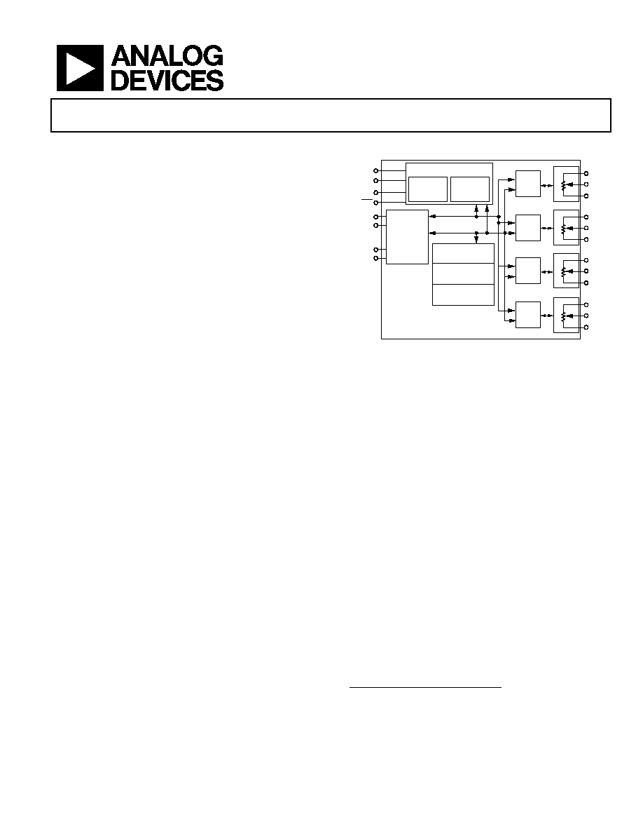
FUNCTIONAL BLOCK DIAGRAM
RDAC0
REGIS-
TER
RDAC1
REGIS-
TER
RDAC2
REGIS-
TER
RDAC3
REGIS-
TER
RDAC0
RDAC1
RDAC2
RDAC3
DATA
CONTROL
COMMAND
DECODE LOGIC
ADDRESS
DECODE LOGIC
CONTROL LOGIC
AD5253/AD5254
I
2
C
SERIAL
INTERFACE
V
DD
A0
W0
B0
A1
W1
B1
A2
W2
B2
A3
W3
B3
V
SS
DGND
SCL
SDA
AD0
AD1
WP
03824-0-001
EEMEM
POWER-ON
REFRESH
R
AB
TOL
RDAC EEMEM
Figure 1.
The AD5253/AD5254 allow the host I
2
C controllers to write any
of the 64-/256-step wiper settings in the RDAC registers and
store them in the EEMEM. Once the settings are stored, they are
restored automatically to the RDAC registers at system power-
on; the settings can also be restored dynamically.
The AD5253/AD5254 provide additional increment, decrement,
+6 dB step change, and ≠6 dB step change in synchronous or
asynchronous channel update modes. The increment and
decrement functions allow stepwise linear adjustments, while
±6 dB step changes are equivalent to doubling or halving the
RDAC wiper setting. These functions are useful for steep-slope
nonlinear adjustment applications such as white LED brightness
and audio volume control.
The AD5253/AD5254 have a patented resistance tolerance
storing function that allows the user to access the EEMEM and
obtain the absolute end-to-end resistance values of the RDACs
for precision applications.
The AD5253/AD5254 are available in TSSOP-20 packages in
1 k, 10 k, 50 k, and 100 k options. All parts are
guaranteed to operate over the ≠40∞C to +85∞C extended
industrial temperature range.
1
The terms nonvolatile memory and EEMEM are used interchangeably.
2
The terms digital potentiometer and RDAC are used interchangeably.

AD5253/AD5254
Rev. 0 | Page 2 of 28
TABLE OF CONTENTS
Electrical Characteristics ................................................................. 3
1 k Version.................................................................................. 3
10 k, 50 k, 100 k Versions ................................................... 5
Interface Timing Characteristics (All Parts)............................. 7
Absolute Maximum Ratings............................................................ 8
ESD Caution.................................................................................. 8
Pin Configuration and Functional Descriptions.......................... 9
Typical Performance Characteristics ........................................... 10
I
2
C Interface..................................................................................... 14
I
2
C Interface General Description............................................ 14
I
2
C Interface Detail Description ............................................... 15
I
2
C Compatible 2-Wire Serial Bus............................................ 19
Theory of Operation ...................................................................... 20
Linear Increment and Decrement Commands ...................... 20
±6 dB Adjustments (Doubling/Halving Wiper Setting)........ 20
Digital Input/Output Configuration........................................ 21
Multiple Devices On One Bus .................................................. 21
Terminal Voltage Operation Range ......................................... 22
Power-Up and Power-Down Sequences.................................. 22
Layout and Power Supply Biasing ............................................ 22
Digital Potentiometer Operation ............................................. 23
Programmable Rheostat Operation......................................... 23
Programmable Potentiometer Operation ............................... 24
Applications..................................................................................... 25
RGB LED LCD Backlight Controller....................................... 25
Outline Dimensions ....................................................................... 27
Ordering Guide .......................................................................... 27
REVISION HISTORY
Revision 0: Initial Version

AD5253/AD5254
Rev. 0 | Page 3 of 28
ELECTRICAL CHARACTERISTICS
1 k VERSION
V
DD
= +3 V ± 10% or +5 V ± 10%, V
SS
= 0 V or V
DD
/V
SS
= ±2.5 V ± 10%, V
A
= +V
DD
, V
B
= 0 V, ≠40∞C < T
A
< +85∞C, unless otherwise noted.
Table 1.
Parameter Symbol
Conditions
Min
Typ
1
Max Unit
DC CHARACTERISTICS--RHEOSTAT MODE
Resolution N
AD5253/AD5254
6/8
Bits
Resistor Differential Nonlinearity
2
R-DNL R
WB
, R
WA
= NC, V
DD
= 5.5V, AD5253
≠0.5
±0.2
+0.5
LSB
R
WB
, R
WA
= NC, V
DD
= 5.5V, AD5254
≠1
±0.25
+1
LSB
R
WB
, R
WA
= NC, V
DD
= 2.7V, AD5253
≠0.75
±0.3
+0.75
LSB
R
WB
, R
WA
= NC, V
DD
= 2.7V, AD5254
≠1.5
±0.3
+1.5
LSB
Resistor Nonlinearity
2
R-INL R
WB
, R
WA
= NC, V
DD
= 5.5V, AD5253
≠0.5
±0.2
+0.5
LSB
R
WB
, R
WA
= NC, V
DD
= 5.5V, AD5254
≠2
±0.5
+2
LSB
R
WB
, R
WA
= NC, V
DD
= 2.7V, AD5253
≠1
+2.5
+4
LSB
R
WB
, R
WA
= NC, V
DD
= 2.7V, AD5254
≠2
+9
+14
LSB
Nominal Resistor Tolerance
R
AB
/R
AB
T
A
= 25∞C
≠30
+30
%
Resistance Temperature
Coefficient (R
AB
/R
AB
) ◊ 10
6
/T
650
ppm/∞C
Wiper Resistance
R
W
I
W
= 1 V/R, V
DD
= 5 V
75
130
I
W
= 1 V/R, V
DD
= 3 V
200
300
Channel Resistance Matching
R
AB1
/R
AB2
0.15
%
DC CHARACTERISTICS--POTENTIOMETER DIVIDER MODE
Differential Nonlinearity
3
DNL
AD5253
≠0.5 ±0.1 +0.5 LSB
AD5254 ≠1
±0.25
+1
LSB
Integral Nonlinearity
3
INL
AD5253
≠0.5 ±0.2 +0.5 LSB
AD5254 ≠2
±0.5
+2
LSB
Voltage Divider Temperature
Coefficient (V
W
/V
W
) ◊ 10
6
/T
Code = Half scale
25
ppm/∞C
Full-Scale Error
V
WFSE
Code = Full scale, V
DD
= 5.5 V, AD5253
≠5
≠3
0
LSB
Code = Full scale, V
DD
= 5.5 V, AD5254
≠16
≠11
0
LSB
Code = Full scale, V
DD
= 2.7 V, AD5253
≠6
≠4
0
LSB
Code = Full scale, V
DD
= 2.7 V, AD5254
≠23
≠16
0
LSB
Zero-Scale Error
V
WZSE
Code = Zero scale, V
DD
= 5.5 V, AD5253
0
3
5
LSB
Code = Zero scale, V
DD
= 5.5 V, AD5254
0
11
16
LSB
Code = Zero scale, V
DD
= 2.7 V, AD5253
0
4
6
LSB
Code = Zero scale, V
DD
= 2.7 V, AD5254
0
15
20
LSB
RESISTOR
TERMINALS
Voltage Range
4
V
A
, V
B
, V
W
V
SS
V
DD
V
Capacitance
5
Ax, Bx
C
A
, C
B
f = 1 kHz, measured to GND,
Code = Half scale
85
pF
Capacitance
5
Wx
C
W
f = 1 kHz, measured to GND,
Code = Half scale
95
pF
Common-Mode Leakage
Current I
CM
V
A
= V
B
= V
DD
/2
0.01
1
µA
DIGITAL INPUTS AND OUTPUTS
Input Logic High
V
IH
V
DD
= 5 V, V
SS
= 0 V
2.4
V
V
DD
/V
SS
= +2.7 V/0 V or V
DD
/V
SS
= ±2.5 V
2.1
V
Input Logic Low
V
IL
V
DD
=5 V, V
SS
= 0 V
0.8
V
V
DD
/V
SS
= +2.7 V/0 V or V
DD
/V
SS
= ±2.5 V
0.6
V
Output Logic High (SDA)
V
OH
R
PULL-UP
= 2.2 k to V
DD
= 5 V, V
SS
= 0 V
4.9
V
Output Logic Low (SDA)
V
OL
R
PULL-UP
= 2.2 k to V
DD
=5 V, V
SS
= 0 V
0.4
V
WP Leakage Current
I
WP
WP = V
DD
5
µA

AD5253/AD5254
Rev. 0 | Page 4 of 28
Parameter Symbol
Conditions
Min
Typ
1
Max Unit
DIGITAL INPUTS AND OUTPUTS (continued)
A0 Leakage Current
I
A0
A0 = GND
3
µA
Input Leakage Current (Other
than WP and A0)
I
I
V
IN
= 0 V or V
DD
±1
µA
Input Capacitance
5
C
I
5
pF
POWER
SUPPLIES
Single-Supply Power Range
V
DD
V
SS
= 0 V
2.7
5.5
V
Dual-Supply Power Range
V
DD
/V
SS
±2.25
±2.75
V
Positive Supply Current
I
DD
V
IH
= V
DD
or V
IL
= GND
5
15
µA
Negative Supply Current
I
SS
V
IH
= V
DD
or V
IL
= GND, V
DD
= +2.5 V,
V
SS
= ≠2.5 V
≠5
≠15
µA
EEMEM Data Storing Mode
Current I
DD_STORE
V
IH
= V
DD
or V
IL
= GND
35
mA
EEMEM Data Restoring Mode
Current
6
I
DD_RESTORE
V
IH
= V
DD
or V
IL
= GND
2.5
mA
Power Dissipation
7
P
DISS
V
IH
= V
DD
= 5 V or V
IL
= GND
0.075
mW
Power Supply Sensitivity
PSS
V
DD
= 5 V ±10%
-0.025
0.01
0.025
%/%
V
DD
= 3 V ±10%
≠0.04
0.02
0.04
%/%
DYNAMIC CHARACTERISTICS
5, 8
Bandwidth ≠3 dB
BW
R
AB
= 1 k
4
MHz
Total Harmonic Distortion
THD
V
A
=1 V rms, V
B
= 0 V, f = 1 kHz
0.05
%
V
W
Settling Time
t
S
V
A
= V
DD
, V
B
= 0 V
0.2
µs
Resistor Noise Voltage
e
N_WB
R
WB
= 500 , f = 1 kHz. Thermal noise
only.
3
nV/Hz
Digital Crosstalk
C
T
V
A
= V
DD
, V
B
= 0 V, measure V
W
with
adjacent RDAC making full-scale change
≠80
dB
Analog Coupling
C
AT
Signal input at A0 and measure the
output at W1, f = 1 kHz
≠72
dB

AD5253/AD5254
Rev. 0 | Page 5 of 28
10 k, 50 k, 100 k VERSIONS
V
DD
= +3 V± 10% or +5 V± 10%, V
SS
= 0 V or V
DD
/V
SS
= ±2.5 V ± 10%, V
A
= +V
DD
, V
B
= 0 V, ≠40∞C < T
A
< +85∞C, unless otherwise noted.
Table 2.
Parameter Symbol
Conditions
Min
Typ
1
Max
Unit
DC CHARACTERISTICS--RHEOSTAT MODE
Resolution N AD5253/AD5254
6/8
Bits
Resistor Differential
Nonlinearity
2
R-DNL R
WB
, R
WA
= NC, AD5253
-0.75
±0.1
+0.75
LSB
R
WB
, R
WA
= NC, AD5254
-1
±0.25
+1
LSB
Resistor Nonlinearity
2
R-INL
R
WB
, R
WA
= NC, AD5253
-0.75
±0.25
+0.75
LSB
R
WB
, R
WA
= NC, AD5254
-2.5
±1
+2.5
LSB
Nominal Resistor Tolerance
R
AB
/R
AB
T
A
= 25∞C
-20
+20
%
Resistance Temperature
Coefficient
(R
AB
/R
AB
) ◊ 10
6
/T
650 ppm/∞C
Wiper Resistance
R
W
I
W
= 1 V/R, V
DD
= 5 V
75
130
I
W
= 1 V/R, V
DD
= 3 V
200
300
Channel Resistance
Matching R
AB1
/R
AB2
R
AB
= 10 k, 50 k
0.15
%
R
AB
= 100 k
0.05
%
DC CHARACTERISTICS--POTENTIOMETER DIVIDER MODE
Differential Nonlinearity
3
DNL
AD5253
-0.5 ±0.1
+0.5 LSB
AD5254
-1 ±0.3 +1 LSB
Integral Nonlinearity
3
INL
AD5253
-0.5 ±0.15 +0.5 LSB
AD5254
-1.5 ±0.5
+1.5 LSB
Voltage Divider
Temperature Coefficient
(V
W
/V
W
) ◊ 10
6
/T
Code = Half scale
15
ppm/∞C
Full-Scale Error
V
WFSE
Code = Full scale, AD5253
-1
-0.3
0
LSB
Code = Full scale, AD5254
-3
-1
0
LSB
Zero-Scale Error
V
WZSE
Code = Zero scale, AD5253
0
0.3
1
LSB
Code = Zero scale, AD5254
0
1.2
3
LSB
RESISTOR
TERMINALS
Voltage Range
4
V
A
, V
B
, V
W
V
SS
V
DD
V
Capacitance
5
Ax, Bx
C
A
, C
B
f = 1 kHz, measured to GND,
Code = Half scale
85 pF
Capacitance
5
Wx
C
W
f = 1 kHz, measured to GND,
Code = Half scale
95 pF
Common-Mode Leakage
Current
6
I
CM
V
A
= V
B
= V
DD
/2
0.01
1
µA
DIGITAL INPUTS AND OUTPUTS
Input Logic High
V
IH
V
DD
= 5 V, V
SS
= 0 V
2.4
V
V
DD
/V
SS
= +2.7 V/0 V or V
DD
/V
SS
= ±2.5 V
2.1
V
Input Logic Low
V
IL
V
DD
= 5 V, V
SS
= 0 V
0.8
V
V
DD
/V
SS
= +2.7 V/0 V or V
DD
/V
SS
= ±2.5 V
0.6
V
Output Logic High (SDA)
V
OH
R
PULL-UP
= 2.2 k to V
DD
= 5 V, V
SS
= 0 V
4.9
V
Output Logic Low (SDA)
V
OL
R
PULL-UP
= 2.2 k to V
DD
= 5 V, V
SS
= 0 V
0.4
V
WP Leakage Current
I
WP
WP = V
DD
5
µA
A0 Leakage Current
I
A0
A0 = GND
3
µA
Input Leakage Current
(Other than WP and A0)
I
I
V
IN
= 0 V or V
DD
±1
µA
Input Capacitance
5
C
I
5 pF
POWER
SUPPLIES
Single-Supply Power Range
V
DD
V
SS
= 0 V
2.7
5.5
V
Dual-Supply Power Range
V
DD
/V
SS
±2.25
±2.75 V
Positive Supply Current
I
DD
V
IH
= V
DD
or V
IL
= GND
5
15
µA