Äîêóìåíòàöèÿ è îïèñàíèÿ www.docs.chipfind.ru
3-Channel Digital Potentiometer with
Nonvolatile Memory
AD5255
Rev. 0
Information furnished by Analog Devices is believed to be accurate and reliable.
However, no responsibility is assumed by Analog Devices for its use, nor for any
infringements of patents or other rights of third parties that may result from its use.
Specifications subject to change without notice. No license is granted by implication
or otherwise under any patent or patent rights of Analog Devices. Trademarks and
registered trademarks are the property of their respective owners.
One Technology Way, P.O. Box 9106, Norwood, MA 02062-9106, U.S.A.
Tel: 781.329.4700
www.analog.com
Fax: 781.326.8703
© 2004 Analog Devices, Inc. All rights reserved.
FEATURES
3 channels:
Dual 512-position
Single 128-position
25 k or 250 k full-scale resistance
Low temperature coefficient:
Potentiometer divider 15 ppm/°C
Rheostat mode 35 ppm/
°C
Nonvolatile memory retains wiper settings
Permanent memory write protection
Linear increment/decrement
±6 dB increment/decrement
I
2
C-compatible serial interface
2.7 V to 5.5 V single-supply operation
±2.25 V to ±2.75 V dual-supply operation
Power-on reset time
256 bytes general-purpose user EEPROM
11 bytes RDAC user EEPROM
GBIC and SFP compliant EEPROM
100-year typical data retention at T
A
= 55°C
APPLICATIONS
Mechanical potentiometer replacement
RGB LED backlight control
White LED brightness adjustment
Programmable gain and offset control
Programmable filters
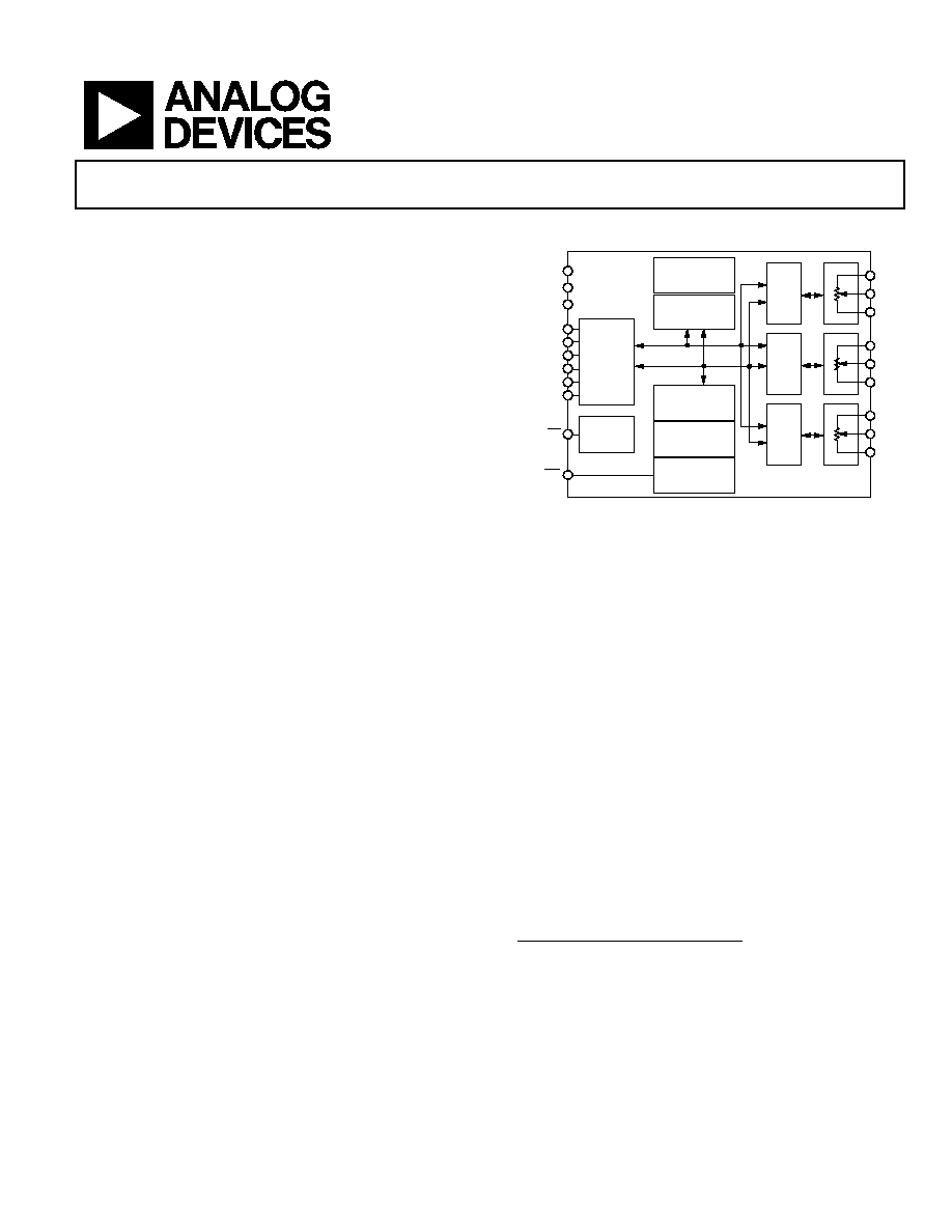
FUNCTIONAL BLOCK DIAGRAM
A0
W0
B0
A1
W1
B1
A2
W2
B2
A0
W0
B0
A0
W0
B0
A1
W1
B1
A1
W1
B1
A2
W2
B2
A2
W2
B2
RDAC0
RDAC0
REGIST
ER
RDAC1
REGIST
ER
RDAC2
REGIST
ER
9 BIT
RDAC1
9 BIT
RDAC2
7 BIT
DATA
CONTROL
COMMAND
DECODE
LOGIC
ADDRESS
DECODE
LOGIC
DECODE
LOGIC
POWER-ON
RESET
I
2
C
SERIAL
INTERFACE
32 BYTES
RDAC
EEPROM
256 BYTES
USER
EEPROM
V
DD
V
SS
GND
SCL
SDA
A0_RDAC
A1_RDAC
A0_E
A1_E
RS
WP
04555-0-001
Figure 1.
GENERAL DESCRIPTION
The AD5255 provides dual 512-position and a single
128-position digitally controlled variable resistors
1
(VR) in a
TSSOP package. This device performs the same electronic
adjustment function as a potentiometer, trimmer, or variable
resistor. Each VR offers a completely programmable value of
resistance between the A terminal and the wiper or the B
terminal and the wiper. The fixed A-to-B terminal resistance of
25 k or 250 k has a 1% channel-to-channel matching
tolerance and a nominal temperature coefficient of 35 ppm/°C.
Wiper position programming, EEPROM
2
reading, and EEPROM
writing is conducted via the standard 2-wire I
2
C interface. Pre-
vious/default wiper position settings can be stored in memory,
and refreshed upon system power-up.
Additional features of the AD5255 include preprogrammed
linear and logarithmic increment/decrement wiper changing.
The actual resistor tolerances are stored in EEPROM so that the
actual end-to-end resistance is known, which is valuable for
calibration in precision applications.
The AD5255 is available in a 24-lead TSSOP package. All parts
are guaranteed to operate over the extended industrial tempera-
ture range of -40°C to +85°C.
1
The terms programmable resistor, variable resistor, RDAC, and digital
potentiometer are used interchangeably.
2
The terms nonvolatile memory, EEMEM, and EEPROM are used
interchangeably.

AD5255
Rev. 0 | Page 2 of 20
TABLE OF CONTENTS
Electrical Characteristics ................................................................. 3
Electrical Characteristics ................................................................. 5
Absolute Maximum Ratings............................................................ 6
ESD Caution.................................................................................. 6
Pin Configuration and Function Descriptions............................. 7
Typical Performance Characteristics ............................................. 8
Interface Descriptions .................................................................... 10
I
2
C Interface ................................................................................ 10
EEPROM Interface..................................................................... 11
RDAC I
2
C Interface.................................................................... 12
Theory of Operation ...................................................................... 15
Linear Increment and Decrement Commands ...................... 15
Logarithmic Taper Mode Adjustment (±6 dB/step) .............. 15
Using Additional Internal Nonvolatile EEPROM .................. 16
Digital Input/Output Configuration........................................ 16
Multiple Devices on One Bus ................................................... 16
Level Shift for Bidirectional Communication ........................ 16
Terminal Voltage Operation Range ......................................... 16
Power-Up Sequence ................................................................... 17
Layout and Power Supply Biasing ............................................ 17
RDAC Structure.......................................................................... 17
Calculating the Programmable Resistance ............................. 17
Programming the Potentiometer Divider............................... 18
Applications..................................................................................... 19
Laser Diode Driver (LDD) Calibration................................... 19
Outline Dimensions ....................................................................... 20
Ordering Guide .......................................................................... 20
REVISION HISTORY
7/04--Revision 0: Initial Version

AD5255
Rev. 0 | Page 3 of 20
ELECTRICAL CHARACTERISTICS
Single supply: V
DD
= 2.7 V to 5.5 V and -40°C < T
A
< +85°C, unless otherwise noted.
Dual supply: V
DD
= +2.25 V or +2.75 V, V
SS
= -2.25 V or -2.75 V and -40°C < T
A
< +85°C, unless otherwise noted.
Table 1.
Parameter Symbol
Conditions
Min
Typ
1
Max Unit
DC CHARACTERISTICS,
RHEOSTAT MODE
Resistor Differential Nonlinearity
2
R-DNL R
WB
, 7-bit channel
-0.75
+0.75 LSB
R
WB
, 9-bit channels
-2.5
+2.5 LSB
Resistor Integral Nonlinearity
2
R-INL R
WB
, 7-bit channel
-0.5
+0.5 LSB
R-INL R
WB
, 9-bit channels, V
DD
= 5.5 V
-2.0
+2.0 LSB
R-INL R
WB
, 9-bit channels, V
DD
= 2.7 V
-4.0
+4.0 LSB
Resistance Temperature Coefficent
(R
WB
/R
WB
)/T × 10
6
35
ppm/°C
Wiper Resistance
R
W
V
DD
= 5 V, I
W
= 1 V/R
WB
100 150
V
DD
= 3 V, I
W
= 1 V/R
WB
250 400
Channel Resistance Matching
R
AB1
/R
AB2
Ch 1 and 2 R
WB
, Dx = 0x1FF
0.1
%
Nominal Resistor Tolerance
R
AB
/R
AB
Dx = 0x3FF
-15
+15 %
DC CHARACTERISTICS,
POTENTIOMETER DIVIDER MODE
Differential Nonlinearity
3
DNL 7-bit
channel
-0.5
+0.5 LSB
DNL 9-bit
channels
-2.0
+2.0 LSB
Integral Nonlinearity
3
INL 7-bit
channel
-0.5
+0.5 LSB
INL 9-bit
channels
-2.0
+2.0 LSB
Voltage Divider Temperature
Coefficent
(V
W
/V
W
)/T × 10
6
Code = half-scale
15
ppm/°C
Full-Scale Error
V
WFSE
7-bit channel/9-bit channel,
code = full-scale
-1/-2.75
0/0 LSB
Zero-Scale Error
V
WZSE
7-bit channel/9-bit channel,
code = zero-scale
0/0
1/2.0 LSB
RESISTOR
TERMINALS
Terminal Voltage Range
4
V
A, B, W
V
SS
V
DD
V
Capacitance
5
Ax, Bx
C
A,B
f = 1 kHz, measured to GND,
code = half-scale
85
pF
Capacitance
5
Wx
C
W
f = 1 kHz, measured to GND,
code = half-scale
95
pF
Common-Mode Leakage Current
5, 8
I
CM
V
W
= V
DD
/2
0.01 1
µA
DIGITAL INPUTS AND OUTPUTS
Input Logic High
V
IH
V
DD
= 5 V, V
SS
= 0 V
2.4
V
V
DD
/V
SS
= +2.7 V/0 V or
V
DD
/V
SS
= ±2.5 V
2.1
V
Input Logic Low
V
IL
V
DD
= 5 V, V
SS
= 0 V
0.8 V
V
DD
/V
SS
= +2.7 V/0 V or
V
DD
/V
SS
= ±2.5 V
0.6 V
Output Logic High (SDA)
V
OH
R
PULL-UP
= 2.2 k to V
DD
= 5 V,
V
SS
= 0 V
4.9
V
Output Logic Low
V
OL
R
PULL-UP
= 2.2 k to V
DD
= 5 V,
V
SS
= 0 V
0.4 V
WP Leakage Current
I
WP
WP = V
DD
9 µA
A0 Leakage Current
I
A0
A0 = GND
3 µA
AD5255
Rev. 0 | Page 4 of 20
Parameter Symbol
Conditions
Min
Typ
1
Max Unit
Input Leakage Current (Excluding WP
and A0)
I
I
V
IN
= 0 V or V
DD
±1 µA
Input Capacitance
5
C
I
5
pF
POWER
SUPPLIES
Single-Supply Power Range
V
DD
V
SS
= 0 V
2.7
5.5 V
Dual-Supply Power Range
V
DD
/V
SS
±2.25
±2.75 V
Positive Supply Current
I
DD
V
IH
= V
DD
or V
IL
= GND, V
SS
= 0 V
5 15
µA
Negative Supply Current
I
SS
V
IH
= V
DD
or V
IL
= GND,
V
DD
= 2.5 V, V
SS
= -2.5 V
-5 -15
µA
EEMEM Data Storing Mode Current
I
DD_STORE
V
IH
= V
DD
or V
IL
= GND
35
mA
EEMEM Data Restoring Mode Current
I
DD_RESTORE
V
IH
= V
DD
or V
IL
= GND
2.5
mA
Power Dissipation
6
P
DISS
V
IH
= V
DD
= 5 V or V
IL
= GND
25 75 µW
Power Supply Sensitivity
5
P
SS
V
DD
= 5 V ± 10%
0.01 0.025
%/%
See the footnotes after Table 2.
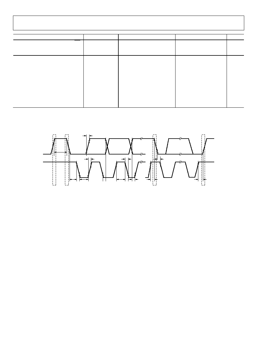
04555-0-015
SDA
SCL
P
S
S
P
t
1
t
2
t
3
t
8
t
8
t
9
t
4
t
5
t
7
t
10
t
6
Figure 2. I
2
C Timing Diagram

AD5255
Rev. 0 | Page 5 of 20
ELECTRICAL CHARACTERISTICS
Single Supply: V
DD
= 3 V to 5.5 V and -40°C < T
A
< +85°C, unless otherwise noted.
Dual Supply: V
DD
= +2.25 V or +2.75 V , V
SS
= -2.25 V or -2.75 V and -40°C < T
A
< + 85°C, unless otherwise noted.
Table 2.
Parameter Symbol
Conditions
Min
Typ
1
Max Unit
DYNAMIC CHARACTERISTICS
5, 7
Bandwidth -3 dB
BW
V
DD
/V
SS
= ±2.5 V, R
AB
= 25 k/250 k
125/12
kHz
Total Harmonic Distortion
THD
W
V
A
= 1 V rms, V
B
= 0 V, f = 1 kHz
0.05
%
V
W
Settling Time
t
S
V
A
= V
DD
, V
B
= 0 V,
V
W
= 0.50% error band,
code 0x000 to 0x100, R
AB
= 25 k/250 k
4/36
µs
Resistor Noise Spectral Density
e
N_WB
R
AB
= 25 k/250 k, T
A
= 25°C
14/45
nVHz
Digital Crosstalk
C
T
V
A
= V
DD
, V
B
= 0 V, measure VW with
adjacent RDAC making full-scale
change
-80 dB
Analog Crosstalk
C
AT
Signal input at A0 and measure output
at W1, f = 1 kHz
-72 dB
INTERFACE TIMING CHARACTERISTICS
(apply to all parts) (Notes
8, 9
)
SCL Clock Frequency
f
SCL
400
kHz
t
BUF
Bus Free Time between Stop and
Start
t
1
1.3
µs
t
HD;STA
Hold Time (Repeated Start)
t
2
After this period the first clock pulse is
generated
600
ns
t
LOW
Low Period of SCL Clock
t
3
1.3
µs
t
HIGH
High Period of SCL Clock
t
4
0.6
50 µs
t
SU;STA
Setup Time for Start Condition
t
5
600
ns
t
HD;DAT
Data Hold Time
t
6
900
ns
t
SU;DAT
Data Setup Time
t
7
100
ns
t
R
Rise Time of Both SDA and SCL
Signals
t
8
300
ns
t
F
Fall Time of Both SDA and SCL
Signals
t
9
300
ns
t
SU;STO
Setup Time for Stop Condition
t
10
600
ns
EEMEM Data Storing Time
t
EEMEM_STORE
26 ms
EEMEM Data Restoring Time at
Power-On
t
EEMEM_RESTORE1
360 µs
EEMEM Data Restoring Time on
Restore
t
EEMEM_RESTORE2
360 µs
Command or Reset Operation
EEMEM Data Rewritable Time
t
EEMEM_REWRITE
540
µs
FLASH/EE MEMORY RELIABILITY
Endurance
10
100
kcycles
Data Retention
11
55°C
100 years
1
Typical represent average readings at 25°C, V
DD
= 5 V.
2
Resistor position nonlinearity error R-INL is the deviation from an ideal value measured between the maximum resistance and the minimum resistance wiper
positions. R-DNL measures the relative step change from ideal between successive tap positions.
3
INL and DNL are measured at V
W
with the RDAC configured as a potentiometer divider similar to a voltage output D/A converter. V
A
= V
DD
and V
B
= 0 V.
4
Resistor Terminals A, B, W have no limitations on polarity with respect to each other.
5
Guaranteed by design and not subject to production test.
6
P
DISS
is calculated from (I
DD
× V
DD
). CMOS logic level inputs result in minimum power dissipation.
7
All dynamic characteristics use V
DD
= 5 V.
8
Bandwidth, noise, and settling time are dependent on the terminal resistance value chosen. The lowest R value results in the fastest settling time and highest
bandwidth. The highest R value results in the minimum overall power consumption.
9
See the timing diagram for location of measured values.
10
Endurance is qualified to 100,000 cycles as per JEDEC Std. 22 method A117 and measured at -40°C, +25°C, and +85°C, typical endurance at 25°C is 700,000 cycles.
11
Retention lifetime equivalent at junction temperature (T
J
) = 55°C as per JEDEC Std. 22, Method A117. Retention lifetime based on an activation energy of 0.6eV
derates with junction temperature.
Document Outline
- FEATURES
- APPLICATIONS
- GENERAL DESCRIPTION
- FUNCTIONAL BLOCK DIAGRAM
- þÿ
- þÿ
- þÿ
- þÿ
- þÿ
- þÿ
- þÿ
- þÿ
- þÿ