Äîêóìåíòàöèÿ è îïèñàíèÿ www.docs.chipfind.ru
Nonvolatile, I
2
C-Compatible
64-Position, Digital Potentiometer
AD5258
Rev. 0
Information furnished by Analog Devices is believed to be accurate and reliable.
However, no responsibility is assumed by Analog Devices for its use, nor for any
infringements of patents or other rights of third parties that may result from its use.
Specifications subject to change without notice. No license is granted by implication
or otherwise under any patent or patent rights of Analog Devices. Trademarks and
registered trademarks are the property of their respective owners.
One Technology Way, P.O. Box 9106, Norwood, MA 02062-9106, U.S.A.
Tel: 781.329.4700
www.analog.com
Fax: 781.326.8703
© 2005 Analog Devices, Inc. All rights reserved.
FEATURES
Nonvolatile memory maintains wiper settings
64-position
Compact MSOP-10 (3 mm × 4.9 mm) package
I
2
C®-compatible interface
V
LOGIC
pin provides increased interface flexibility
End-to-end resistance 1 k, 10 k, 50 k, 100 k
Resistance tolerance stored in EEPROM (0.1% accuracy)
Power-on EEPROM refresh time <1 ms
Software write protect command
Three-state Address Decode Pins AD0 and AD1 allow
9 packages per bus
100-year typical data retention at 55°C
Wide operating temperature -40°C
to +85°C
3 V to 5 V single supply
APPLICATIONS
LCD panel V
COM
adjustment
LCD panel brightness and contrast control
Mechanical potentiometer replacement in new designs
Programmable power supplies
RF amplifier biasing
Automotive electronics adjustment
Gain control and offset adjustment
Fiber to the home systems
Electronics level settings
GENERAL DESCRIPTION
The AD5258 provides a compact, nonvolatile 3 mm × 4.9 mm
packaged solution for 64-position adjustment applications.
These devices perform the same electronic adjustment function
as mechanical potentiometers
1
or variable resistors, but with
enhanced resolution and solid-state reliability.
The wiper settings are controllable through an I
2
C-compatible
digital interface that is also used to read back the wiper register
and EEPROM content. Resistor tolerance is also stored within
EEPROM providing an end-to-end tolerance accuracy of 0.1%.
There is also a software write protection function that ensures
data cannot be written to the EEPROM register.
A separate V
LOGIC
pin delivers increased interface flexibility. For
users who need multiple parts on one bus, Address Bit AD0 and
Address Bit AD1 allow up to nine devices on the same bus.
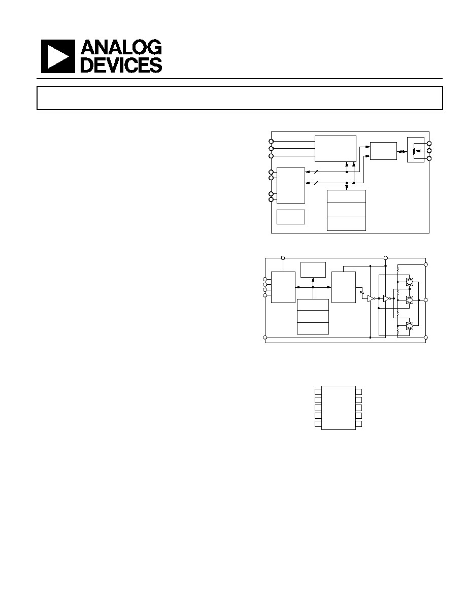
FUNCTIONAL BLOCK DIAGRAMS
05029-
001
RDAC
REGISTER
RDAC
DATA
CONTROL
COMMAND
DECODE LOGIC
ADDRESS
DECODE LOGIC
CONTROL LOGIC
AD5258
I
2
C
SERIAL
INTERFACE
POWER-
ON RESET
A
W
B
SCL
SDA
AD0
AD1
V
DD
V
LOGIC
GND
RDAC
EEPROM
6
6
Figure 1. Block Diagram
05029-
003
COMMAND
DECODE LOGIC
ADDRESS
DECODE LOGIC
CONTROL
LOGIC
SCL
SDA
AD0
AD1
GND
EEPROM
I
2
C
SERIAL
INTERFACE
RDAC
REGISTER
AND
LEVEL
SHIFTER
A
W
B
V
LOGIC
V
DD
Figure 2. Block Diagram Showing Level Shifters
CONNECTION DIAGRAM
05029-002
AD5258
TOP VIEW
(Not to Scale)
W
1
AD0
2
AD1
3
SDA
4
SCL
5
A
B
V
DD
GND
V
LOGIC
10
9
8
7
6
Figure 3. Pinout
1
The terms digital potentiometer, VR (variable resistor), and RDAC are used
interchangeably.

AD5258
Rev. 0 | Page 2 of 24
TABLE OF CONTENTS
Specifications..................................................................................... 3
Electrical Characteristics............................................................. 3
Timing Characteristics ................................................................ 5
Absolute Maximum Ratings............................................................ 6
ESD Caution.................................................................................. 6
Pin Configuration and Function Descriptions............................. 7
Typical Performance Characteristics ............................................. 8
Test Circuits..................................................................................... 13
Theory of Operation ...................................................................... 14
Programming the Variable Resistor......................................... 14
Programming the Potentiometer Divider ............................... 14
I
2
C Interface..................................................................................... 15
I
2
C Byte Formats ............................................................................. 16
Generic Interface ........................................................................ 16
Write Modes................................................................................ 17
Read Modes................................................................................. 17
Store/Restore Modes .................................................................. 17
Tolerance Readback Modes ...................................................... 18
ESD Protection of Digital Pins and Resistor Terminals........ 19
Power-Up Sequence ................................................................... 19
Layout and Power Supply Bypassing ....................................... 19
Multiple Devices on One Bus ................................................... 19
Evaluation Board ........................................................................ 19
Display Applications ...................................................................... 20
Circuitry ...................................................................................... 20
Outline Dimensions ....................................................................... 21
Ordering Guide .......................................................................... 21
REVISION HISTORY
3/05--Revision 0: Initial Version

AD5258
Rev. 0 | Page 3 of 24
SPECIFICATIONS
ELECTRICAL CHARACTERISTICS
V
DD
= V
LOGIC
= 5 V ± 10%, or 3 V ± 10%; V
A
= V
DD
; V
B
= 0 V; -40°C < T
A
< +85°C, unless otherwise noted.
Table 1.
Parameter Symbol
Conditions
Min
Typ
1
Max Unit
DC CHARACTERISTICS: RHEOSTAT MODE
Resistor Differential Nonlinearity
R-DNL
R
WB
, V
A
= no connect
LSB
1 k
-1.5
±0.3
+1.5
10 k/50 k/100 k
-0.25
±0.1
+0.25
Resistor Integral Nonlinearity
R-INL
R
WB
, V
A
= no connect
LSB
1 k
-5
±0.5
+5
10 k/100 k
-0.5
±0.1
+0.5
50 k
-0.25
±0.1
+0.25
Nominal Resistor Tolerance
T
A
= 25°C, V
DD
= 5.5 V
1 k
R
AB
0.9
1.5
k
10 k/50 k/100 k
R
AB
-30
+30
%
Resistance Temperature Coefficient
(R
AB
× 10
6
)/(R
AB
× T)
Code = 0x00/0x20
200/15
ppm/°C
Total Wiper Resistance
R
WB
Code = 0x00
75
350
DC CHARACTERISTICS:
POTENTIOMETER DIVIDER MODE
Differential Nonlinearity
DNL
LSB
1 k
-1
±0.3
+1
10 k/50 k/100 k
-0.25
±0.1
+0.25
Integral Nonlinearity
INL
LSB
1 k
-1
±0.3
+1
10 k/50 k/100 k
-0.25
±0.1
+0.25
Full-Scale Error
V
WFSE
Code = 0x3F
LSB
1 k
-6
-3
0
10 k
-1
-0.3
0
50 k/100 k
-1
-0.1
0
Zero-Scale Error
V
WZSE
Code = 0x00
LSB
1 k
0
3
5
10 k
0
0.3
1
50 k/100 k
0
0.1
0.5
Voltage Divider Temperature
Coefficient
(V
W
× 10
6
)/(V
W
× T)
Code = 0x00/0x20
120/15
ppm/°C
RESISTOR TERMINALS
Voltage Range
V
A, B, W
GND
V
DD
V
Capacitance A, B
C
A, B
f = 1 MHz, measured to GND,
code = 0x20
45
pF
Capacitance W
C
W
f = 1 MHz, measured to GND,
code = 0x20
60
pF
Common-Mode Leakage
I
CM
V
A
= V
B
= V
DD
/2
10
nA
DIGITAL INPUTS AND OUTPUTS
Input Logic High
V
IH
0.7 × V
L
V
L
+ 0.5
V
Input Logic Low
V
IL
-0.5
0.3
×
V
L
V
Leakage Current
I
IL
µA
SDA, AD0, AD1
V
IN
= 0 V or 5 V
0.01
±1
SCL Logic High
V
IN
= 0 V
-2.5
-1.4
+1
SCL Logic Low
V
IN
= 5 V
0.01
±1
Input Capacitance
C
IL
5
pF

AD5258
Rev. 0 | Page 4 of 24
Parameter Symbol
Conditions
Min
Typ
1
Max Unit
POWER SUPPLIES
Power Supply Range
V
DD
2.7
5.5
V
Positive Supply Current
I
DD
0.5
2
µA
Logic Supply
V
LOGIC
2.7
5.5
V
Logic Supply Current
I
LOGIC
V
IH
= 5 V or V
IL
= 0 V
3.5
6
µA
Programming Mode Current (EEPROM)
I
LOGIC(PROG)
V
IH
= 5 V or V
IL
= 0 V
35
mA
Power Dissipation
P
DISS
V
IH
= 5 V or V
IL
= 0 V, V
DD
= 5 V
20
40
µW
Power Supply Rejection Ratio
PSRR
V
DD
= +5 V ± 10%, Code = 0x20
±0.01
±0.06
%/%
DYNAMIC CHARACTERISTICS
Bandwidth -3 dB
BW
Code = 0x20
R
AB
= 1 k
18000
kHz
R
AB
= 10 k
1000
kHz
R
AB
= 50 k
190
kHz
R
AB
= 100 k
100
kHz
Total Harmonic Distortion
THD
W
R
AB
= 10 k, V
A
= 1 V rms, V
B
= 0,
f = 1 kHz
0.1
%
V
W
Settling Time
t
S
R
AB
= 10 k, V
AB
= 5 V,
±1 LSB error band
500
ns
Resistor Noise Voltage Density
e
N_WB
R
WB
= 5 k, f = 1 kHz
9
nV/Hz
1
Typical values represent average readings at 25°C and V = 5 V.
DD
AD5258
Rev. 0 | Page 5 of 24
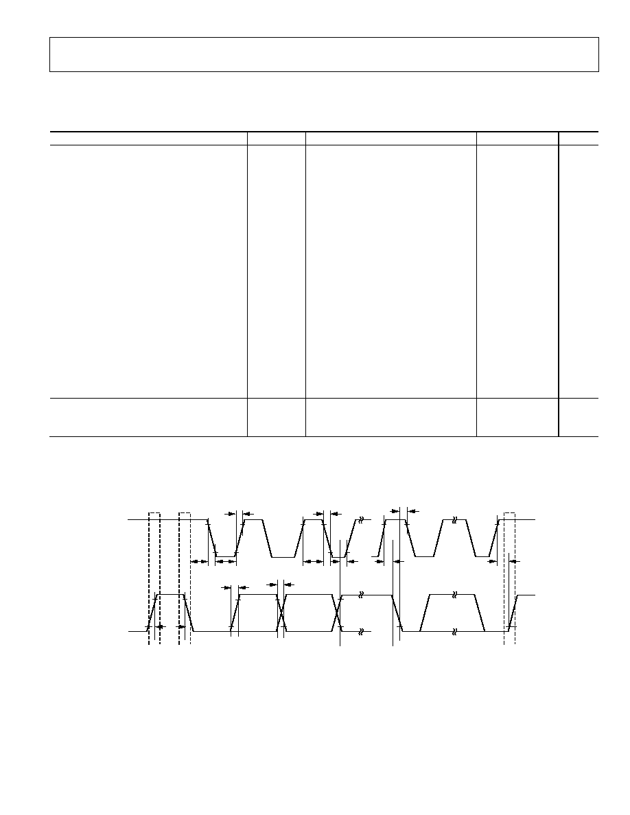
TIMING CHARACTERISTICS
V
DD
= V
LOGIC
= 5 V ± 10%, or 3 V ± 10%; V
A
= V
DD
; V
B
= 0 V; -40°C < T
A
< +85°C, unless otherwise noted.
Table 2.
Parameter
Symbol
Conditions
Min Typ Max Unit
I
2
C INTERFACE TIMING CHARACTERISTICS
SCL Clock Frequency
f
SCL
0
400
kHz
t
BUF
Bus Free Time between STOP and START
t
1
1.3
µs
t
HD;STA
Hold Time (Repeated START)
t
2
After this period, the first clock pulse is
generated.
0.6
µs
t
LOW
Low Period of SCL Clock
t
3
1.3
µs
t
HIGH
High Period of SCL Clock
t
4
0.6
µs
t
SU;STA
Setup Time for Repeated START
Condition
t
5
0.6
µs
t
HD;DAT
Data Hold Time
t
6
0
0.9
µs
t
SU;DAT
Data Setup Time
t
7
100
ns
t
F
Fall Time of Both SDA and SCL Signals
t
8
300
ns
t
R
Rise Time of Both SDA and SCL Signals
t
9
300
ns
t
SU;STO
Setup Time for STOP Condition
t
10
0.6
µs
EEPROM Data Storing Time
t
EEMEM_STORE
26
ms
EEPROM Data Restoring Time at Power On
1
t
EEMEM_RESTORE1
V
DD
rise time dependant. Measure
without decoupling capacitors at V
DD
and
GND.
300
µs
EEPROM Data Restoring Time upon Restore
Command
1
t
EEMEM_RESTORE2
V
DD
= 5 V.
300
µs
EEPROM Data Rewritable Time
2
t
EEMEM_REWRITE
540
µs
FLASH/EE MEMORY RELIABILITY
Endurance
3
100
700
kCycles
Data Retention
4
100
Years
1
During power-up, the output is momentarily preset to midscale before restoring EEPROM content.
2
Delay time after power-on PRESET prior to writing new EEPROM data.
3
Endurance is qualified to 100,000 cycles per JEDEC Std. 22 method A117, and is measured at 40°C, +25°C, and +85°C; typical endurance at +25°C is 700,000 cycles.
4
Retention lifetime equivalent at junction temperature (T
J
) = 55°C per JEDEC Std. 22, Method A117. Retention lifetime based on an activation energy of 0.6eV derates
with junction temperature.
05029-004
t
1
SCL
SDA
P
S
P
t
3
t
2
t
8
t
9
t
8
t
9
t
4
t
5
t
7
t
6
t
10
Figure 4. I
2
C Interface Timing Diagram
Document Outline
- FEATURES
- APPLICATIONS
- GENERAL DESCRIPTION
- FUNCTIONAL BLOCK DIAGRAMS
- CONNECTION DIAGRAM
- þÿ
- þÿ
- þÿ
- þÿ
- þÿ
- þÿ
- þÿ
- þÿ
- þÿ
- þÿ