Äîêóìåíòàöèÿ è îïèñàíèÿ www.docs.chipfind.ru
PRELIMINARY TECHNICAL DATA
a
Quad +15V 256-Step DigiPOTs
with Pin Selectable SPI / I
2
C Digital Interface
Preliminary Technical Data
AD5263
08 AUG '02, REV PrD
Information furnished by Analog Devices is believed to be accurate and reliable. However, no
responsibility is assumed by Analog Devices for its use; nor for any infringements of patents or
other rights of third parties which may result from its use. No license is granted by implication
or otherwise under any patent or patent rights of Analog Devices.
One Technology Way, P.O. Box 9106,
Norwood, MA 02062-9106 U
.
S
.
A
.
Tel: 781/329-4700
World Wide Web Site: http://www.analog.com
Fax: 781/326-8703
© Analog Devices, Inc., 2002
FEATURES
256 Position
4-Channel (Independently Programmable)
20k, 50k, 200k Ohms
Low Temperature Coefficient 50ppm/
o
C
Selectable Digital Interface (3-Wire SPI Compatible or 2-Wire I
2
C
Compatible Serial Data Input)
Operating temperature range -40 to 125ºC
+5 to +15V Single-Supply; ±5V Dual-Supply Operation
APPLICATIONS
Mechanical Potentiometer Replacement
Optical Network Laser LED Adjust
Instrumentation: Gain, Offset Adjustment
Stereo Channel Audio Level Control
Automotive Electronics Adjustment
Programmable Voltage to Current Conversion
Programmable Filters, Delays, Time Constants
Line Impedance Matching
Low Resolution DAC Replacement
GENERAL DESCRIPTION
The AD5263 is the industry first quad channel, 256 position,
digital potentiometer
1
selectable digital interface. These devices
perform the same electronic adjustment function as mechanical
potentiometers or variable resistor with enhanced resolution, solid-
state reliability, and superior low temperature coefficient
performance. Each Channel of the AD5263 contains a fixed resistor
with a wiper contact that taps the fixed resistor value at a point
determined by a digital code loaded into the 3 wire SPI or 2-wire
I
2
C compatible serial-input register. The resistance between the
wiper and either end point of the fixed resistor varies linearly with
respect to the digital code transferred into the RDAC latch
1
. The
variable resistor offers a completely programmable value of
resistance, between the A terminal and the wiper or the B terminal
and the wiper. The fixed A to B terminal resistance of 20k, 50k or
200k
has a nominal temperature coefficient of 50 ppm/°C. Unlike
majority of the digital potentiometers in the market, these devices
can operate up to 15V or ±5V provided proper supply voltages are
furnished.
The AD5263 are available in thin narrow body TSSOP-24. All
parts are guaranteed to operate over the extended automotive
temperature range of -40°C to +125°C.
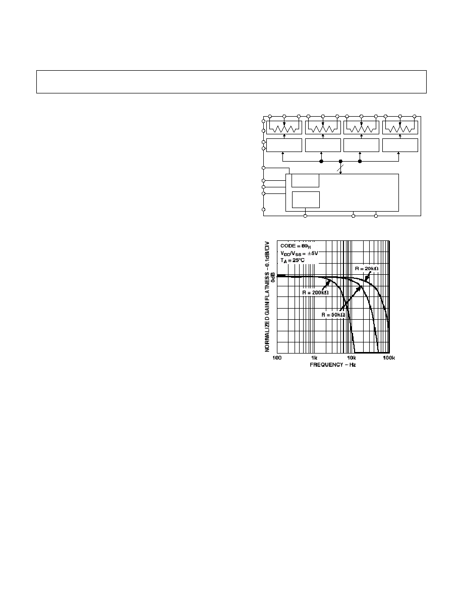
Functional Block Diagram
A1
W1
B1
A2
W2
B2
A3
W3
B3
A4
W4
B4
RDAC 1
REGISTER
RDAC 2
REGISTER
RDAC 3
REGISTER
RDAC 4
REGISTER
SERIAL INPUT
REGISTER
8
CLK /SCL
SDI / SDA
CS / AD0
V
L
GND
DIS
SDO / O1
NC / O2
V
DD
SHDN
RESB / AD1
V
SS
SPI / I
2
C
SELECT
LOGIC
ADDRESS
DECODER
AD5263
Figure 1 Normalized Gain Flatness Versus Frequency.

PRELIMINARY TECHNICAL DATA
Quad +15V Digital Potentiometers
AD5263
08 AUG '02, REV PrD
- 2 -
ELECTRICAL CHARACTERISTICS 20K, 50K, 200K OHM VERSION
(V
DD
=
+
5V
,
V
SS
= -5V, V
L
= +5V
,
V
A
= +V
DD
, V
B
= 0V, -40°C < T
A
< +125°C unless otherwise noted.)
Parameter Symbol
Conditions
Min
Typ
1
Max
Units
DC CHARACTERISTICS RHEOSTAT MODE Specifications apply to all VRs
Resistor Differential NL
2
R-DNL
R
WB
, V
A
=NC -1
±1/4
+1
LSB
Resistor Nonlinearity
2
R-INL
R
WB
, V
A
=NC -2
±1/2
+2
LSB
Nominal resistor tolerance
3
R
AB
T
A
= 25°C
-30
30
%
Resistance Temperature Coefficient
R
AB
/
T
Wiper = No Connect
30
ppm/°C
Wiper Resistance
R
W
I
W
= 1 V/R
AB
, V
DD
= +5V
50
100
DC CHARACTERISTICS POTENTIOMETER DIVIDER MODE Specifications apply to all VRs
Resolution N
8
Bits
Differential Nonlinearity
4
DNL
1 ±1/4 +1
LSB
Integral Nonlinearity
4
INL
2 ±1/2 +2
LSB
Voltage Divider Temperature Coefficient
V
W
/
T
Code = 40
H
5
ppm/°C
Full-Scale Error
V
WFSE
Code = FF
H
2
-1
+0
LSB
Zero-Scale Error
V
WZSE
Code = 00
H
0
+1
+2
LSB
RESISTOR TERMINALS
Voltage Range
5
V
A,B,W
V
SS
V
DD
V
Capacitance
6
Ax, Bx
C
A,B
f = 1 MHz, measured to GND, Code = 40
H
TBD
pF
Capacitance
6
Wx
C
W
f = 1 MHz, measured to GND, Code = 40
H
TBD
pF
Common-Mode Leakage
I
CM
V
A
=V
B
= V
DD
/ 2
1
nA
DIGITAL INPUTS
Input Logic High
V
IH
2.4
V
Input Logic Low
V
IL
0.8
V
Input Logic High
V
IH
V
L
= +3V, V
SS
= 0V
2.1
V
Input Logic Low
V
IL
V
L
= +3V, V
SS
= 0V
0.6
V
Input Current
I
IL
V
IN
= 0V or +5V
±1
µA
Input Capacitance
6
C
IL
5
pF
DIGITAL Output
O1, O2
V
OH
I
OH
=0.4mA
2.4
5.5
V
O1, O2
V
OL
I
OL
=-1.6mA
0
0.4
V
SDA V
OL
I
OL
= -6mA
0.6
V
SDA V
OL
I
OL
= -3mA
0.4
V
Three-State Leakage Current
I
OZ
V
IN
= 0V or +5V
±1
µA
Output Capacitance
6
C
OZ
3 8
pF
POWER SUPPLIES
Logic Supply
V
L
2.7
5.5
V
Power Single-Supply Range
V
DD RANGE
V
SS
= 0V
5
16.5
V
Power Dual-Supply Range
V
DD/SS RANGE
±4.5 ±5.5
V
Logic Supply Current
I
L
V
L
= +5V
60
µA
Positive Supply Current
I
DD
V
IH
= +5V or V
IL
= 0V
1
µA
Negative Supply Current
I
SS
V
SS
= -5V
1
µA
Power Dissipation
9
P
DISS
V
IH
= +5V or V
IL
= 0V, V
DD
= +5V, V
SS
= -5V
0.6
mW
Power Supply Sensitivity
PSS
V
DD
= +5V ±10%
0.0002
0.005
%/%
DYNAMIC CHARACTERISTICS
6, 10
Bandwidth 3dB
BW_20K
R
AB
= 20K
400
KHz
Total Harmonic Distortion
THD
W
V
A
=1Vrms, V
B
= 0V, f=1KHz, R
AB
= 20K
0.008
%
V
W
Settling Time
t
S
V
A
= 10V, V
B
=0V, ±1 LSB error band
2
µs
Resistor Noise Voltage
e
N_WB
R
WB
= 10K
, f = 1KHz, RS = 0
9
nV
Hz

PRELIMINARY TECHNICAL DATA
Quad +15V Digital Potentiometers
AD5263
08 AUG '02, REV PrD
- 3 -
ELECTRICAL CHARACTERISTICS 20K, 50K, 200K OHM VERSION
(V
DD
=
+
5V
,
V
SS
= -5V, V
L
= +5V,
V
A
= +V
DD
, V
B
= 0V, -40°C < T
A
< +125°C unless otherwise noted.)
Parameter Symbol
Conditions
Min
Typ
1
Max
Units
SPI (DIS='0') INTERFACE TIMING CHARACTERISTICS applies to all parts (Notes 6,12)
Input Clock Pulse Width
t
CH
,t
CL
Clock level high or low
50
ns
Data Setup Time
t
DS
20
ns
Data Hold Time
t
DH
20
ns
CLK to SDO Propagation Delay
13
t
PD
R
L
= 1K
, C
L
< 20pF
1
150
ns
CS Setup Time
t
CSS
20
ns
CS High Pulse Width
t
CSW
40
ns
Reset Pulse Width
t
RS
90
ns
CLK Fall to
CS Rise Hold Time
t
CSH
0
ns
CS Rise to Clock Rise Setup
t
CS1
10
ns
I
2
C (DIS='1') INTERFACE TIMING CHARACTERISTICS applies to all parts(Notes 6,12)
SCL Clock Frequency
f
SCL
0 400
KHz
t
BUF
Bus free time between
STOP & START
t
1
1.3
µs
t
HD;STA
Hold Time (repeated START)
t
2
After this period the first clock pulse is generated
0.6
µs
t
LOW
Low Period of SCL Clock
t
3
1.3
µs
t
HIGH
High Period of SCL Clock
t
4
0.6
µs
t
SU;STA
Setup Time For START Condition t
5
0.6
µs
t
HD;DAT
Data Hold Time
t
6
0 0.9
µs
t
SU;DAT
Data Setup Time
t
7
100
ns
t
F
Fall Time of both SDA & SCL signals
t
8
300
ns
t
R
Rise Time of both SDA & SCL signals
t
9
300
ns
t
SU;STO
Setup time for STOP Condition
t
10
0.6
µs
NOTES:
1.
Typicals represent average readings at +25°C and V
DD
= +5V, V
SS
= -5V.
2.
Resistor position nonlinearity error R-INL is the deviation from an ideal value measured between the maximum resistance and the minimum resistance wiper positions. R-DNL measures the
relative step change from ideal between successive tap positions. Parts are guaranteed monotonic. I
W
= V
DD
/R for both V
DD
=+5V, V
SS
=-5V.
3. V
AB
= V
DD
, Wiper (V
W
) = No connect
4.
INL and DNL are measured at V
W
with the RDAC configured as a potentiometer divider similar to a voltage output D/A converter. VA = V
DD
and V
B
= 0V.
DNL specification limits of ±1LSB maximum are Guaranteed Monotonic operating conditions.
5.
Resistor terminals A, B, W have no limitations on polarity with respect to each other.
6.
Guaranteed by design and not subject to production test.
7.
Measured at the Ax terminals. All Ax terminals are open circuited in shutdown mode.
8.
Worst case supply current consumed when input all logic-input levels set at 2.4V, standard characteristic of CMOS logic.
9. PDISS is calculated from (IDD x VDD). CMOS logic level inputs result in minimum power dissipation.
10.
All dynamic characteristics use V
DD
= +5V, V
SS
= -5V, V
L
= +5V
.
11.
Measured at a VW pin where an adjacent VW pin is making a full-scale voltage change.
12.
See timing diagram for location of measured values. All input control voltages are specified with tR=tF=2ns(10% to 90% of +3V) and timed from a voltage level of 1.5V. Switching characteristics
are measured using V
L
= +5V.
13.
Propagation delay depends on value of V
DD
, R
L
, and C
L
see applications text.
14.
The AD5260/AD5262 contains 1,968 transistors. Die Size: 89mil x 105mil, 9,345sq. mil.
PRELIMINARY TECHNICAL DATA
Quad +15V Digital Potentiometers
AD5263
08 AUG '02, REV PrD
- 4 -
ABSOLUTE MAXIMUM RATINGS (T
A
= +25°C, unless
otherwise noted)
V
DD
to GND ........................................................... -0.3, +15V
V
SS
to GND................................................................. 0V, -7V
V
DD
to V
SS
....................................................................... +15V
V
A
, V
B
, V
W
to GND................................................. V
SS
, V
DD
A
X
B
X
, A
X
W
X
, B
X
W
X
Intermittent
2
...................................................±20mA
Continuous ......................................................±2mA
Digital Inputs & Output Voltage to GND .................. 0V, +7V
Operating Temperature Range .........................-40°C to +85°C
Maximum Junction Temperature (T
J MAX
) .................. +150°C
Storage Temperature ......................................-65°C to +150°C
Lead Temperature (Soldering, 10 sec) ......................... +300°C
Vapor Phase (60 sec)....................................... +215 °C
Infrared (15 sec)...............................................+220 °C
Thermal Resistance
*
JA,
TSSOP-24........................................................143°C/W
*
Package Power Dissipation = (TJMAX - TA) /
JA
NOTES
1. Stresses above those listed under Absolute Maximum Ratings may
cause permanent damage to the device. This is a stress rating; functional
operation of the device at these or any other conditions above those
listed in the operational sections of this specification is not implied.
Exposure to absolute maximum rating conditions for extended periods
may affect device reliability.
2. Maximum terminal current is bounded by the maximum current
handling of the switches, maximum power dissipation of the package,
and maximum applied voltage across any two of the A, B, and W
terminals at a given resistance.
ORDERING GUIDE
Model R
AB
(k
)
Temp Package
Description
Package
Option
# Parts per
Container
Top Mark*
AD5263BRU20 20
-40/+125°C
TSSOP-24
RU-24
62
AD5263B20
AD5263BRU20-REEL7 20
-40/+125°C
TSSOP-24
RU-24 1,000
AD5263B20
AD5263BRU50 50
-40/+125°C
TSSOP-24
RU-24
62
AD5263B50
AD5263BRU50-REEL7 50
-40/+125°C
TSSOP-24
RU-24 1,000
AD5263B50
AD5263BRU200 200
-40/+125°C
TSSOP-24
RU-24
62
AD5263B200
AD5263BRU200-REEL7 200 -40/+125°C
TSSOP-24
RU-24 1,000 AD5263B200
*Line 1 contains part number, line 2 branding containing differentiating detail by part type and ADI logo symbol, line 3 contains date code YWW.
CAUTION
ESD (electrostatic discharge) sensitive device. Electrostatic charges as high as 4000 V readily
accumulate on the human body and test equipment and can discharge without detection. Although the
AD5263 features proprietary ESD protection circuitry, permanent damage may occur on devices
subjected to high-energy electrostatic discharges. Therefore, proper ESD precautions are recommended
to avoid performance degradation or loss of functionality.
PRELIMINARY TECHNICAL DATA
Quad +15V Digital Potentiometers
AD5263
08 AUG '02, REV PrD
- 5 -
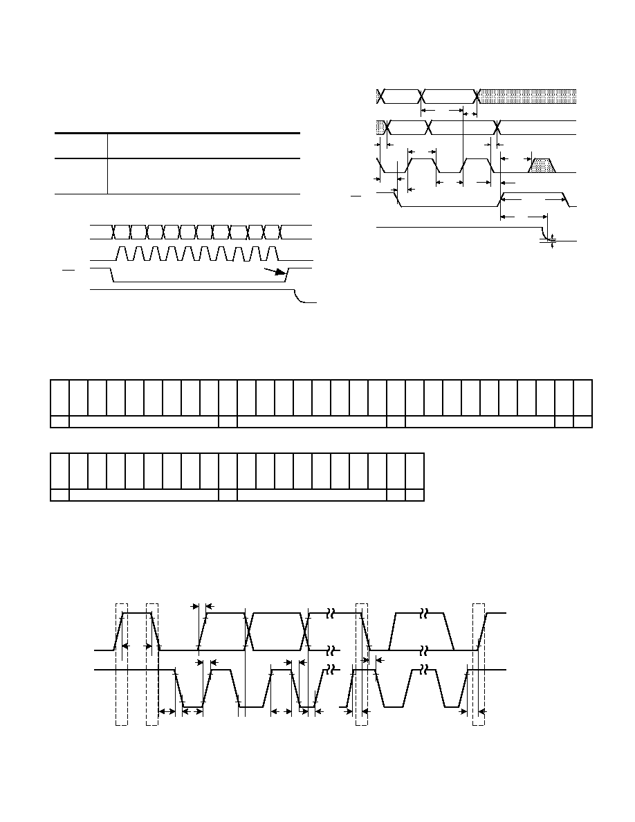
SPI Compatible Digital Interface (DIS='0')
TABLE IA: SPI 10-Bit Serial-Data Word
Format
ADDR DATA
B9
B8 B7 B6 B5 B4 B3 B2 B1 B0
A1
A0 D7 D6 D5 D4 D3 D2 D1 D0
MSB
LSB
2
9
2
7
2
0
A
1 A
0
D
7
D
6
D
5
D
4
D
3
D
1
D0
S
D
I
C
L
K
CS
V
O
U
T
0
1
0
1
0
1
0
1
D
2
RDAC REGISTER LOAD
Figure 1A. SPI Timing Diagram
1
0
1
0
1
0
V
DD
0V
SDI
(Data In)
CLK
CS
V
OUT
±1 LSB ERROR BAND
±1 LSB
t
S
t
CSH1
t
CSS
t
CL
t
CH
t
DS
t
DH
Ax or Dx
t
CSH0
t
CSW
t
CS1
Ax or Dx
t
PD_MAX
1
0
SDO
(Data Out)
A'x or D'x
A'x or D'x
Figure 1B. Detail SPI Timing Diagram
I
2
C Compatible Digital Interface (DIS='1')
TABLE IIA: I
2
C Write Mode Data Word Format
S 0 1 0 1 1 A
D
1
A
D
0
W
W
W
W
A X A
1
A
0
R
S
S
D
O
1
O
2
X A D
7
D
6
D
5
D
4
D
3
D
2
D
1
D
0
A P
Slave Address Byte
Instruction Byte
Data Byte
TABLE IIB: I
2
C Read Mode Data Word Format:
S 0 1 0 1 1 0 A
D
0
R
A D
7
D
8
D
5
D
4
D
3
D
2
D
1
D
0
A P
Slave Address Byte
Data Byte
S = Start Condition
P = Stop Condition
A = Acknowledge
AD1, AD0 = Package pin programmable address bits, Must match
with the logic states at pins AD1, AD0
A1, A0 = RDAC sub address select
RS = Software Reset wiper (A1, A0) to mid scale position
SD = Shutdown active high, ties wiper (A1, A0) to terminal A,
opens terminal B, RDAC register contents are not disturbed. To exit
shutdown a command SD = `0' must be executed for each RDAC
(A1, A0).
W
W
W
W
= Write = `0'
R = Read = `1'
D7,D6,D5,D4,D3,D2,D1,D0 = Data Bits
X = Don't Care
t
4
SDA
SCL
P
S
Sr
P
t
1
t
2
t
3
t
5
t
6
t
7
t
8
t
8
t
9
t
10
Figure 2. I
2
C Compatible Detail Timing Diagram
PRELIMINARY TECHNICAL DATA
Quad +15V Digital Potentiometers
AD5263
08 AUG '02, REV PrD
- 6 -
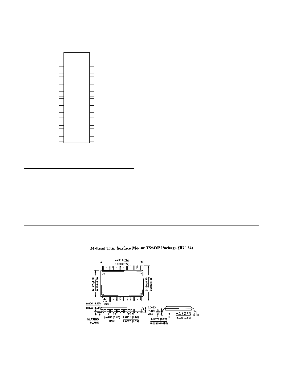
AD5263 PIN CONFIGURATION
AD5263
A2
W1
B3
B4
B1
W2
B2
A1
TSSOP-24
1
2
3
4
24
23
22
21
A3
A4
5
20
V
SS
GND
DIS
SDO/O1
W3
NC/O2
W4
V
DD
6
7
8
9
19
18
17
16
V
LOGIC
SHDN
10
15
SDI/SDA
RESB/AD1
11
14
CLK/SCL
CS
/AD0
12
13
TABLE III: AD5263 PIN Descriptions
Pin Name
Description
1
B1
Resistor terminal B1
2
A1
Resistor terminal A1 (ADDR=00)
3
W1
Wiper terminal W1
4
B3
Resistor terminal B3
5
A3
Resistor terminal A3
6
W3
Wiper terminal W3 (ADDR=10)
7 V
DD
Positive power supply, specified for
+5V to +15V operation
8 GND Ground
9
DIS
Digital Interface Select (SPI/I
2
C
Select); SPI when DIS='0', I
2
C when
DIS='1'
10 V
LOGIC
Logic Supply Voltage, needs to be
same voltage as the digital logic
controlling the AD5263.
11
SDI/SDA
SDI = 3-wire Serial Data Input/ SDA =
2-wire Serial Data Input/Output
12
CLK/SCL
Serial Clock Input
13
CS/AD0
Chip Select / I
2
C Compatabile Device
Address Bit 0
14 RESB/AD1
RESETB/I
2
C Compatabile Device
Address Bit 1
15
SHDN
Shutdown -- Ties wiper to terminal A,
opens terminal B
16
SDO/O1
Serial Data Output, Open Drain
transistor requires pull-up
resistor/Digital Output O1, can be used
to drive external logic
17
NC/O2
No Connection/Digital Output O2, can
be used to drive external logic
18 V
SS
Negative power supply, specified for
operation from 0 to -5V.
19
W4
Wiper terminal W4 (ADDR=11)
20
A4
Resistor terminal A4
21
B4
Resistor terminal B4
22
W2
Wiper terminal W2 (ADDR=01)
23
A2
Resistor terminal A2
24
B2
Resistor terminal B2
OUTLINE DIMENSIONS
Dimensions shown in inches and (mm)
Document Outline