Äîêóìåíòàöèÿ è îïèñàíèÿ www.docs.chipfind.ru
Information furnished by Analog Devices is be lieved to be accurate and
reliable. However, no responsibility is assumed by Analog Devices for its
use, nor for any infringements of patents or other rights of third parties
that may result from its use. No license is granted by implication or other-
wise under any patent or patent rights of Analog Devices. Trademarks and
registered trademarks are the property of their respective companies.
One Technology Way, P.O. Box 9106, Norwood, MA 02062-9106, U.S.A.
Tel: 781/329-4700
www.analog.com
Fax: 781/326-8703 © Analog Devices, Inc., 2002. All rights reserved.
AD5273
64-Position OTP Digital Potentiometer
GENERAL DESCRIPTION
The AD5273 is a 64-position, One-Time-Programmable (OTP)
digital potentiometer
4
that employs fuse link technology to achieve
the permanent program setting. This device performs the same
electronic adjustment function as most mechanical trimmers and
variable resistors. It allows unlimited adjustments before perma-
nently setting the resistance values. The AD5273 is programmed
using a 2-wire, I
2
C compatible digital control. During the write
mode, a fuse blow command is executed after the fi nal value
is determined, therefore freezing the wiper position at a given
setting (analogous to placing epoxy on a mechanical trimmer).
When this permanent setting is achieved, the value will not change
regardless of the supply variations or environmental stresses under
normal operating conditions. To verify the success of permanent
programming, Analog Devices patterned the OTP validation such
that the fuse status can be discerned from two validation bits in
the read mode.
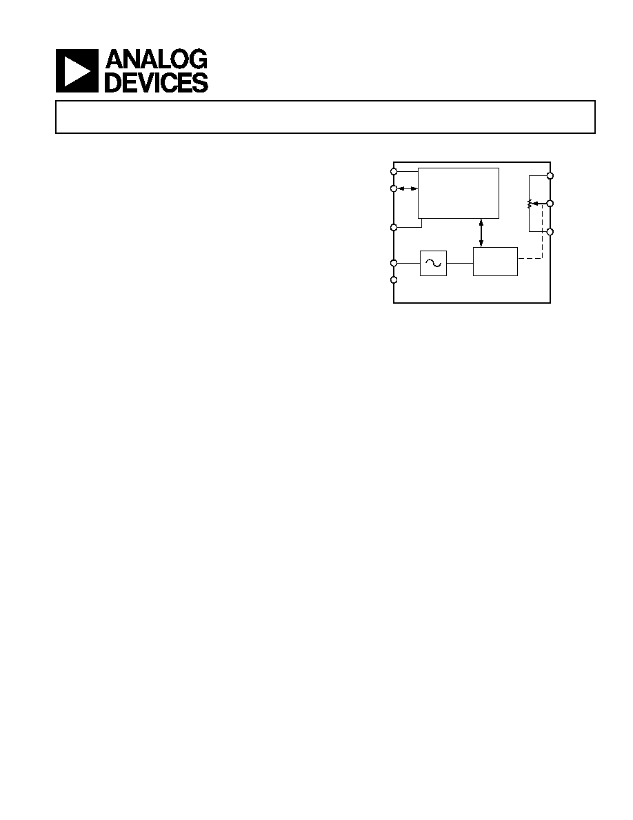
FUNCTIONAL BLOCK DIAGRAM
GND
I
2
C INTERFACE
AND
CONTROL LOGIC
A
W
B
WIPER
REGISTER
FUSE
LINK
V
DD
A0
SDA
SCL
AD5273
In addition, for applications that program AD5273 at the factory,
Analog Devices offers device programming software
2
running in
Windows
®
NT, 2000, and XP operating systems. This software
application effectively replaces any external I
2
C controllers, which
in turn enhances users' systems time-to-market.
AD5273 is available in 1 k , 10 k , 50 k , and 100 k in
compact SOT23 8-lead standard package and operates from
40°C to +105°C.
Besides its unique OTP feature, the AD5273 lends itself well to
general digital potentiometer applications due to its effective
resolution, array resistance options, small footprint, and low cost.
An AD5273 evaluation kit and software are available. The kit includes
the connector and cable that can be converted for further factory
programming applications.
For applications that require dynamic adjustment of resistance
settings with nonvolatile EEMEM, users should refer to AD523x
and AD525x families of nonvolatile memory digital potentiometers.
NOTES
1
One-Time-Programmable--Unlimited adjustments before permanent setting.
2
ADI cannot guarantee the software to be 100% compatible in all systems due to
the wide variations in computer confi gurations.
3
Applies to 1 k parts only.
4
The terms digital potentiometer, VR, and RDAC are used interchangeably.
FEATURES
64 Positions
OTP (One-Time-Programmable)
1
Set-and-Forget
Resistance Setting
1 k , 10 k , 50 k , 100 k End-to-End Terminal Resistance
Compact Standard SOT23-8 Package
Ultralow Power: I
DD
= 5 A Max
Fast Settling Time: t
S
= 5 s Typ in Power-Up
I
2
C Compatible Digital Interface
Computer Software
2
Replaces C in Factory Programming
Applications
Wide Temperature Range: 40 C to +105 C
5 V Programming Voltage
Low Operating Voltage, 2.7 V to 5.5 V
OTP Validation Check Function
APPLICATIONS
Systems Calibrations
Electronics Level Settings
Mechanical Trimmers
®
Replacement in New Designs
Automotive Electronics Adjustments
Transducer Circuits Adjustments
Programmable Filters up to 6 MHz BW
3
REV. 0

2
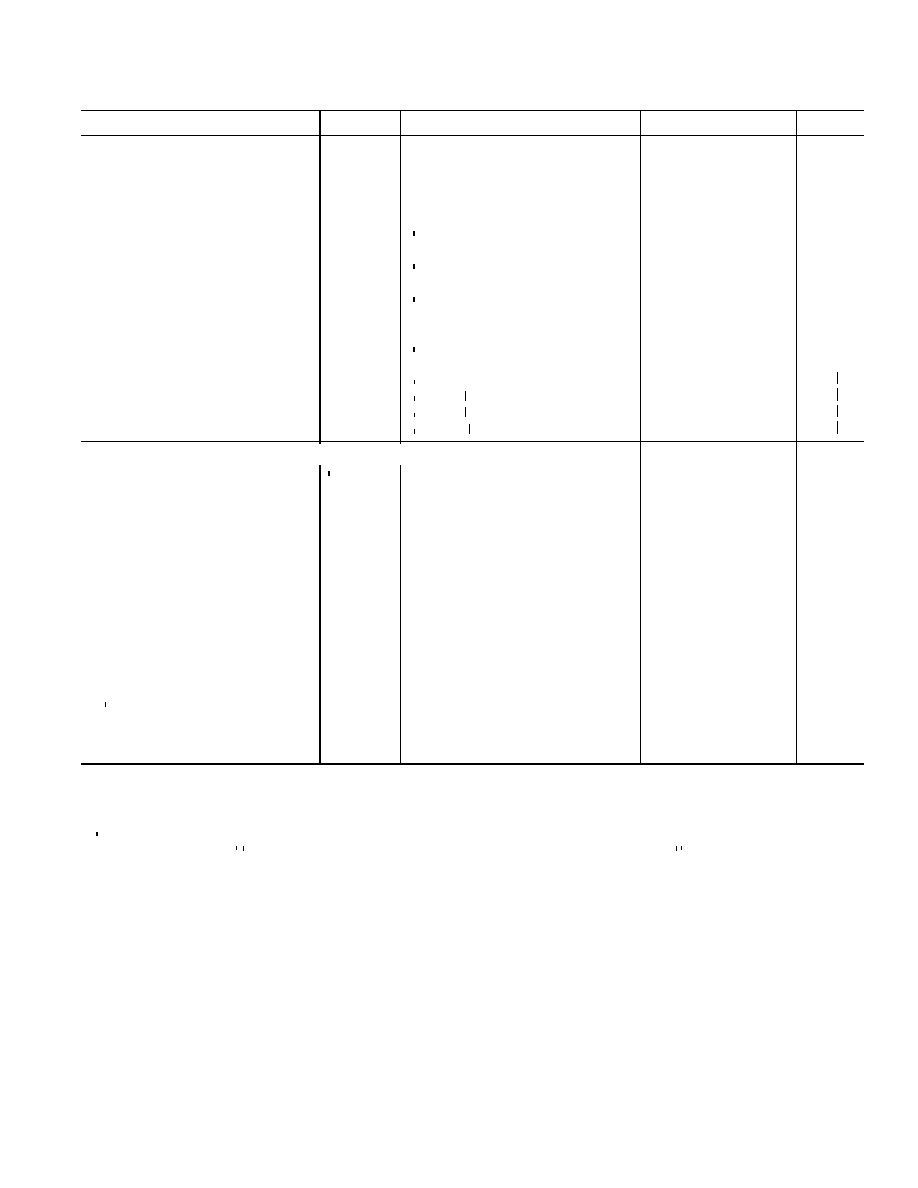
AD5273SPECIFICATIONS
ELECTRICAL CHARACTERISTICS 1 k , 10 k , 50 k , 100 k VERSIONS
(V
DD
= 2.7 V to 5.5 V, V
A
< V
DD
, V
B
= 0 V, 40°C < T
A
< +105°C, unless otherwise noted.)
Parameter Symbol
Conditions
Min
Typ
1
Max Unit
DC CHARACTERISTICS
RHEOSTAT MODE
Resolution
N
6 Bits
Resistor Differential NL
2
R-DNL
(10 k , 50 k , 100 k ) R
WB
, V
A
= NC
0.5
+0.05
+0.5
LSB
(1 k )
R
WB
, V
A
= NC
1
+0.25
+1
LSB
Resistor Nonlinearity
2
R-INL
LSB
(10 k , 50 k , 100 k ) R
WB
, V
A
= NC
0.5
+0.10
+0.5
LSB
(1 k )
R
WB
, V
A
= NC
5
+2
+5
LSB
Nominal Resistance Tolerance
3
R
AB
T
A
= 25°C
(10 k , 50 k , 100 k )
30
+30
%
Nominal Resistance (1 k ) R
AB
0.8 1.2 1.6 k
Resistance Temperature Coeffi cient R
AB
/ T V
AB
= V
DD
, Wiper = No Connect
300
ppm/°C
Wiper Resistance
R
W
I
W
= V
DD
/R, V
DD
= 3 V or 5 V
60
100
DC CHARACTERISTICS
POTENTIOMETER DIVIDER MODE
Differential Nonlinearity
4
DNL
0.5
+0.1
+0.5 LSB
Integral Nonlinearity
4
INL
0.5
+0.5
LSB
Voltage Divider
Temperature Coeffi cient
V
W
/ T Code
=
20
H
10
ppm/°C
Full-Scale Error
V
WFSE
Code = 3F
H
1
0
LSB
Zero-Scale Error
V
WZSE
6
0
LSB
(10 k , 50 k , 100 k ) Code
=
00
H
0 1 LSB
(1 k )
Code
=
00
H
0 5 LSB
RESISTOR TERMINALS
Voltage Range
5
V
A,B,W
0 V
DD
V
Capacitance
6
A, B
C
A,B
f = 5 MHz, Measured to GND,
Code = 20
H
25 pF
Capacitance
6
W C
W
f = 1 MHz, Measured to GND,
Code = 20
H
55 pF
Common Mode Leakage
I
CM
V
A
= V
B
= V
W
1
nA
DIGITAL INPUTS AND OUTPUTS
Input Logic High
V
IH
2.4
V
Input Logic Low
V
IL
0.8 V
Input Logic High
V
IH
V
LOGIC
= 3 V
2.1
V
Input Logic Low
V
IL
V
LOGIC
=
3
V
0.6
V
Output Logic High (SDO)
V
IH
4.9
V
Output Logic Low (SDO)
V
IL
0.4 V
Input Logic Current
I
IL
V
IN
= 0 V or 5 V
0.01
1
µA
Input Capacitance
6
C
IL
5
pF
POWER SUPPLIES
Power Supply Range
V
DD
2.7
5.5 V
OTP Power Supply
7
V
DD_OTP
T
A
= 25°C
5
6
V
Supply Current
I
DD
V
IH
= 5 V or V
IL
= 0 V
0.1
5
µA
OTP Supply Current
8
I
DD_OTP
T
A
= 25°C
100
mA
Power Dissipation
9
P
DISS
V
IH
= 5 V or V
IL
= 0 V, V
DD
= 5 V
0.2 0.3 mW
Power Supply Sensitivity
PSSR
0.015
+0.015
%/%
REV. 0
AD5273
3
Parameter
Symbol
Conditions
Min
Typ
Max
Unit
DYNAMIC CHARACTERISTICS
6, 10, 11
Bandwidth 3 dB
BW_1 k
R
AB
= 1 k, Code = 20
H
6000
kHz
BW_10 k
R
AB
= 10 k, Code = 20
H
600
kHz
BW_50 k R
AB
= 50 k, Code = 20
H
110
kHz
BW_100 k R
AB
= 100 k, Code = 20
H
60
kHz
Total Harmonic Distortion
THD
W
V
A
V
V = 1 V rms, R
AB
= 1 k,
V
B
= 0 V, f = 1 kHz
0.014
%
Adjustment Settling Time
t
S1
V
A
V
V = 5 V ± 1 LSB Error Band, V
B
= 0,
Measured at V
W
5
µs
OTP Settling Time
12
t
S_OTP
V
A
V
V = 5 V ± 1 LSB Error Band, V
B
= 0,
Measured at V
W
400
ms
Power-Up Settling Time
Post Fuses Blown
t
S2
V
A
V
V = 5 V ± 1 LSB Error Band, V
B
= 0,
Measured at V
W
5
µs
Resistor Noise Voltage
e
N_WB
R
AB
R
R = 1 k, f = 1 kHz, Code = 20
H
3
nV/
Hz
R
AB
R
R = 20 k
= 20 k
= 20 k , f = 1 kHz, Code = 20
H
13
nV/
Hz
R
AB
R
R = 50 k
= 50 k
= 50 k , f = 1 kHz, Code = 20
H
20
nV/Hz
R
AB
R
R = 100 k
= 100 k
= 100 k , f = 1 kHz, Code = 20
H
28
nV/Hz
INTERFACE TIMING CHARACTERISTICS (applies to all parts
INTERFACE TIMING CHARACTERISTICS (applies to all parts
6, 11, 13
)
SCL Clock Frequency
f
SCL
f
f
SCL
SCL
400
kHz
t
BUF
Bus Free Time between
STOP and START
t
1
1.3
µs
t
HD;STA
Hold Time
(repeated START)
t
2
After this period, the fi rst clock
pulse is generated.
0.6
µs
t
LOW
Low Period of SCL Clock
t
3
1.3
µs
t
HIGH
High Period of SCL Clock
t
4
0.6
50
µs
t
SU;STA
Setup Time for START
Condition
t
5
0.6
µs
t
HD;DAT
Data Hold Time
t
6
0.9
µs
t
SU;DAT
Data Setup Time
t
7
0.1
µs
t
F
Fall Time of Both SDA and
SCL Signals
t
8
0.3
µs
t
R
Rise Time of Both SDA and
R
R
SCL Signals
t
9
0.3
µs
t
SU;STO
Setup Time for STOP
Condition
t
10
0.6
µs
NOTES
1
Typicals represent average readings at 25°C, V
DD
= 5 V, V
SS
= 0 V.
2
Resistor position nonlinearity error R-INL is the deviation from an ideal value measured between the maximum resistance and the minimum resistance wiper positions.
R-DNL measures the relative step change from ideal between successive tap positions. Parts are guaranteed monotonic.
3
V
AB
V
V = V
DD
, Wiper (V
W
) = No Connect.
4
INL and DNL are measured at V
W
INL and DNL are measured at V
INL and DNL are measured at V with the RDAC confi gured as a potentiometer divider similar to a voltage output D/A converter. V
W
W
A
with the RDAC confi gured as a potentiometer divider similar to a voltage output D/A converter. V
with the RDAC confi gured as a potentiometer divider similar to a voltage output D/A converter. V = V
A
A
DD
and V
B
= 0 V. DNL specifi cation
limits of ±1 LSB maximum are guaranteed monotonic operating conditions.
5
Resistor terminals A, B, W have no limitations on polarity with respect to each other.
6
Guaranteed by design and not subject to production test.
7
Different from operating power supply, power supply for OTP is used one time only.
8
Different from operating current, supply current for OTP lasts approximately 400 ms for one time needed only.
9
P
DISS
is calculated from (I
DD
V
DD
). CMOS logic level inputs result in minimum power dissipation.
10
Bandwidth, noise, and settling time are dependent on the terminal resistance value chosen. The lowest R value results in the fastest settling time and highest bandwidth.
The highest R value results in the minimum overall power consumption.
11
All dynamic characteristics use V
DD
= 5 V.
12
Different from settling time after fuses are blown. The OTP settling time occurs once only.
13
See Figure 1 for location of measured values.
Specifi cations subject to change without notice.
REV. 0

AD5273
4
ORDERING GUIDE
Resistance
Package
Package
Full Container
Model R
AB
(k ) Code Description
Quantities Brand
AD5273BRJ1-REEL7 1
RJ
SOT23-8
3000
DYA
AD5273BRJ10-REEL7 10
RJ
SOT23-8
3000
DYB
AD5273BRJ50-REEL7 50
RJ
SOT23-8
3000
DYC
AD5273BRJ100-REEL7 100
RJ
SOT23-8
3000
DYD
AD5273BRJ1-R2 1
RJ
SOT23-8
250
DYA
AD5273BRJ10-R2 10
RJ
SOT23-8
250
DYB
AD5273BRJ50-R2 50
RJ
SOT23-8
250
DYC
AD5273BRJ100-R2 100
RJ
SOT23-8
250
DYD
AD5273EVAL
*
NA NA
*
NA
*
Users should order samples additionally as the evaluation kit comes with a socket but does not include the parts.
ABSOLUTE MAXIMUM RATINGS
1
(T
A
= 25°C, unless otherwise noted.)
V
DD
to GND . . . . . . . . . . . . . . . . . . . . . . . . . . . . 0.3 V, +6.5 V
V
A
, V
B
, V
W
to GND . . . . . . . . . . . . . . . . . . . . . . . . . . GND, V
DD
AB, AW, BW
Intermittent
2
. . . . . . . . . . . . . . . . . . . . . . . . . . . . . . ±20 mA
Continuous . . . . . . . . . . . . . . . . . . . . . . . . . . . . . . . . . ±2 mA
Digital Input and Output Voltage to GND . . . . . . . . . . 0 V, V
DD
Operating Temperature Range . . . . . . . . . . . . 40°C to +105°C
Maximum Junction Temperature (T
J
MAX
) . . . . . . . . . . . .150°C
Storage Temperature . . . . . . . . . . . . . . . . . . . . 65°C to +150°C
Lead Temperature (Soldering, 10 sec) . . . . . . . . . . . . . . . .300°C
Vapor Phase (60 sec) . . . . . . . . . . . . . . . . . . . . . . . . . . .215°C
Infrared (15 sec) . . . . . . . . . . . . . . . . . . . . . . . . . . . . . .220°C
Thermal Resistance
3
JA
, SOT-23 . . . . . . . . . . . . . . . . 230°C/W
NOTES
1
Stresses above those listed under Absolute Maximum Ratings may cause permanent
damage to the device. This is a stress rating; functional operation of the device at
these or any other conditions above those listed in the operational sections of this
specifi cation is not implied. Exposure to absolute maximum rating conditions for
extended periods may affect device reliability.
2
Maximum terminal current is bounded by the maximum current handling of the
switches, maximum power dissipation of the package, and maximum applied voltage
across any two of the A, B, and W terminals at a given resistance.
3
Package Power Dissipation = (T
J MAX
T
A
)/
JA
CAUTION
ESD (electrostatic discharge) sensitive device. Electrostatic charges as high as 4000 V readily ac cu mu late on
the human body and test equipment and can discharge without detection. Although the AD5273 features
proprietary ESD pro tec tion circuitry, permanent damage may occur on devices subjected to high energy
electrostatic discharges. Therefore, proper ESD pre
cau tions are rec
om mend ed to avoid per
for mance
deg ra da tion or loss of functionality.
REV. 0

AD5273
5
TOP VIEW
(Not to Scale)
8
7
6
5
1
2
3
4
W
V
DD
GND
SCL
A
B
A0
SDA
AD5273
PIN FUNCTION DESCRIPTIONS
Pin No. Mnemonic Description
1 W Wiper Terminal W
2 V
DD
Positive Power Supply. Specifi ed for non-OTP operation from 2.7 V to 5.5 V.
For OTP programming, V
DD
needs to be a minimum of 5 V.
3 GND Common Ground
4 SCL Serial Clock Input. Requires Pull-Up Resistor.
5 SDA Serial Data Input/Output. Requires Pull-Up Resistor.
6 A0 I
2
C Device Address Bit
7 B Resistor Terminal B
8 A Resistor Terminal A
REV. 0
Document Outline
- FEATURES
- APPLICATIONS
- FUNCTIONAL BLOCK DIAGRAM
- GENERAL DESCRIPTION
- SPECIFICATIONS
- ABSOLUTE MAXIMUM RATINGS
- ORDERING GUIDE
- PIN FUNCTION DESCRIPTIONS
- Typical Performance Characteristics
- SDA BITS DEFINITIONS AND DESCRIPTIONS
- THEORY OF OPERATION
- One-Time-Programming (OTP)
- DETERMINING THE VARIABLE RESISTANCE AND VOLTAGE
- Rheostat Operation
- Voltage Output Operation
- ESD PROTECTION
- TERMINAL VOLTAGE OPERATING RANGE
- POWER-UP SEQUENCE
- POWER SUPPLY CONSIDERATIONS
- CONTROLLING THE AD5273
- Software Programming
- Write
- Read
- CONTROLLING TWO DEVICES ON ONE BUS
- APPLICATIONS
- Programmable Voltage Reference
- Programmable Voltage Source with Boosted Output
- Programmable Current Source
- Gain Control Compensation
- Programmable Low-Pass Filter
- Level Shift for Different Voltages Operation
- Resistance Scaling
- Resolution Enhancement
- RDAC CIRCUIT SIMULATION MODEL
- Macro Model Net List for RDAC
- EVALUATION BOARD
- DIGITAL POTENTIOMETER FAMILY SELECTION GUIDE
- OUTLINE DIMENSIONS