AD5290 Compact +30V/±15V 256-Position Digital Potentiometer Preliminary Data Sheet (Rev. PrE)
Compact +30V/±15V 256-Position Digital
Potentiometer
Preliminary Technical Data
AD5290
Rev. PrE
Information furnished by Analog Devices is believed to be accurate and reliable.
However, no responsibility is assumed by Analog Devices for its use, nor for any
infringements of patents or other rights of third parties that may result from its use.
Specifications subject to change without notice. No license is granted by implication
or otherwise under any patent or patent rights of Analog Devices. Trademarks and
registered trademarks are the property of their respective companies.
One Technology Way, P.O. Box 9106, Norwood, MA 02062-9106, U.S.A.
Tel: 781.329.4700
www.analog.com
Fax: 781.326.8703
© 2005 Analog Devices, Inc. All rights reserved.
FEATURES
256-position
+4.5V to +30V Single Supply Operation
±4.5V to ±15V Dual Supply Operation
End-to-end resistance 10 k, 50 k, 100 k
Low temperature coefficient 35 ppm/°C
Power-on preset to midscale
SPI compatible interface
Automotive temperature range 40°C
to +125°C
Compact MSOP-10 (3 mm × 4.9 mm) package
i
CMOSTM
Process Technology
APPLICATIONS
Programmable Gain and Offset
Programmable Power Supply
Industrial Actuator Control
LED Array Driver
Audio Volume Control
General Purpose DAC Replacement
Mechanical Potentiometer Replacement
GENERAL OVERVIEW
The AD5290 is a low cost, compact 2.9 mm × 3 mm
+30V/±15V, 256-position digital potentiometer. This device
performs the same electronic adjustment function as
mechanical potentiometers or variable resistors, with enhanced
resolution, solid-state reliability, and superior low temperature
coefficient performance.
The wiper settings are controllable through an SPI compatible
digital interface. The resistance between the wiper and either
end point of the fixed resistor varies linearly with respect to the
digital code transferred into the RDAC latch.
The AD5290 is available in 10k, 50k, and 100k in compact
MSOP-10 package. AD5290 can be operated from a single
supply +30 V or dual supply ±15 V. All parts are guaranteed to
operate over the automotive temperature range of -40°C to
+125°C.
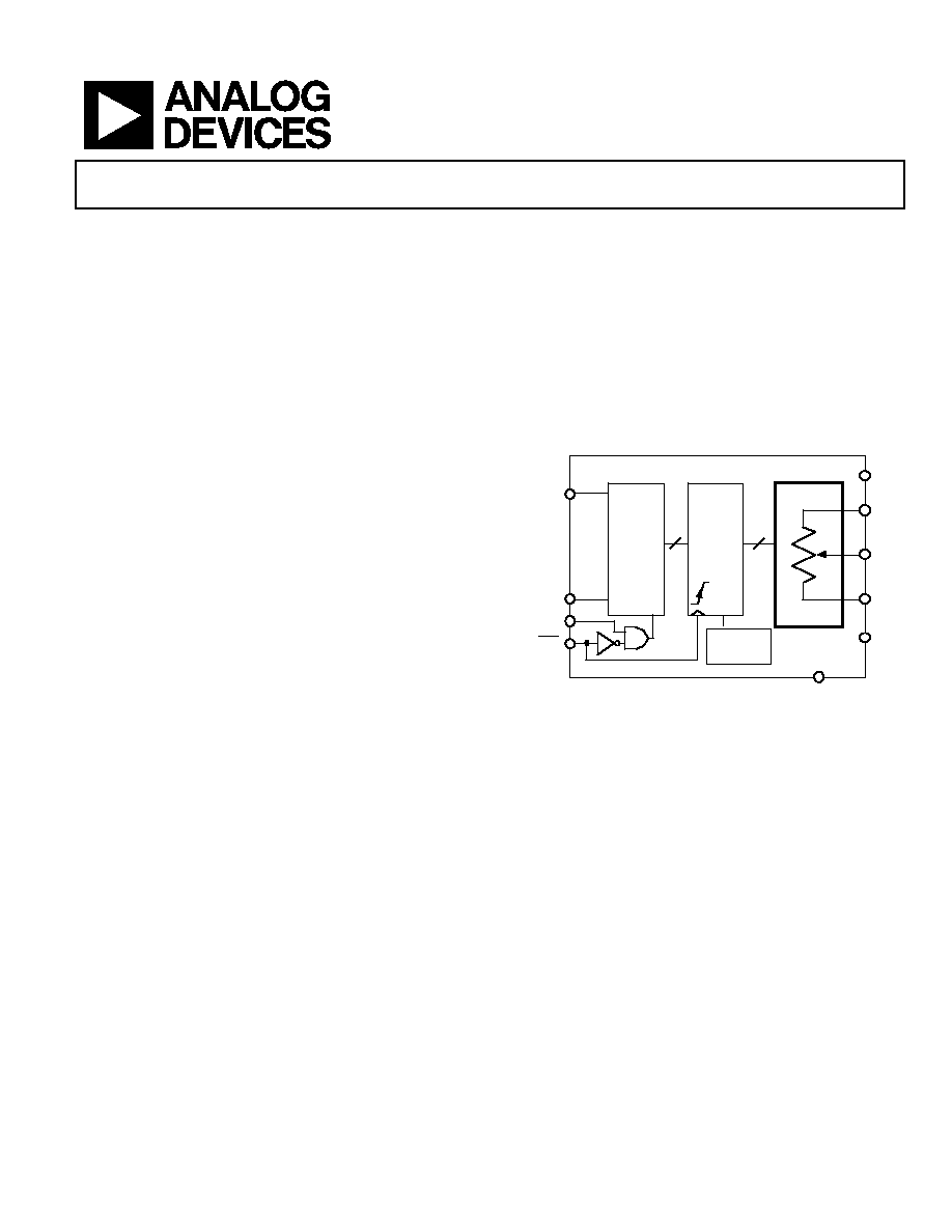
FUNCTIONAL BLOCK DIAGRAM
AD5290
A
W
B
SDO
SDI
CS
DG ND
CLK
Q
D
CK
RS
8-Bit
SERIAL
REG
8-Bit
LATCH
8
8
V
SS
V
DD
POR
AD5290
A
W
B
SDO
SDI
CS
DG ND
CLK
Q
D
CK
RS
8-Bit
SERIAL
REG
8-Bit
LATCH
8
8
V
SS
V
DD
POR
Figure 1.
Note:
The terms digital potentiometer and RDAC are used interchangeably.
i
CMOSTM
Process Technology
For analog systems designers within industrial/instrumentation equipment OEMs who need high performance ICs at higher-voltage levels, iCMOS is a
technology platform that enables the development of analog ICs capable of 30V and operating at +/-15V supplies while allowing dramatic reductions in
power consumption and package size, and increased AC and DC performance.

Preliminary Technical Data
AD5290
Rev. Pr E | Page 2 of 11
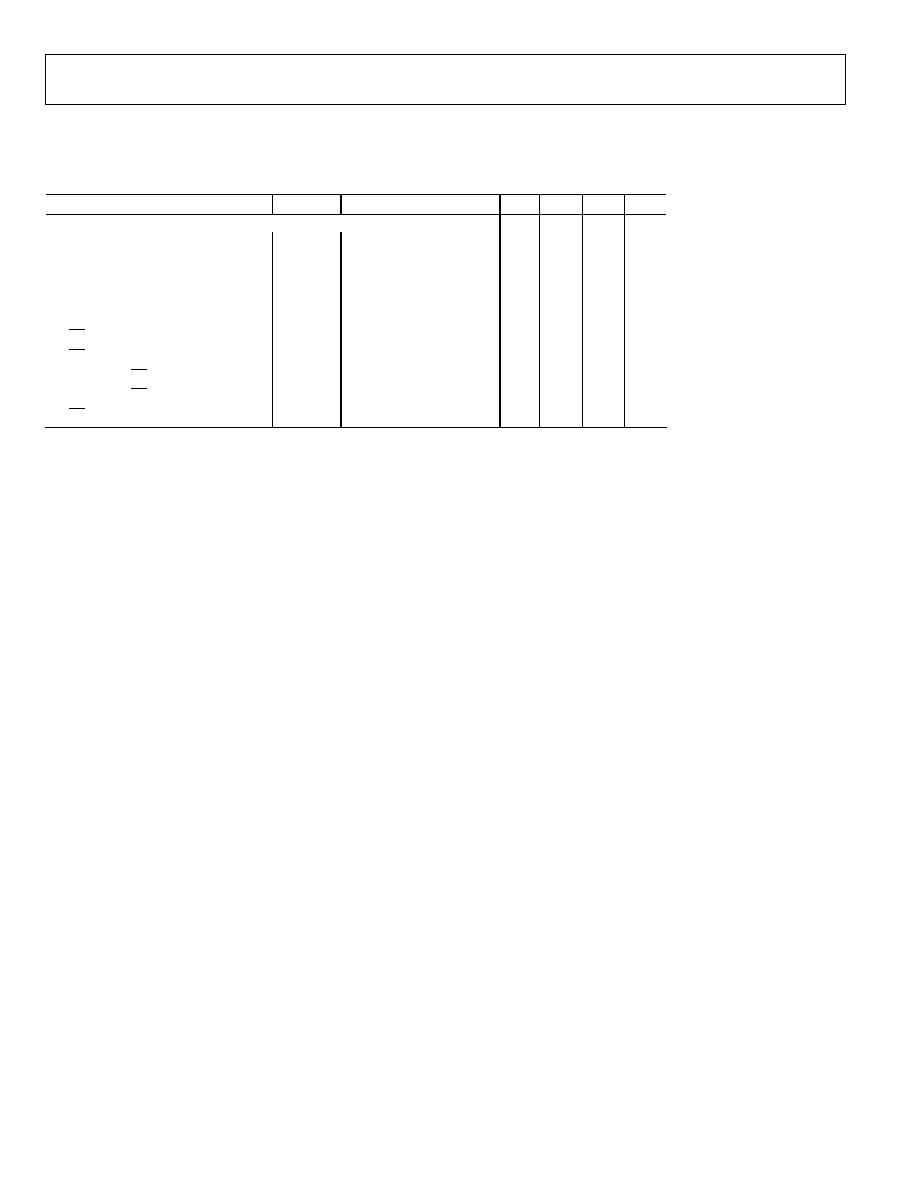
ELECTRICAL CHARACTERISTICS--10 k, 50 k, 100 k VERSIONS
(V
DD
/V
SS
= ±15V±10% or ±5V±10%, V
A
= +V
DD
, V
B
= V
SS
/0V, -40°C < T
A
< +125°C unless otherwise noted)
Table 1.
Parameter Symbol
Conditions
Min
Typ
1
Max
Unit
DC CHARACTERISTICS--RHEOSTAT MODE
Resistor Differential Nonlinearity
2
R-DNL
R
WB
, V
A
= no connect
1
±0.1
+1
LSB
Resistor Integral Nonlinearity
2
R-INL
R
WB
, V
A
= no connect
2
±0.25
+2
LSB
Nominal Resistor Tolerance
3
R
AB
T
A
= 25°C
30
+30
%
Resistance Temperature Coefficient
(R
AB
/R
AB
)/T*10
6
V
AB
= V
DD
,
Wiper = no connect
35
ppm/°C
Wiper
Resistance
R
W
V
DD
= ±15 V
60
150
V
DD
= ±4.5 V
240
450
DC CHARACTERISTICS--POTENTIOMETER DIVIDER MODE
Resolution
N
8
Bits
Differential
Nonlinearity
4
DNL
1
±0.1
+1
LSB
Integral
Nonlinearity
4
INL
1
±0.3
+1
LSB
Voltage Divider Temperature Coefficient
(V
W
/V
W
)/T*10
6
Code = 0x80
5
ppm/°C
Full-Scale
Error
V
WFSE
Code = 0xFF
3
1
0
LSB
Zero-Scale
Error
V
WZSE
Code = 0x00
0
1
3
LSB
RESISTOR TERMINALS
Voltage
Range
5
V
A,B,W
V
SS
V
DD
V
Capacitance
6
A, B
C
A,B
f = 1 MHz, measured to
GND, Code = 0x80
45
pF
Capacitance
6
W
C
W
f = 1 MHz, measured to
GND, Code = 0x80
60
pF
Common-Mode
Leakage
I
CM
V
A
= V
B
= V
W
1
nA
DIGITAL INPUTS AND OUTPUTS
Input Logic High
V
IH
V
DD
= +5V or +15V
2.4
V
Input Logic Low
V
IL
V
DD
= +5V or +15V
0.8
V
Output Logic High
V
OH
R
L
= 2.2 k
to +5 V
4.9
V
Output Logic Low
V
OL
I
OL
= 1.6mA, V
LOGIC
= +5V,
V
DD
= +15V
0.4
V
Input
Current
I
I
V
IN
= 0 V or +15 V
±1
µA
Input
Capacitance
C
I
5
pF
POWER SUPPLIES
Power Supply Range
V
DD
/V
SS
Dual Supply Range
±4.5
±16.5
V
Power Supply Range
V
DD
Single Supply Range, V
SS
=
0 V
+4.5
+30 V
Supply
Current6
I
DD
V
IH
= 5 V or V
IL
= 0 V, V
DD
=
+5 V
0.1
10
µA
Supply
Current
I
DD
V
IH
= 5 V or V
IL
= 0 V, V
DD
=
+15 V
0.75
2 mA
Supply
Current
I
SS
V
IH
= 5 V or V
IL
= 0 V, V
SS
= -
5 V or 15 V
0.02
0.1
mA
Power
Dissipation
7
P
DISS
V
IH
= 5 V or V
IL
= 0 V, V
DD
=
+15 V, V
SS
= -15 V
11
30
mW
Power Supply Sensitivity
PSS
V
DD
= +15V ±10%, or
V
SS
= -15V ±10%, Code =
Midscale
±0.01 ±0.02
%/%
DYNAMIC CHARACTERISTICS
6, 8
Bandwidth
3dB
BW
R
AB
= 10 k/50 k/100 k,
Code = 0x80
525/125/60
kHz

Preliminary Technical Data
AD5290
Rev. Pr E | Page 3 of 11
Total
Harmonic
Distortion
THD
W
V
A
=1 V rms, V
B
= 0 V,
f = 1 kHz, R
AB
= 10 k
0.005 %
V
W
Settling Time (10 k/50 k/100 k)
t
S
V
A
= 5 V, V
B
= 0 V,
±1 LSB error band
4
µs
Resistor Noise Voltage Density
e
N_WB
R
WB
= 25 k
14
nV/Hz
Preliminary Technical Data
AD5290
Rev. Pr E | Page 4 of 11
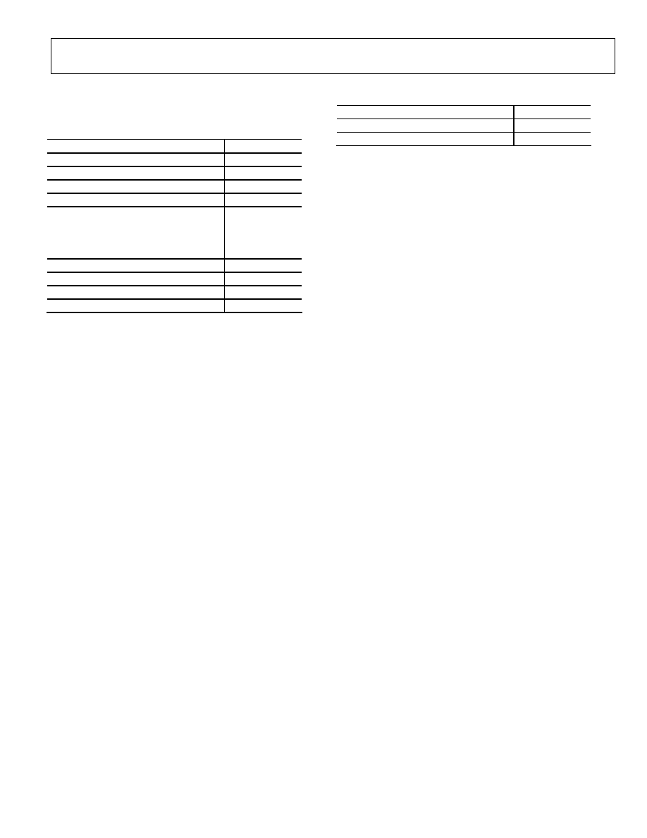
TIMING CHARACTERISTICS-- 10 k, 50 k, 100 k VERSIONS
(V
DD
/V
SS
= ±15V±10% or ±5V±10%, V
A
= +V
DD
, V
B
= 0V, -40°C < T
A
< +125°C unless otherwise noted.)
Table 2.
Parameter Symbol
Conditions
Min
Typ
1
Max Unit
SPI INTERFACE TIMING CHARACTERISTICS
6, 8,9
(Specifications Apply to All Parts)
Clock
Frequency
f
CLK
4 MHz
Input Clock Pulsewidth
t
CH
, t
CL
Clock level high or low
120
ns
Data Setup Time
t
DS
30
ns
Data Hold Time
t
DH
20
ns
CLK to SDO Propagation Delay
t
PD
R
PU
= 1K
, C
L
< 20pF
10
100 ns
CS Setup Time
t
CSS
120
ns
CS High Pulsewidth
t
CSW
150
ns
CLK Fall to CS Fall Hold Time
t
CSH0
TBD
ns
CLK Fall to CS Rise Hold Time
t
CSH1
120
ns
CS Rise to Clock Rise Setup
t
CS1
120
ns
NOTES
1.
Typical specifications represent average readings at +25°C and V
DD
/V
SS
= ±15 V.
2.
Resistor position nonlinearity error R-INL is the deviation from an ideal value measured between the maximum resistance and the minimum resistance wiper
positions. R-DNL measures the relative step change from ideal between successive tap positions. Parts are guaranteed monotonic.
3.
V
AB
= V
DD
, Wiper (V
W
) = no connect.
4.
INL and DNL are measured at V
W
with the RDAC configured as a potentiometer divider similar to a voltage output D/A converter. V
A
=V
DD
and V
B
=0 V.
5.
Resistor terminals A, B, W have no limitations on polarity with respect to each other.
6.
Guaranteed by design and not subject to production test.
7.
P
DISS
is calculated from (I
DD
× V
DD
+ I
SS
× V
SS
) CMOS logic level inputs result in minimum power dissipation.
8.
All dynamic characteristics use V
DD
/ V
SS
= ±15 V.
9.
See timing diagram for location of measured values. All input control voltages are specified with t
R
= t
F
= 2 ns (10% to 90% of 3 V) and timed from a voltage level
of 1.5 V.
Preliminary Technical Data
AD5290
Rev. Pr E | Page 5 of 11
ABSOLUTE MAXIMUM RATINGS
1
(T
A
= +25°C, unless otherwise noted.)
Table 3.
Parameter Value
V
DD
to VSS
0.3 V to +35 V
V
DD
to GND
0.3 V to +35 V
V
SS
to GND
+0.3 V to 16.5 V
V
A
, V
B
, V
W
to GND
V
SS
, V
DD
Maximum Current
I
WB
, I
WA
Pulsed
I
WB
Continuous (R
WB
1
k, A open)
1
I
WA
Continuous (R
WA
1 k, B open)
1
±20 mA
±5 mA
±5 mA
Digital Inputs Voltage to GND
V
DD
+ 0.3 V
Digital Output Voltage to GND
0 V, +7 V
Operating Temperature Range
40°C to +125°C
Maximum Junction Temperature (T
JMAX
) 150°C
Storage Temperature
65°C to +150°C
Lead Temperature (Soldering, 10 30 sec)
245°C
Thermal Resistance
2
JA
: MSOP-10
230°C/W
NOTES
1
Maximum terminal current is bounded by the maximum current handling
of the switches, maximum power dissipation of the package, and maximum
applied voltage across any two of the A, B, and W terminals at a given
resistance.
2
Package power dissipation = (T
JMAX
T
A
)/
JA
.
Stresses above those listed under Absolute Maximum Ratings
may cause permanent damage to the device. This is a stress
rating only and functional operation of the device at these or
any other conditions above those indicated in the operational
section of this specification is not implied. Exposure to
absolute maximum rating conditions for extended periods
may affect device reliability.