 | ÐлекÑÑоннÑй компоненÑ: AD53040 | СкаÑаÑÑ:  PDF PDF  ZIP ZIP |
Äîêóìåíòàöèÿ è îïèñàíèÿ www.docs.chipfind.ru
REV. B
Information furnished by Analog Devices is believed to be accurate and
reliable. However, no responsibility is assumed by Analog Devices for its
use, nor for any infringements of patents or other rights of third parties
which may result from its use. No license is granted by implication or
otherwise under any patent or patent rights of Analog Devices.
a
AD53040
One Technology Way, P.O. Box 9106, Norwood, MA 02062-9106, U.S.A.
Tel: 781/329-4700
World Wide Web Site: http://www.analog.com
Fax: 781/326-8703
© Analog Devices, Inc., 1999
Ultrahigh Speed Pin Driver
with Inhibit Mode
FUNCTIONAL BLOCK DIAGRAM
AD53040
V
LDCPL
TV
CC
THERM
GND
50
DRIVER
V
OUT
V
H
DATA
DATA
INH
INH
V
L
GND
GND
GND
GND
1.0 A/K
V
HDCPL
39nF
39nF
V
CC
V
EE
V
CC
V
EE
FEATURES
500 MHz Driver Operation
Driver Inhibit Function
100 ps Edge Matching
Guaranteed Industry Specifications
50 Output Impedance
>1.5 V/ns Slew Rate
Variable Output Voltages for ECL, TTL and CMOS
High Speed Differential Inputs for Maximum Flexibility
Ultrasmall 20-Lead SOP Package with Built-In Heat Sink
APPLICATIONS
Automatic Test Equipment
Semiconductor Test Systems
Board Test Systems
Instrumentation and Characterization Equipment
PRODUCT DESCRIPTION
The AD53040 is a complete high speed pin driver designed for
use in digital or mixed-signal test systems. Combining a high
speed monolithic process with a unique surface mount package,
this product attains superb electrical performance while preserv-
ing optimum packaging densities and long-term reliability in an
ultrasmall 20-lead, SOP package with built-in heat sink.
Featuring unity gain programmable output levels of 3 V to
+8 V, with output swing capability of less than 100 mV to 9 V,
the AD53040 is designed to stimulate ECL, TTL and CMOS
logic families. The 500 MHz data rate capacity and matched
output impedance allows for real-time stimulation of these
digital logic families. To test I/O devices, the pin driver can
be switched into a high impedance state (Inhibit Mode), electri-
cally removing the driver from the path. The pin driver leakage
current inhibit is typically 100 nA and output charge transfer
entering inhibit is typically less than 20 pC.
The AD53040 transition from HI/LO or to inhibit is controlled
through the data and inhibit inputs. The input circuitry uses
high speed differential inputs with a common-mode range of
±
3 V. This allows for direct interface to precision differential
ECL timing or the simplicity of stimulating the pin driver from a
single ended TTL or CMOS logic source. The analog logic HI/LO
inputs are equally easy to interface. Typically requiring 10
µ
A of
bias current, the AD53040 can be directly coupled to the
output of a digital-to-analog converter.
The AD53040 is available in a 20-lead, SOP package with a
built-in heat sink and is specified to operate over the ambient
commercial temperature range of 25
°
C to +85
°
C.
2
REV. B
AD53040SPECIFICATIONS
(All specifications are at T
J
= +85 C 5 C, +V
S
= +12 V 3%, V
S
= 7 V
3% unless otherwise noted. All temperature coefficients are measured at T
J
= +75 C95 C). (A 39 nF capacitor must be connected between
V
CC
and V
HDCPL
and between V
EE
and V
LDCPL
.)
Parameter
Min
Typ
Max
Units
Test Conditions
DIFFERENTIAL INPUT CHARACTERISTICS
Input Swing (Data to
DATA, INH to INH)
ECL
2
Volts
Max (DATA,
DATA) to Min (INH, INH)
Max (INH,
INH) to Min (Data, DATA)
2
Volts
Bias Current
±
10
µ
A
V
IN
= 2 V, 0.0 V
REFERENCE INPUTS
Bias Currents
50
+50
µ
A
V
L
, V
H
= 5 V
OUTPUT CHARACTERISTICS
Logic High Range
2
+8
Volts
DATA = H, V
H
= 2 V to +8 V
V
L
= 3 V (V
H
= 2 V to +6 V)
V
L
= 1 V (V
H
= +6 V to +8 V)
Logic Low Range
3
+5
Volts
DATA = L, V
L
= 3 V to +5 V, V
H
= +6 V
Amplitude (V
H
and V
L
)
0.1
9
Volts
V
L
= 0.05 V, V
H
= +0.05 V and
V
L
= 2 V, V
H
= +7 V
Absolute Accuracy
V
H
Offset
100
+100
mV
DATA = H, V
H
= 2 V to +8 V, V
L
= 3 V
V
H
Gain + Linearity Error
±
0.3
±
5
% of V
H
+ mV
DATA = H, V
H
= 2 V to +8 V, V
L
= 3 V
V
L
Offset
100
+100
mV
DATA = L, V
L
= 3 V to +5 V, V
H
= +6 V
V
L
Gain + Linearity Error
±
0.3
±
5
% of V
L
+ mV
DATA = L, V
L
= 3 V to +5 V, V
H
= +6 V
Offset TC, V
H
or V
L
0.5
mV/
°
C
V
L
, V
H
= 0 V, +5 V and 3 V, 0 V
Output Resistance
45
47
49
DATA = H, V
H
= +3 V, V
L
= 0 V,
I
OUT
= 30 mA
Output Leakage
1.0
+1.0
µ
A
V
OUT
= 3 V to +8 V
Dynamic Current Limit
150
mA
C
BYP
= 39 nF, V
H
= +7 V, V
L
= 2 V
Static Current Limit
±
65
mA
Output to 3 V, V
H
= +8 V, V
L
= 1 V,
DATA = H and Output to +8 V, V
H
= +6 V,
V
L
= 3 V, DATA = L
PSRR, Drive Mode
35
dB
V
S
= V
S
±
3%
DYNAMIC PERFORMANCE, DRIVE
(V
H
and V
L
)
Propagation Delay Time
1.5
ns
Measured at 50%, V
H
= +400 mV,
V
L
= 400 mV
Propagation Delay TC
2
ps/
°
C
Measured at 50%, V
H
= +400 mV,
V
L
= 400 mV
Delay Matching, Edge to Edge
100
ps
Measured at 50%, V
H
= +400 mV,
V
L
= 400 mV
Rise and Fall Time
1 V Swing
0.8
ns
Measured 20%80%, V
L
= 0 V, V
H
= 1 V
3 V Swing
1.7
ns
Measured 10%90%, V
L
= 0 V, V
H
= 3 V
5 V Swing
2.4
ns
Measured 10%90%, V
L
= 0 V, V
H
= 5 V
Rise and Fall Time TC
1 V Swing
±
1
ps/
°
C
Measured 20%80%, V
L
= 0 V, V
H
= 1 V
3 V Swing
±
2
ps/
°
C
Measured 10%90%, V
L
= 0 V, V
H
= 3 V
5 V Swing
±
3
ps/
°
C
Measured 10%90%, V
L
= 0 V, V
H
= 5 V
Overshoot, Undershoot and Preshoot
±
(1% +50 mV)
% of Step + mV
a. V
L
, V
H
= 0.0 V, 1.0 V
b. V
L
, V
H
= 0.0 V, 3.0 V
c. V
L
, V
H
= 0.0 V, 5.0 V
Settling Time
to 15 mV
40
ns
V
L
= 0 V, V
H
= 0.5 V
to 4 mV
8
µ
s
V
L
= 0 V, V
H
= 0.5 V
Delay Change vs. Pulsewidth
50
ps
V
L
= 0 V, V
H
= 2 V,
Pulsewidth = 2.5 ns/7.5 ns, 30 ns/100 ns
3
REV. B
AD53040
CAUTION
ESD (electrostatic discharge) sensitive device. Electrostatic charges as high as 4000 V readily
accumulate on the human body and test equipment and can discharge without detection.
Although the AD53040 features proprietary ESD protection circuitry, permanent damage may
occur on devices subjected to high energy electrostatic discharges. Therefore, proper ESD
precautions are recommended to avoid performance degradation or loss of functionality.
Parameter
Min
Typ
Max
Units
Test Conditions
DYNAMIC PERFORMANCE, DRIVE
(V
H
and V
L
) (Continued)
Minimum Pulsewidth
3 V Swing
1.7
ns
4.0 ns Input, 10%/90% Output,
V
L
= 0 V, V
H
= 3 V
5 V Swing
2.6
ns
6.0 ns Input, 10%/90% Output,
V
L
= 0 V, V
H
= 5 V
Toggle Rate
500
MHz
V
L
= 1.8 V, V
H
= 0.8 V,
V
OUT
> 600 mV p-p
DYNAMIC PERFORMANCE, INHIBIT
Delay Time, Active to Inhibit
2
5
ns
Measured at 50%, V
H
= +2 V,
V
L
= 2 V
Delay Time, Inhibit to Active
2
5
ns
Measured at 50%, V
H
= +2 V,
V
L
= 2 V
I/O Spike
<200
mV, p-p
V
H
= 0 V, V
L
= 0 V
Output Capacitance
5
pF
Driver Inhibited
POWER SUPPLIES
Total Supply Range
19
V
Positive Supply
+12
V
Negative Supply
7
V
Positive Supply Current
75
mA
Negative Supply Current
75
mA
Total Power Dissipation
1.15
1.43
W
Temperature Sensor Gain Factor
1.0
µ
A/K
R
LOAD
= 10 K, V
SOURCE
= +12 V
NOTES
Connecting or shorting the decoupling capacitors to ground will result in the destruction of the device.
Specifications subject to change without notice.
ORDERING GUIDE
Shipment Method,
Package
Quantity Per
Package
Model
Description
Shipping Container Option
AD53040KRP 20-Lead Power SOIC Tube, 38 Pieces
RP-20
ABSOLUTE MAXIMUM RATINGS
1
Power Supply Voltage
+V
S
to GND . . . . . . . . . . . . . . . . . . . . . . . . . . . . . . . +13 V
V
S
to GND . . . . . . . . . . . . . . . . . . . . . . . . . . . . . . . . . 8 V
+V
S
to V
S
. . . . . . . . . . . . . . . . . . . . . . . . . . . . . . . . . +20 V
Inputs
DATA,
DATA, INH, INH . . . . . . . . . . . . . . . . +5 V, 3 V
DATA to
DATA, INH to INH . . . . . . . . . . . . . . . . . .
±
3 V
V
H
, V
L
to GND . . . . . . . . . . . . . . . . . . . . . . . . . +9 V, 4 V
V
H
to V
L
. . . . . . . . . . . . . . . . . . . . . . . . . . . . . . +11 V, 0 V
Outputs
V
OUT
Short Circuit Duration . . . . . . . . . . . . . . . . Indefinite
2
V
OUT
Range in Inhibit Mode
V
HDCPL
. . . . . Do Not Connect Except for Capacitor to V
CC
V
LDCPL
. . . . . Do Not Connect Except for Capacitor to V
EE
THERM . . . . . . . . . . . . . . . . . . . . . . . . . . . . . . +13 V, 0 V
Environmental
Operating Temperature (Junction) . . . . . . . . . . . . . . +175
°
C
Storage Temperature . . . . . . . . . . . . . . . . 65
°
C to +150
°
C
Lead Temperature (Soldering, 10 sec)
3
. . . . . . . . . . +260
°
C
NOTES
1
Stresses above those listed under Absolute Maximum Ratings may cause perma-
nent damage to the device. This is a stress rating only; functional operation of the
device at these or any other conditions above those indicated in the operational
sections of this specification is not implied. Absolute maximum limits apply
individually, not in combination. Exposure to absolute maximum rating conditions
for extended periods may affect device reliability.
2
Output
short circuit protection is guaranteed as long as proper heat sinking is
employed to ensure compliance with the operating temperature limits.
3
To ensure lead coplanarity (
±
0.002 inches) and solderability, handling with bare
hands should be avoided and the device should be stored in environments at 24
°
C
±
5
°
C (75
°
F
±
10
°
F) with relative humidity not to exceed 65%.
WARNING!
ESD SENSITIVE DEVICE
AD53040
4
REV. B
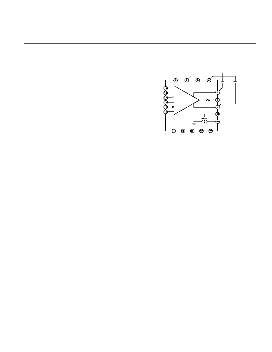
PIN FUNCTION DESCRIPTIONS
Pin
Pin
Name
Number
Pin Functional Description
V
CC
1, 2
Positive Power Supply. Both pins
should be connected to minimize in-
ductance and allow maximum speed of
operation. V
CC
should be decoupled to
GND with a low inductance 0.1
µ
F
capacitor.
V
EE
8, 9
Negative Power Supply. Both pins
should be connected to keep the induc-
tance down and allow maximum speed
of operation. V
EE
should be decoupled
to GND with a low inductance 0.1
µ
F
capacitor.
GND
4, 6, 14,
16, 17
Device Ground. These pins should be
connected to the circuit board's ground
plane at the pins.
V
L
15
Analog Input that sets the voltage level
of a Logic 0 of the driver. Determines
the driver output for
DATA > DATA.
V
H
18
Analog input that sets the voltage level
of a Logic 1 of the driver. Determines
the driver output for DATA >
DATA.
V
OUT
5
The Driver Output. The nominal out-
put impedance is 50
.
V
HDCPL
3
Internal supply decoupling for the
output stage. This pin is connected
to V
CC
through a 39 nF minimum
capacitors.
V
LDCPL
7
Internal supply decoupling for the
output stage. This pin is connected
to V
EE
through a 39 nF minimum
capacitors.
INH,
INH 10, 11
ECL compatible input that control the
high impedance state of the driver.
When INH >
INH, the driver goes into
a high impedance state.
DATA,
13, 12
ECL compatible inputs that determines
DATA
the high and low state of the driver.
Driver output is high for DATA >
DATA.
TV
CC
19
Temperature Sensor Start-Up Pin. This
pin should be connected to V
CC
.
THERM
20
Temperature Sensor Output Pin. A
resistor (10K) should be connected
between THERM and V
CC
. The ap-
proximate die temperature can be de-
termined by measuring the current
through the resistor. The typical scale
factor is 1
µ
A/K.
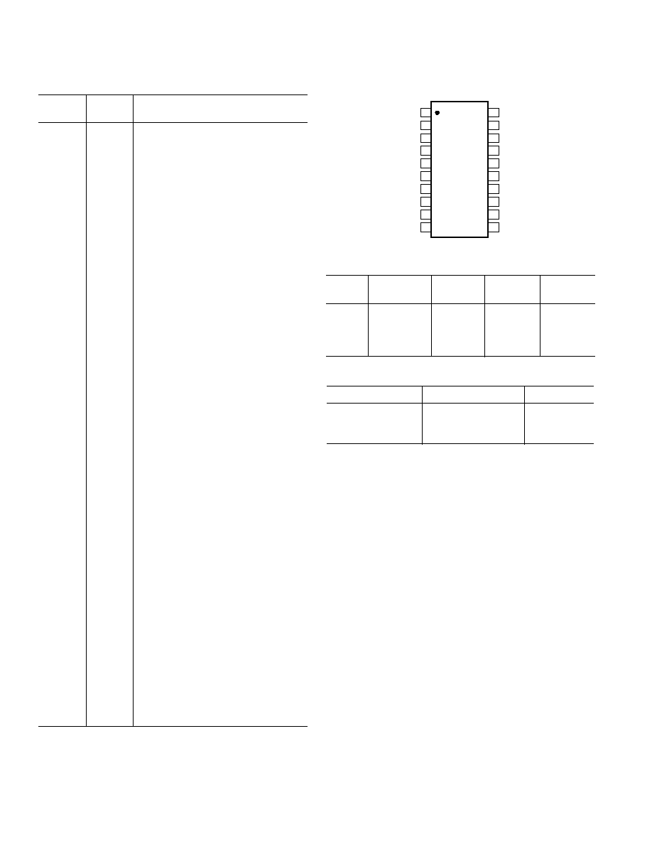
PIN CONFIGURATION
14
13
12
17
16
15
19
18
11
20
10
9
8
1
2
3
4
7
6
5
TOP VIEW
(Not to Scale)
V
CC
GND
V
H
TV
CC
THERM
V
CC
V
HDCPL
GND
AD53040
GND
V
L
GND
V
OUT
GND
V
LDCPL
V
EE
V
EE
INH
INH
DATA
DATA
COPPER
SLUG UP
Table I. Pin Driver Truth Table
Output
DATA
DATA
INH
INH
State
0
1
0
1
V
L
1
0
0
1
V
H
0
1
1
0
Hi-Z
1
0
1
0
Hi-Z
Table II. Package Thermal Characteristics
Air Flow, FM
JC
, C/W
JA
, C/W
0
4
50
50
4
49
400
4
34
AD53040
5
REV. B
APPLICATION INFORMATION
Power Supply Distribution, Bypassing and Sequencing
The AD53040 draws substantial transient currents from its
power supplies when switching between states and careful design
of the power distribution and bypassing is key to obtaining speci-
fied performance. Supplies should be distributed using broad,
low inductance traces or (preferably) planes in a multilayered
board with a dedicated ground-plane layer. All of the device's
power supply pins should be used to minimize the internal in-
ductance presented by the part's bond wires. Each supply must
be bypassed to ground with at least one 0.1
µ
F capacitor; chip-
style capacitors are preferable as they minimize inductance. One
or more 10
µ
F (or greater) Tantalum capacitors per board are
also advisable to provide additional local energy storage.
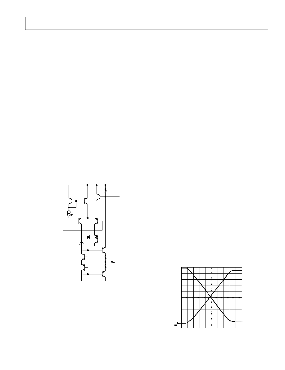
The AD53040's current-limit circuitry also requires external
bypass capacitors. Figure 1 shows a simplified schematic of the
positive current-limit circuit. Excessive collector current in out-
put transistor Q49 creates a voltage drop across the 10
resis-
tor, which turns on PNP transistor Q48. Q48 diverts the rising-
edge slew current, shutting down the current mirror and remov-
ing the output stage's base drive. The V
HDCPL
pin should be
bypassed to the positive supply with a 0.039
µ
F capacitor, while
the V
LDCPL
pin (not shown) requires a similar capacitor to the
negative supply- these capacitors ensure that the AD53040
doesn't current limit during normal output transitions up the its
full 9 V rated step size. Both capacitors must have minimum-
length connections to the AD53040. Here again, chip capacitors
are ideal.
RISING-EDGE SLEW
CONTROL CURRENT
LEVEL-SHIFTED
LOGIC DRIVE
VPOS
V
HDCPL
V
H
OUT
Q50
Q49
VNEG
Q48
10
10%
Figure 1. Simplified Schematic of the AD53040 Output
Stage and Positive Current Limit Circuitry
Several points about the current-limit circuitry should be noted.
First, the limiting currents are not tightly controlled, as they are
functions of both absolute transistor V
BES
and junction tem-
perature; higher dc output current is available at lower junction
temperatures. Second, it is essential to connect the V
HDCPL
capacitor to the positive supply (and the V
LDCPL
capacitor to
the negative supply)--failure to do so causes considerable ther-
mal stress in the current-limiting resistor(s) during normal sup-
ply sequencing and may ultimately cause them to fail, rendering
the part nonfunctional. Finally, the AD53040 may appear to
function normally for small output steps (less than 3 V or so) if
one or both of these capacitors is absent, but it will exhibit
excessive rise or fall times for steps of larger amplitude.
The AD53040 does not require special power-supply sequencing.
However, good design practice dictates that digital and analog
control signals not be applied to the part before the supplies are
stable. Violating this guideline will not normally destroy the
part, but the active inputs can draw considerable current until
the main supplies are applied.
Digital Input Range Restrictions
Total range amongst all digital signals (DATA,
DATA, INH,
and
INH) has to be less than or equal to 2 V to meet specified
timing. The device will function above 2 V with reduced perfor-
mance up to the absolute maximum limit. This performance
degradation might not be noticed in all modes of operation. Of
all the six possible transitions (V
H
v V
L
, V
L
v V
H
, V
H
v INH,
INH
v V
H
, V
L
v INH and INH v V
L
), there may be only one
that would show a degradation, usually in delay time. Taken to
the extreme, the driver may fail to achieve a proper output volt-
age, output impedance or may fail to fully inhibit.
An example of a scenario that would not work for the AD53040
is if the part is driven using 5 V single-ended CMOS. One pin of
each differential input would be tied to a +2.5 V reference level
and the logic voltages would be applied to the other. This would
meet the Absolute Maximum Rating of
±
3 V because the max
differential is
±
2.5 V. It is however possible, for example for
0.0 V to be applied to the INH input and +5 V to be applied to
the DATA input. This 5 V difference far exceeds the 2.0 V
limitation given above. Even using 3 V CMOS or TTL the
difference between logic high and logic low is greater than or
equal to 3 V which will not properly work. The only solution is
to use resistive dividers or equivalent to reduce the voltage levels.
5.12V
550mV
/DIV
380mV
66.25ns
500ps/DIV
71.25ns
Figure 2. 5 V Output Swing