 | ÐлекÑÑоннÑй компоненÑ: AD5307ARU | СкаÑаÑÑ:  PDF PDF  ZIP ZIP |
þÿ
2.5 V to 5.5 V, 400 A, Quad Voltage Output,
8-/10-/12-Bit DACs in 16-Lead TSSOP
AD5307/AD5317/AD5327
Rev. C
Information furnished by Analog Devices is believed to be accurate and reliable. However, no
responsibility is assumed by Analog Devices for its use, nor for any infringements of patents or other
rights of third parties that may result from its use. Specifications subject to change without notice. No
license is granted by implication or otherwise under any patent or patent rights of Analog Devices.
Trademarks and registered trademarks are the property of their respective owners.
One Technology Way, P.O. Box 9106, Norwood, MA 02062-9106, U.S.A.
Tel: 781.329.4700
www.analog.com
Fax: 781.461.3113
©2006 Analog Devices, Inc. All rights reserved.
FEATURES
AD5307: 4 buffered 8-bit DACs in 16-lead TSSOP
A version: ±1 LSB INL; B version: ±0.625 LSB INL
AD5317: 4 buffered 10-bit DACs in 16-lead TSSOP
A version: ±4 LSB INL; B version: ±2.5 LSB INL
AD5327: 4 buffered 12-bit DACs in 16-lead TSSOP
A version: ±16 LSB INL; B version: ±10 LSB INL
Low power operation: 400 A @ 3 V, 500 A @ 5 V
2.5 V to 5.5 V power supply
Guaranteed monotonic by design over all codes
Power down to 90 nA @ 3 V, 300 nA @ 5 V (LDAC pin)
Double-buffered input logic
Buffered/unbuffered reference input options
Output range: 0 V to V
REF
or 0 V to 2 V
REF
Power-on reset to 0 V
Simultaneous update of outputs (LDAC pin)
Asynchronous clear facility (CLR pin)
Low power, SPI®-, QSPITM-, MICROWIRETM-, and DSP-
compatible 3-wire serial interface
SDO daisy-chaining option
On-chip rail-to-rail output buffer amplifiers
Temperature range of -40°C to +105°C
APPLICATIONS
Portable battery-powered instruments
Digital gain and offset adjustment
Programmable voltage and current sources
Programmable attenuators
Industrial process control
GENERAL DESCRIPTION
The AD5307/AD5317/AD5327
1
are quad 8-,10-,12-bit buffered
voltage-output DACs in 16-lead TSSOP that operate from single
2.5 V to 5.5 V supplies and consume 400 A at 3 V. Their on-
chip output amplifiers allow the outputs to swing rail-to-rail with
a slew rate of 0.7 V/s. The AD5307/AD5317/AD5327 utilize
versatile 3-wire serial interfaces that operate at clock rates up to
30 MHz; these parts are compatible with standard SPI, QSPI,
MICROWIRE, and DSP interface standards.
The references for the four DACs are derived from two reference
pins (one per DAC pair). These reference inputs can be configured
as buffered or unbuffered inputs. Each part incorporates a power-
on reset circuit, ensuring that the DAC outputs power up to 0 V
and remain there until a valid write to the device takes place.
There is also an asynchronous active low CLR pin that clears all
DACs to 0 V. The outputs of all DACs can be updated simul-
taneously using the asynchronous LDAC input. Each part
contains a power-down feature that reduces the current
consumption of the device to 300 nA @ 5 V (90 nA @ 3 V). The
parts can also be used in daisy-chaining applications using the
SDO pin.
All three parts are offered in the same pinout, allowing users to
select the amount of resolution appropriate for their application
without redesigning their circuit board.
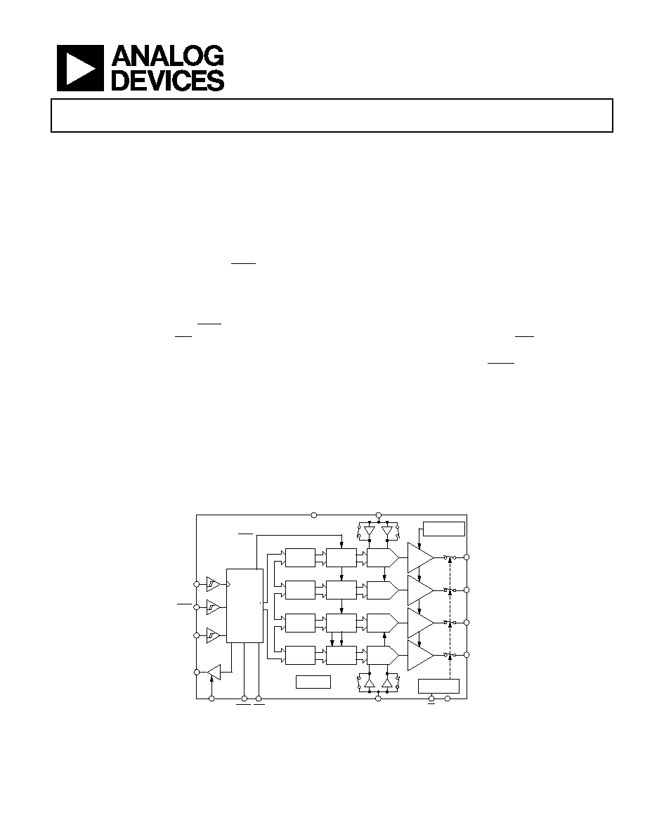
FUNCTIONAL BLOCK DIAGRAM
V
DD
V
REF
AB
V
REF
CD
POWER-ON
RESET
POWER-DOWN
LOGIC
GND
AD5307/AD5317/AD5327
LDAC
PD
LDAC CLR
DCEN
SDO
DIN
SYNC
SCLK
BUFFER
BUFFER
BUFFER
BUFFER
INPUT
REGISTER
DAC
REGISTER
STRING
DAC D
INPUT
REGISTER
DAC
REGISTER
STRING
DAC C
INPUT
REGISTER
DAC
REGISTER
STRING
DAC B
INPUT
REGISTER
DAC
REGISTER
STRING
DAC A
V
OUT
D
V
OUT
C
V
OUT
B
V
OUT
A
GAIN-SELECT
LOGIC
INTERFACE
LOGIC
02067-
001
Figure 1.
1
Protected by U.S. Patent No. 5,969,657; other patents pending.

AD5307/AD5317/AD5327
Rev. C | Page 2 of 28
TABLE OF CONTENTS
Features .............................................................................................. 1
Applications....................................................................................... 1
General Description ......................................................................... 1
Functional Block Diagram .............................................................. 1
Revision History ............................................................................... 2
Specifications..................................................................................... 3
AC Characteristics........................................................................ 5
Timing Characteristics ................................................................ 5
Absolute Maximum Ratings............................................................ 7
ESD Caution.................................................................................. 7
Pin Configuration and Function Descriptions............................. 8
Typical Performance Characteristics ............................................. 9
Terminology .................................................................................... 13
Transfer Function ........................................................................... 14
Functional Description .................................................................. 15
Digital-to-Analog Section ......................................................... 15
Resistor String ............................................................................. 15
DAC Reference Inputs ............................................................... 15
Output Amplifier........................................................................ 16
Power-On Reset .......................................................................... 16
Serial Interface ................................................................................ 17
Input Shift Register .................................................................... 17
Control Bits ................................................................................. 17
Low Power Serial Interface ....................................................... 18
Daisy Chaining ........................................................................... 18
Double-Buffered Interface ........................................................ 18
Load DAC Input (LDAC).......................................................... 18
Power-Down Mode .................................................................... 18
Microprocessor Interfacing....................................................... 19
Applications..................................................................................... 20
Typical Application Circuit....................................................... 20
Driving V
DD
from the Reference Voltage ................................ 20
Bipolar Operation....................................................................... 20
Opto-Isolated Interface for Process-Control Applications... 21
Decoding Multiple AD5307/AD5317/AD5327 Devices....... 21
AD5307/AD5317/AD5327 as Digitally Programmable
Window Detectors ..................................................................... 21
Daisy Chaining ........................................................................... 22
Power Supply Bypassing and Grounding................................ 22
Outline Dimensions ....................................................................... 24
Ordering Guide .......................................................................... 25
REVISION HISTORY
3/06--Rev. B to Rev. C
Changes to Table 3............................................................................ 5
Changes to Ordering Guide .......................................................... 25
10/05--Rev. A to Rev. B
Updated Format..................................................................Universal
Changes to Bipolar Operation Section ........................................ 21
Changes to Ordering Guide .......................................................... 25
8/03--Rev. 0 to Rev. A
Added A Version ................................................................Universal
Changes to Features ..........................................................................1
Changes to Specifications.................................................................2
Changes to Absolute Maximum Ratings........................................6
Changes to Ordering Guide .............................................................6
Changes to TPC 21......................................................................... 12
Added Octals section to Table II .................................................. 20
Updated Outline Dimensions....................................................... 21

AD5307/AD5317/AD5327
Rev. C | Page 3 of 28
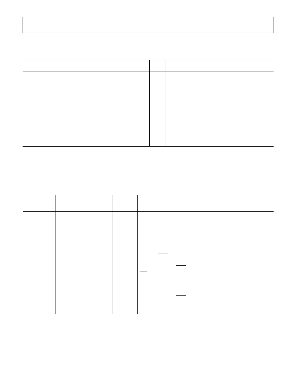
SPECIFICATIONS
V
DD
= 2.5 V to 5.5 V, V
REF
= 2 V, R
L
= 2 k to GND, C
L
= 200 pF to GND. All specifications T
MIN
to T
MAX
, unless otherwise noted.
Table 1.
A
Version
1
B Version
Parameter
2
Min
Typ
Max
Min
Typ
Max
Unit
Conditions/Comments
DC PERFORMANCE
3 , 4
AD5307
Resolution
8
8
Bits
Relative Accuracy
±0.15
±1
±0.15
±0.625
LSB
Differential Nonlinearity
±0.02
±0.25
±0.02
±0.25
LSB
Guaranteed monotonic by design
over all codes
AD5317
Resolution
10
10
Bits
Relative
Accuracy
±0.5 ±4
±0.5 ±2.5 LSB
Differential Nonlinearity
±0.05
±0.5
±0.05
±0.5
LSB
Guaranteed monotonic by design
over all codes
AD5327
Resolution
12
12
Bits
Relative
Accuracy
±2 ±16
±2 ±10
LSB
Differential Nonlinearity
±0.2
±1
±0.2
±1
LSB
Guaranteed monotonic by design
over all codes
Offset Error
±5
±60
±5
±60
mV
V
DD
= 4.5 V, gain = 2; see Figure 29
and Figure 30
Gain Error
±0.3
±1.25
±0.3
±1.25
% FSR
V
DD
= 4.5 V, gain = 2; see Figure 29
and Figure 30
Lower Dead Band
5
10 60
10 60 mV See
Figure 29, lower dead band
exists only if offset error is negative
Upper Dead Band
10 60
10 60 mV See
Figure 30, upper dead band
exists only if V
REF
= V
DD
and offset
plus gain error is positive
Offset Error Drift
6
-12
-12
ppm
of
FSR/°C
Gain Error Drift
-5
-5
ppm
of
FSR/°C
DC Power Supply Rejection Ratio
-60
-60
dB
V
DD
= ±10%
DC Crosstalk
200
200
mV
R
L
= 2 k to GND or V
DD
DAC REFERENCE INPUTS
V
REF
Input Range
1
V
DD
1 V
DD
V Buffered
reference
mode
0.25
V
DD
0.25
V
DD
V Unbuffered
reference
mode
V
REF
Input Impedance (R
DAC
)
>10
>10
M
Buffered reference mode and
power-down mode
74
90
74
90
k
Unbuffered reference mode,
0 V to V
REF
output range
37
45
37
45
k
Unbuffered reference mode,
0 V to 2 V
REF
output range
Reference Feedthrough
-90
-90
dB
Frequency = 10 kHz
Channel-to-Channel Isolation
-75
-75
dB
Frequency = 10 kHz
OUTPUT CHARACTERISTICS
Minimum Output Voltage
7
0.001
0.001
V
A
measure
of
the
minimum
drive
capability of the output amplifier
Maximum Output Voltage
V
DD
-
0.001
V
DD
-
0.001
V
A measure of the maximum drive
capability of the output amplifier
DC Output Impedance
0.5
0.5
Short-Circuit
Current
25
25
mA
V
DD
= 5 V
16
16
mA
V
DD
= 3 V
Power-Up Time
2.5
2.5
s
Coming out of power-down mode,
V
DD
= 5 V
5
5
s
Coming out of power-down mode,
V
DD
= 3 V

AD5307/AD5317/AD5327
Rev. C | Page 4 of 28
A
Version
1
B Version
Parameter
2
Min
Typ
Max
Min
Typ
Max
Unit
Conditions/Comments
LOGIC INPUTS
Input Current
±1
±1
mA
Input Low Voltage, V
IL
0.8
0.8
V
V
DD
= 5 V ± 10%
0.6
0.6
V
V
DD
= 3 V ± 10%
0.5
0.5
V
V
DD
= 2.5 V
Input High Voltage, V
IH
(Excluding DCEN)
1.7
1.7
V
V
DD
= 2.5 V to 5.5 V; TTL and
1.8 V CMOS compatible
Input High Voltage, V
IH
(DCEN)
2.4
2.4
V
DD
= 5 V ± 10%
2.1
2.1
V
V
DD
= 3 V ± 10%
2.0
2.0
V
V
DD
= 2.5 V
Pin Capacitance
3
3
pF
LOGIC OUTPUT (SDO)
V
DD
=
4.5
V
to
5.5
V
Output Low Voltage, V
OL
0.4
0.4
V
I
SINK
= 2 mA
Output High Voltage, V
OH
V
DD
- 1
V
DD
- 1
V
I
SOURCE
= 2 mA
V
DD
=
2.5
V
to
3.6
V
Output Low Voltage, V
OL
0.4
0.4
V
I
SINK
= 2 mA
Output High Voltage, V
OH
V
DD
-
0.5
V
DD
-
0.5
V
I
SOURCE
= 2 mA
Floating State Leakage Current
±1
±1
A
DCEN = GND
Floating State Output Capacitance
3
3
pF
DCEN = GND
POWER REQUIREMENTS
V
DD
2.5
5.5
2.5
5.5
V
I
DD
(Normal Mode)
8
V
IH
= V
DD
and V
IL
= GND
V
DD
= 4.5 V to 5.5 V
500
900
500
900
A
V
DD
= 2.5 V to 3.6 V
400
750
400
750
A
All DACs in unbuffered mode; in
buffered mode, extra current is
typically x mA per DAC, where
x = 5 mA + V
REF
/R
DAC
I
DD
(Power-Down
Mode)
V
IH
= V
DD
and V
IL
= GND
V
DD
= 4.5 V to 5.5 V
0.3
1
0.3
1
A
V
DD
= 2.5 V to 3.6 V
0.09
1
0.09
1
A
1
Temperature range (A, B versions): -40°C to +105°C; typical at +25°C.
2
See the Terminology section.
3
DC specifications tested with the outputs unloaded, unless otherwise noted.
4
Linearity is tested using a reduced code range: AD5307 (Code 8 to Code 255); AD5317 (Code 28 to Code 1023); AD5327 (Code 115 to Code 4095).
5
This corresponds to x codes, where x = deadband voltage/LSB size.
6
Guaranteed by design and characterization; not production tested.
7
For the amplifier output to reach its minimum voltage, offset error must be negative. For the amplifier output to reach its maximum voltage, V
REF
= V
DD
and offset plus
gain error must be positive.
8
Interface inactive. All DACs active. DAC outputs unloaded.
AD5307/AD5317/AD5327
Rev. C | Page 5 of 28
AC CHARACTERISTICS
V
DD
= 2.5 V to 5.5 V, R
L
= 2 k to GND, C
L
= 200 pF to GND. All specifications T
MIN
to T
MAX
, unless otherwise noted.
Table 2.
A,
B
Versions
1
Parameter
2 , 3
Min
Typ
Max
Unit
Conditions/Comments
Output Voltage Settling Time
V
REF
= V
DD
= 5 V
AD5307
6
8
s
1/4 scale to 3/4 scale change (0x40 to 0xC0)
AD5317
7
9
s
1/4 scale to 3/4 scale change (0x100 to 0x300)
AD5327
8
10
s
1/4 scale to 3/4 scale change (0x400 to 0xC00)
Slew Rate
0.7
V/s
Major-Code Change Glitch Energy
12
nV-s
1 LSB change around major carry
Digital Feedthrough
0.5
nV-s
SDO Feedthrough
4
nV-s
Daisy-chain mode; SDO load is 10 pF
Digital Crosstalk
0.5
nV-s
Analog Crosstalk
1
nV-s
DAC-to-DAC Crosstalk
3
nV-s
Multiplying Bandwidth
200
kHz
V
REF
= 2 V ± 0.1 V p-p; unbuffered mode
Total Harmonic Distortion
-70
dB
V
REF
= 2.5 V ± 0.1 V p-p; frequency = 10 kHz
1
Temperature range (A, B versions): -40°C to +105°C; typical at +25°C.
2
Guaranteed by design and characterization; not production tested.
3
See the Terminology section.
TIMING CHARACTERISTICS
V
DD
= 2.5 V to 5.5 V; all specifications T
MIN
to T
MAX
, unless otherwise noted.
Table 3.
A, B Versions
Parameter
1 , ,
2
3
Limit at T
MIN
, T
MAX
Unit
Conditions/Comments
t
1
33
ns min
SCLK cycle time
t
2
13
ns min
SCLK high time
t
3
13
ns min
SCLK low time
t
4
13
ns min
SYNC to SCLK falling edge set-up time
t
5
5
ns min
Data set-up time
t
6
4.5
ns min
Data hold time
t
7
5
ns min
SCLK falling edge to SYNC rising edge
t
8
50
ns min
Minimum SYNC high time
t
9
20
ns min
LDAC pulse width
t
10
20
ns min
SCLK falling edge to LDAC rising edge
t
11
20
ns min
CLR pulse width
t
12
0
ns min
SCLK falling edge to LDAC falling edge
t
13
4 , 5
20
ns max
SCLK rising edge to SDO valid (V
DD
= 3.6 V to 5.5 V)
25
ns max
SCLK rising edge to SDO valid (V
DD
= 2.5 V to 3.5 V)
t
14
5
ns min
SCLK falling edge to SYNC rising edge
t
15
8
ns min
SYNC rising edge to SCLK rising edge
t
16
0
ns min
SYNC rising edge to LDAC falling edge
1
Guaranteed by design and characterization; not production tested.
2
All input signals are specified with t
R
= t
F
= 5 ns (10% to 90% of V
DD
) and timed from a voltage level of (V
IL
+ V
IH
)/2.
3
See Figure 3 and Figure 4.
4
This is measured with the load circuit of Figure 2. t
13
determines maximum SCLK frequency in daisy-chain mode.
5
Daisy-chain mode only.
Document Outline
- þÿ
- þÿ
- GENERAL DESCRIPTION
- þÿ
- þÿ
- þÿ
- þÿ
- þÿ
- þÿ
- þÿ
- þÿ
- þÿ
- þÿ
- þÿ
- þÿ
- þÿ
- þÿ
- þÿ
- þÿ
- þÿ
- þÿ
- þÿ
- POWER SUPPLY BYPASSING AND GROUNDING
- þÿ