 | ÐлекÑÑоннÑй компоненÑ: AD5316BRU | СкаÑаÑÑ:  PDF PDF  ZIP ZIP |
/home/web/doc/html/ad/164219
REV. B
Information furnished by Analog Devices is believed to be accurate and
reliable. However, no responsibility is assumed by Analog Devices for its
use, nor for any infringements of patents or other rights of third parties
which may result from its use. No license is granted by implication or
otherwise under any patent or patent rights of Analog Devices.
a
AD5306/AD5316/AD5326*
One Technology Way, P.O. Box 9106, Norwood, MA 02062-9106, U.S.A.
Tel: 781/329-4700
www.analog.com
Fax: 781/326-8703
© Analog Devices, Inc., 2001
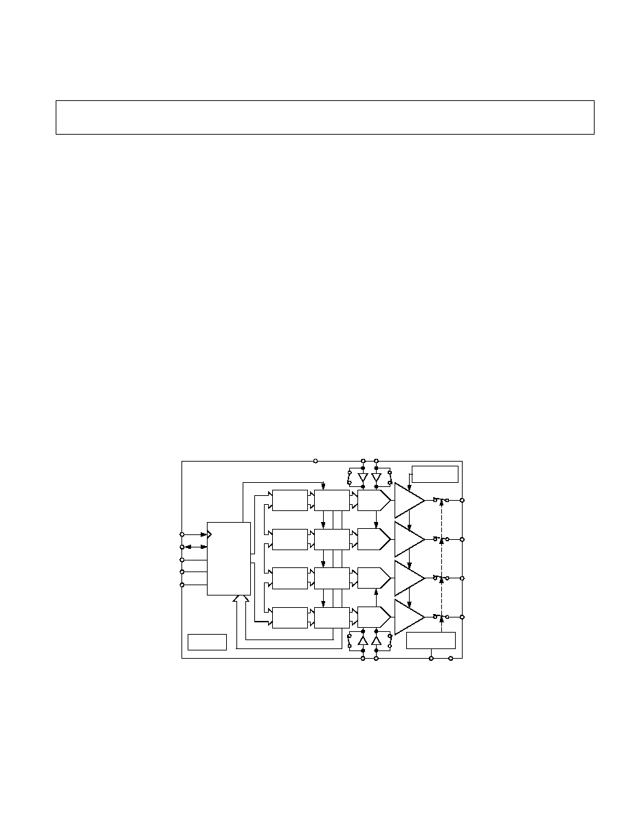
FUNCTIONAL BLOCK DIAGRAM
INPUT
REGISTER
V
OUT
A
BUFFER
STRING
DAC A
V
DD
AD5306/AD5316/AD5326
V
OUT
B
BUFFER
STRING
DAC B
V
OUT
C
BUFFER
STRING
DAC C
V
OUT
D
BUFFER
STRING
DAC D
GAIN-SELECT
LOGIC
V
REF
A
SCL
A0
PD
POWER-ON
RESET
POWER-DOWN
LOGIC
LDAC
LDAC
SDA
A1
V
REF
B
DAC
REGISTER
INPUT
REGISTER
DAC
REGISTER
INPUT
REGISTER
DAC
REGISTER
INPUT
REGISTER
DAC
REGISTER
INTERFACE
LOGIC
V
REF
D V
REF
C
GND
FEATURES
AD5306: Four Buffered 8-Bit DACs in 16-Lead TSSOP
AD5316: Four Buffered 10-Bit DACs in 16-Lead TSSOP
AD5326: Four Buffered 12-Bit DACs in 16-Lead TSSOP
Low Power Operation: 400 A @ 3 V, 500 A @ 5 V
2-Wire (I
2
C
®
-Compatible) Serial Interface
2.5 V to 5.5 V Power Supply
Guaranteed Monotonic By Design over All Codes
Power-Down to 90 nA @ 3 V, 300 nA @ 5 V (
PD Pin or Bit)
Double-Buffered Input Logic
Buffered/Unbuffered Reference Input Options
Output Range: 0V
REF
or 02 V
REF
Power-On-Reset to Zero Volts
Simultaneous Update of Outputs (
LDAC Pin)
Software Clear Facility
Data Readback Facility
On-Chip Rail-to-Rail Output Buffer Amplifiers
Temperature Range 40 C to +105 C
APPLICATIONS
Portable Battery-Powered Instruments
Digital Gain and Offset Adjustment
Programmable Voltage and Current Sources
Programmable Attenuators
Industrial Process Control
GENERAL DESCRIPTION
The AD5306/AD5316/AD5326 are quad 8-, 10-, and 12-bit
buffered voltage output DACs, in a 16-lead TSSOP package, that
operate from a single 2.5 V to 5.5 V supply, consuming 500
µA
at 3 V. Their on-chip output amplifiers allow rail-to-rail output
swing with a slew rate of 0.7 V/
µs. A 2-wire serial interface that
operates at clock rates up to 400 kHz is used. This interface is
SMBus-compatible at V
DD
< 3.6 V. Multiple devices can be placed
on the same bus.
Each DAC has a separate reference input that can be config-
ured as buffered or unbuffered. The outputs of all DACs may
be updated simultaneously using the asynchronous
LDAC input.
The parts incorporate a power-on-reset circuit that ensures that
the DAC outputs power-up to zero volts and remain there until
a valid write to the device takes place. There is also a software clear
function that clears all DACs to 0 V. The parts contain a power-
down feature that reduces the current consumption of the device
to 300 nA @ 5 V (90 nA @ 3 V).
All three parts are offered in the same pinout, which allows users
to select the amount of resolution appropriate for their applica-
tion without redesigning their circuit board.
*Protected by U.S. Patent Numbers 5,969,657 and 5,684,481.
I
2
C is a registered trademark of Philips Corporation.
2.5 V to 5.5 V, 400 A, 2-Wire Interface,
Quad Voltage Output, 8-/10-/12-Bit DACs

2
REV. B
AD5306/AD5316/AD5326SPECIFICATIONS
(V
DD
= 2.5 V to 5.5 V; V
REF
= 2 V; R
L
= 2 k
to
GND; C
L
= 200 pF to GND; all specifications T
MIN
to T
MAX
unless otherwise noted.)
B Version
2
Parameter
1
Min
Typ
Max
Unit
Conditions/Comments
DC PERFORMANCE
3, 4
AD5306
Resolution
8
Bits
Relative Accuracy
±0.15
±1
LSB
Differential Nonlinearity
±0.02
±0.25
LSB
Guaranteed Monotonic by Design over All Codes
AD5316
Resolution
10
Bits
Relative Accuracy
±0.5
±4
LSB
Differential Nonlinearity
±0.05
±0.5
LSB
Guaranteed Monotonic by Design over All Codes
AD5326
Resolution
12
Bits
Relative Accuracy
±2
±16
LSB
Differential Nonlinearity
±0.2
±1
LSB
Guaranteed Monotonic by Design over All Codes
Offset Error
±5
±60
mV
V
DD
= 4.5 V, Gain = 2; See Figures 2 and 3
Gain Error
±0.3
±1.25
% of FSR
V
DD
= 4.5 V, Gain = 2; See Figures 2 and 3
Lower Deadband
5
10
60
mV
See Figure 2; Lower Deadband Exists Only If Offset Error
Is Negative
Upper Deadband
5
10
60
mV
See Figure 3; Upper Deadband Exists Only If V
REF
= V
DD
and Offset Plus Gain Error Is Positive
Offset Error Drift
6
12
ppm of FSR/
°C
Gain Error Drift
6
5
ppm of FSR/
°C
DC Power Supply Rejection Ratio
6
60
dB
V
DD
=
±10%
DC Crosstalk
6
200
µV
R
L
= 2 k
to GND or V
DD
DAC REFERENCE INPUTS
6
V
REF
Input Range
1
V
DD
V
Buffered Reference Mode
0.25
V
DD
V
Unbuffered Reference Mode
V
REF
Input Impedance
>10
M
Buffered Reference Mode and Power-Down Mode
148
180
k
Unbuffered Reference Mode. 0V
REF
Output Range
74
90
k
Unbuffered Reference Mode. 02 V
REF
Output Range
Reference Feedthrough
90
dB
Frequency = 10 kHz
Channel-to-Channel Isolation
75
dB
Frequency = 10 kHz
OUTPUT CHARACTERISTICS
6
Minimum Output Voltage
7
0.001
V
This is a measure of the minimum and maximum drive
Maximum Output Voltage
7
V
DD
0.001
V
capability of the output amplifier.
DC Output Impedance
0.5
Short Circuit Current
25
mA
V
DD
= 5 V
16
mA
V
DD
= 3 V
Power-Up Time
2.5
µs
Coming Out of Power-Down Mode. V
DD
= 5 V
5
µs
Coming Out of Power-Down Mode. V
DD
= 3 V
LOGIC INPUTS (Excl. SCL, SDA)
6
Input Current
±1
µA
V
IL
, Input Low Voltage
0.8
V
V
DD
= 5 V
± 10%
0.6
V
V
DD
= 3 V
± 10%
0.5
V
V
DD
= 2.5 V
V
IH
, Input High Voltage
1.7
V
V
DD
= 2.5 V to 5.5 V; TTL and 1.8 V CMOS-Compatible
Pin Capacitance
3
pF
LOGIC INPUTS (SCL, SDA)
6
V
IH
, Input High Voltage
0.7 V
DD
V
DD
+ 0.3
V
SMBus-Compatible at V
DD
< 3.6 V
V
IL
, Input Low Voltage
0.3
0.3 V
DD
V
SMBus-Compatible at V
DD
< 3.6 V
I
IN
, Input Leakage Current
±1
µA
V
HYST
, Input Hysteresis
0.05 V
DD
V
See TPC 15
C
IN
, Input Capacitance
8
pF
Glitch Rejection
50
ns
Input Filtering Suppresses Noise Spikes of Less than 50 ns
LOGIC OUTPUT (SDA)
6
V
OL
, Output Low Voltage
0.4
V
I
SINK
= 3 mA
0.6
V
I
SINK
= 6 mA
Three-State Leakage Current
±1
µA
Three-State Output Capacitance
8
pF
3
REV. B
AD5306/AD5316/AD5326
B Version
2
Parameter
1
Min
Typ
Max
Unit
Conditions/Comments
POWER REQUIREMENTS
V
DD
2.5
5.5
V
I
DD
(Normal Mode)
8
V
IH
= V
DD
and V
IL
= GND. Interface Inactive
V
DD
= 4.5 V to 5.5 V
500
900
µA
All DACs in Unbuffered Mode. In Buffered Mode extra cur-
V
DD
= 2.5 V to 3.6 V
400
750
µA
rent is typically x
µA per DAC where x = 5 µA + V
REF
/R
DAC
.
I
DD
(Power-Down Mode)
V
IH
= V
DD
and V
IL
= GND. Interface Inactive
V
DD
= 4.5 V to 5.5 V
0.3
1
µA
I
DD
= 3
µA (Max) During "0" Readback on SDA
V
DD
= 2.5 V to 3.6 V
0.09
1
µA
I
DD
= 1.5
µA (Max) During "0" Readback on SDA
NOTES
1
See Terminology.
2
Temperature range: B Version: 40
°C to +105°C; typical at 25°C.
3
DC specifications tested with the outputs unloaded.
4
Linearity is tested using a reduced code range: AD5306 (Code 8 to 255); AD5316 (Code 28 to 1023); AD5326 (Code 115 to 4095).
5
This corresponds to x codes. x = Deadband Voltage/LSB size.
6
Guaranteed by design and characterization; not production tested.
7
For the amplifier output to reach its minimum voltage, Offset Error must be negative; for the amplifier output to reach its maximum voltage, V
REF
= V
DD
and Offset plus Gain
Error must be positive.
8
Interface inactive; all DACs active. DAC outputs unloaded.
Specifications subject to change without notice.
AC CHARACTERISTICS
1
B Version
3
Parameter
2
Min
Typ
Max
Unit
Conditions/Comments
Output Voltage Settling Time
V
REF
= V
DD
= 5 V
AD5306
6
8
µs
1/4 Scale to 3/4 Scale
Change
(40 Hex to C0 Hex)
AD5316
7
9
µs
1/4 Scale to 3/4 Scale
Change
(100 Hex to 300 Hex)
AD5326
8
10
µs
1/4 Scale to 3/4 Scale
Change
(400 Hex to C00 Hex)
Slew Rate
0.7
V/
µs
Major-Code Change Glitch Energy
12
nV sec
1 LSB Change Around Major Carry
Digital Feedthrough
0.5
nV sec
Digital Crosstalk
0.5
nV sec
Analog Crosstalk
1
nV sec
DAC-to-DAC Crosstalk
3
nV sec
Multiplying Bandwidth
200
kHz
V
REF
= 2 V
± 0.1 V p-p. Unbuffered Mode
Total Harmonic Distortion
70
dB
V
REF
= 2.5 V
± 0.1 V p-p. Frequency = 10 kHz
NOTES
1
Guaranteed by design and characterization; not production tested.
2
See Terminology.
3
Temperature range: B Version: 40
°C to +105°C; typical at 25°C.
Specifications subject to change without notice.
(V
DD
= 2.5 V to 5.5 V; R
L
= 2 k
to GND; C
L
= 200 pF to GND; all specifications T
MIN
to T
MAX
unless
otherwise noted.)
AD5306/AD5316/AD5326
4
REV. B
TIMING CHARACTERISTICS
1
B Version
Parameter
2
Limit at T
MIN
, T
MAX
Unit
Conditions/Comments
f
SCL
400
kHz max
SCL Clock Frequency
t
1
2.5
µs min
SCL Cycle Time
t
2
0.6
µs min
t
HIGH
, SCL High Time
t
3
1.3
µs min
t
LOW
, SCL Low Time
t
4
0.6
µs min
t
HD,STA
, Start/Repeated Start Condition Hold Time
t
5
100
ns min
t
SU,DAT
, Data Setup Time
t
6
3
0.9
µs max
t
HD,DAT
, Data Hold Time
0
µs min
t
7
0.6
µs min
t
SU,STA
, Setup Time for Repeated Start
t
8
0.6
µs min
t
SU,STO
, Stop Condition Setup Time
t
9
1.3
µs min
t
BUF
, Bus Free Time Between a STOP and a START Condition
t
10
300
ns max
t
R
, Rise Time of SCL and SDA when Receiving
0
ns min
t
R
, Rise Time of SCL and SDA when Receiving (CMOS-Compatible)
t
11
250
ns max
t
F
, Fall Time of SDA when Transmitting
0
ns min
t
F
, Fall Time of SDA when Receiving (CMOS-Compatible)
300
ns max
t
F
, Fall Time of SCL and SDA when Receiving
20 + 0.1C
b
4
ns min
t
F
, Fall Time of SCL and SDA when Transmitting
t
12
20
ns min
LDAC Pulsewidth
t
13
400
ns min
SCL Rising Edge to
LDAC Rising Edge
C
b
400
pF max
Capacitive Load for Each Bus Line
NOTES
1
See Figure 1.
2
Guaranteed by design and characterization; not production tested.
3
A master device must provide a hold time of at least 300 ns for the SDA signal (referred to the V
IH
min of the SCL signal) in order to bridge the undefined region of
SCL's falling edge.
4
C
b
is the total capacitance of one bus line in pF. t
R
and t
F
measured between 0.3 V
DD
and 0.7 V
DD
.
Specifications subject to change without notice.
SCL
SDA
t
9
t
4
t
6
t
2
t
5
t
7
t
8
t
1
t
11
t
10
t
3
t
12
LDAC
1
LDAC
2
START
CONDITION
REPEATED START
CONDITION
STOP
CONDITION
NOTES
1
ASYNCHRONOUS
LDAC UPDATE MODE.
2
SYNCHRONOUS
LDAC UPDATE MODE.
t
4
t
12
t
13
Figure 1. 2-Wire Serial Interface Timing Diagram
(V
DD
= 2.5 V to 5.5 V; all specifications T
MIN
to T
MAX
unless otherwise noted.)
AD5306/AD5316/AD5326
5
REV. B
ABSOLUTE MAXIMUM RATINGS
1, 2
(T
A
= 25
°C unless otherwise noted)
V
DD
to GND . . . . . . . . . . . . . . . . . . . . . . . . . . 0.3 V to +7 V
SCL, SDA to GND . . . . . . . . . . . . . . . 0.3 V to V
DD
+ 0.3 V
A0, A1,
LDAC, PD to GND . . . . . . . . 0.3 V to V
DD
+ 0.3 V
Reference Input Voltage to GND . . . . 0.3 V to V
DD
+ 0.3 V
V
OUT
AD to GND . . . . . . . . . . . . . . . 0.3 V to V
DD
+ 0.3 V
Operating Temperature Range
Industrial (B Version) . . . . . . . . . . . . . . . 40
°C to +105°C
Storage Temperature Range . . . . . . . . . . . . 65
°C to +150°C
Junction Temperature (T
J
max) . . . . . . . . . . . . . . . . . . 150
°C
16-Lead TSSOP Package
Power Dissipation . . . . . . . . . . . . . . . . . . (T
J
max T
A
)/
JA
JA
Thermal Impedance . . . . . . . . . . . . . . . . . . 150.4
°C/W
CAUTION
ESD (electrostatic discharge) sensitive device. Electrostatic charges as high as 4000 V readily
accumulate on the human body and test equipment and can discharge without detection. Although
the AD5306/AD5316/AD5326 features proprietary ESD protection circuitry, permanent damage
may occur on devices subjected to high-energy electrostatic discharges. Therefore, proper ESD
precautions are recommended to avoid performance degradation or loss of functionality.
WARNING!
ESD SENSITIVE DEVICE
Reflow Soldering
Peak Temperature . . . . . . . . . . . . . . . . . . . . . 220 +5/0
°C
Time at Peak Temperature . . . . . . . . . . . . 10 sec to 40 sec
NOTES
1
Stresses above those listed under Absolute Maximum Ratings may cause perma-
nent damage to the device. This is a stress rating only; and functional operation of
the device at these or any other conditions above those listed in the operational
sections of this specification is not implied. Exposure to absolute maximum rating
conditions for extended periods may affect device reliability.
2
Transient currents of up to 100 mA will not cause SCR latch-up.
ORDERING GUIDE
Model
Temperature Range
Package Description
Package Option
AD5306BRU
40
°C to +105°C
Thin Shrink Small Outline Package (TSSOP)
RU-16
AD5316BRU
40
°C to +105°C
Thin Shrink Small Outline Package (TSSOP)
RU-16
AD5326BRU
40
°C to +105°C
Thin Shrink Small Outline Package (TSSOP)
RU-16