 | –≠–ª–µ–∫—Ç—Ä–æ–Ω–Ω—ã–π –∫–æ–º–ø–æ–Ω–µ–Ω—Ç: AD5320BRM | –°–∫–∞—á–∞—Ç—å:  PDF PDF  ZIP ZIP |
REV. B
Information furnished by Analog Devices is believed to be accurate and
reliable. However, no responsibility is assumed by Analog Devices for its
use, nor for any infringements of patents or other rights of third parties
which may result from its use. No license is granted by implication or
otherwise under any patent or patent rights of Analog Devices.
a
AD5320*
One Technology Way, P.O. Box 9106, Norwood, MA 02062-9106, U.S.A.
Tel: 781/329-4700
World Wide Web Site: http://www.analog.com
Fax: 781/326-8703
© Analog Devices, Inc., 2000
+2.7 V to +5.5 V, 140 A, Rail-to-Rail Output
12-Bit DAC in a SOT-23
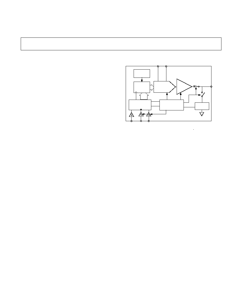
FUNCTIONAL BLOCK DIAGRAM
POWER-ON
RESET
DAC
REGISTER
12-BIT
DAC
INPUT
CONTROL
LOGIC
POWER-DOWN
CONTROL LOGIC
AD5320
V
DD
GND
REF (+) REF (≠)
RESISTOR
NETWORK
V
OUT
SYNC
SCLK
DIN
OUTPUT
BUFFER
FEATURES
Single 12-Bit DAC
6-Lead SOT-23 and 8-Lead SOIC Packages
Micropower Operation: 140 A @ 5 V
Power-Down to 200 nA @ 5 V, 50 nA @ 3 V
+2.7 V to +5.5 V Power Supply
Guaranteed Monotonic by Design
Reference Derived from Power Supply
Power-On-Reset to Zero Volts
Three Power-Down Functions
Low Power Serial Interface with Schmitt-Triggered
Inputs
On-Chip Output Buffer Amplifier, Rail-to-Rail Operation
SYNC Interrupt Facility
APPLICATIONS
Portable Battery Powered Instruments
Digital Gain and Offset Adjustment
Programmable Voltage and Current Sources
Programmable Attenuators
GENERAL DESCRIPTION
The AD5320 is a single, 12-bit buffered voltage out DAC that
operates from a single +2.7 V to +5.5 V supply consuming
115
µ
A at 3 V. Its on-chip precision output amplifier allows
rail-to-rail output swing to be achieved. The AD5320 utilizes a
versatile three-wire serial interface that operates at clock rates up
to 30 MHz and is compatible with standard SPITM, QSPITM,
MICROWIRETM and DSP interface standards.
The reference for AD5320 is derived from the power supply
inputs and thus gives the widest dynamic output range. The part
incorporates a power-on-reset circuit that ensures that the DAC
output powers up to zero volts and remains there until a valid
write takes place to the device. The part contains a power-down
feature that reduces the current consumption of the device to
200 nA at 5 V and provides software selectable output loads
while in power-down mode. The part is put into power-down
mode over the serial interface.
The low power consumption of this part in normal operation
makes it ideally suited to portable battery operated equipment.
The power consumption is 0.7 mW at 5 V reducing to 1
µ
W in
power-down mode.
The AD5320 is one of a family of pin-compatible DACs. The
AD5300 is the 8-bit version and the AD5310 is the 10-bit
version. The AD5300/AD5310/AD5320 are available in 6-lead
SOT-23 packages and 8-lead
µ
SOIC packages.
PRODUCT HIGHLIGHTS
1. Available in 6-lead SOT-23 and 8-lead
µ
SOIC packages.
2. Low power, single supply operation. This part operates from
a single +2.7 V to +5.5 V supply and typically consumes
0.35 mW at 3 V and 0.7 mW at 5 V, making it ideal for
battery powered applications.
3. The on-chip output buffer amplifier allows the output of the
DAC to swing rail-to-rail with a slew rate of 1 V/
µ
s.
4. Reference derived from the power supply.
5. High speed serial interface with clock speeds up to 30 MHz.
Designed for very low power consumption. The interface
only powers up during a write cycle.
6. Power-down capability. When powered down, the DAC
typically consumes 50 nA at 3 V and 200 nA at 5 V.
SPI and QSPI are trademarks of Motorola, Inc.
MICROWIRE is a trademark of National Semiconductor Corporation.
*Patent pending; protected by U.S. Patent No. 5684481.

≠2≠
REV. B
AD5320≠SPECIFICATIONS
(V
DD
= +2.7 V to +5.5 V; R
L
= 2 k
to GND; C
L
= 200 pF to GND; all specifications
T
MIN
to T
MAX
unless otherwise noted)
B Version
1
Parameter
Min
Typ
Max
Unit
Conditions/Comments
STATIC PERFORMANCE
2
Resolution
12
Bits
Relative Accuracy
±
16
LSB
See Figure 2.
Differential Nonlinearity
±
1
LSB
Guaranteed Monotonic by Design. See Figure 3.
Zero Code Error
+5
+40
mV
All Zeroes Loaded to DAC Register. See Figure 6.
Full-Scale Error
≠0.15
≠1.25
% of FSR
All Ones Loaded to DAC Register. See Figure 6.
Gain Error
±
1.25
% of FSR
Zero Code Error Drift
≠20
µ
V/
∞
C
Gain Temperature Coefficient
≠5
ppm of FSR/
∞
C
OUTPUT CHARACTERISTICS
3
Output Voltage Range
0
V
DD
V
Output Voltage Settling Time
8
10
µ
s
1/4 Scale to 3/4 Scale Change (400 Hex to C00 Hex).
R
L
= 2 k
; 0 pF < C
L
< 200 pF. See Figure 16.
12
µ
s
R
L
= 2 k
; C
L
= 500 pF
Slew Rate
1
V/
µ
s
Capacitive Load Stability
470
pF
R
L
=
1000
pF
R
L
= 2 k
Digital-to-Analog Glitch Impulse
20
nV-s
1 LSB Change Around Major Carry. See Figure 19.
Digital Feedthrough
0.5
nV-s
DC Output Impedance
1
Short Circuit Current
50
mA
V
DD
= +5 V
20
mA
V
DD
= +3 V
Power-Up Time
2.5
µ
s
Coming Out of Power-Down Mode. V
DD
= +5 V
5
µ
s
Coming Out of Power-Down Mode. V
DD
= +3 V
LOGIC INPUTS
3
Input Current
±
1
µ
A
V
INL
, Input Low Voltage
0.8
V
V
DD
= +5 V
V
INL
, Input Low Voltage
0.6
V
V
DD
= +3 V
V
INH
, Input High Voltage
2.4
V
V
DD
= +5 V
V
INH
, Input High Voltage
2.1
V
V
DD
= +3 V
Pin Capacitance
3
pF
POWER REQUIREMENTS
V
DD
2.7
5.5
V
I
DD
(Normal Mode)
DAC Active and Excluding Load Current
V
DD
= +4.5 V to +5.5 V
140
250
µ
A
V
IH
= V
DD
and V
IL
= GND
V
DD
= +2.7 V to +3.6 V
115
200
µ
A
V
IH
= V
DD
and V
IL
= GND
I
DD
(All Power-Down Modes)
V
DD
= +4.5 V to +5.5 V
0.2
1
µ
A
V
IH
= V
DD
and V
IL
= GND
V
DD
= +2.7 V to +3.6 V
0.05
1
µ
A
V
IH
= V
DD
and V
IL
= GND
POWER EFFICIENCY
I
OUT
/I
DD
93
%
I
LOAD
= 2 mA. V
DD
= +5 V
NOTES
1
Temperature ranges are as follows: B Version: ≠40
∞
C to +105
∞
C.
2
Linearity calculated using a reduced code range of 48 to 4047. Output unloaded.
3
Guaranteed by design and characterization, not production tested.
Specifications subject to change without notice.

AD5320
≠3≠
REV. B
TIMING CHARACTERISTICS
1, 2
Limit at T
MIN
, T
MAX
Parameter
V
DD
= 2.7 V to 3.6 V
V
DD
= 3.6 V to 5.5 V
Unit
Conditions/Comments
t
1
3
50
33
ns min
SCLK Cycle Time
t
2
13
13
ns min
SCLK High Time
t
3
22.5
13
ns min
SCLK Low Time
t
4
0
0
ns min
SYNC to SCLK Rising Edge Setup Time
t
5
5
5
ns min
Data Setup Time
t
6
4.5
4.5
ns min
Data Hold Time
t
7
0
0
ns min
SCLK Falling Edge to
SYNC Rising Edge
t
8
50
33
ns min
Minimum
SYNC High Time
NOTES
1
All input signals are specified with tr = tf = 5 ns (10% to 90% of V
DD
) and timed from a voltage level of (V
IL
+ V
IH
)/2.
2
See Figure 1.
3
Maximum SCLK frequency is 30 MHz at V
DD
= +3.6 V to +5.5 V and 20 MHz at V
DD
= +2.7 V to +3.6 V.
Specifications subject to change without notice.
SCLK
SYNC
DIN
t
1
t
2
t
3
t
5
t
6
t
7
t
8
t
4
DB15
DB0
Figure 1. Serial Write Operation
(V
DD
= +2.7 V to +5.5 V; all specifications T
MIN
to T
MAX
unless otherwise noted)
ABSOLUTE MAXIMUM RATINGS*
(T
A
= +25
∞
C unless otherwise noted)
V
DD
to GND . . . . . . . . . . . . . . . . . . . . . . . . . . ≠0.3 V to +7 V
Digital Input Voltage to GND . . . . . . . . ≠0.3 V to V
DD
+ 0.3 V
V
OUT
to GND . . . . . . . . . . . . . . . . . . . ≠0.3 V to V
DD
+ 0.3 V
Operating Temperature Range
Industrial (B Version) . . . . . . . . . . . . . . . ≠40
∞
C to +105
∞
C
Storage Temperature Range . . . . . . . . . . . . ≠65
∞
C to +150
∞
C
Junction Temperature (T
J
Max) . . . . . . . . . . . . . . . . . +150
∞
C
SOT-23 Package
Power Dissipation . . . . . . . . . . . . . . . . . . . (T
J
Max≠T
A
)/
JA
JA
Thermal Impedance . . . . . . . . . . . . . . . . . . . . 240
∞
C/W
Lead Temperature, Soldering
Vapor Phase (60 sec) . . . . . . . . . . . . . . . . . . . . . . +215
∞
C
Infrared (15 sec) . . . . . . . . . . . . . . . . . . . . . . . . . . +220
∞
C
µ
SOIC Package . . . . . . . . . . . . . . . . . . . . . . . . . . . . . 450 mW
Power Dissipation . . . . . . . . . . . . . . . . . . . (T
J
Max≠T
A
)/
JA
JA
Thermal Impedance . . . . . . . . . . . . . . . . . . . . 206
∞
C/W
JC
Thermal Impedance . . . . . . . . . . . . . . . . . . . . . 44
∞
C/W
Lead Temperature, Soldering
Vapor Phase (60 sec) . . . . . . . . . . . . . . . . . . . . . . +215
∞
C
Infrared (15 sec) . . . . . . . . . . . . . . . . . . . . . . . . . . +220
∞
C
*Stresses above those listed under Absolute Maximum Ratings may cause perma-
nent damage to the device. This is a stress rating only; functional operation of the
device at these or any other conditions above those listed in the operational sections
of this specification is not implied. Exposure to absolute maximum rating condi-
tions for extended periods may affect device reliability.
ORDERING GUIDE
Temperature
Branding
Package
Model
Range
Information Options*
AD5320BRT
≠40
∞
C to +105
∞
C
D4B
RT-6
AD5320BRM
≠40
∞
C to +105
∞
C
D4B
RM-8
*RT = SOT-23; RM =
µ
SOIC.
CAUTION
ESD (electrostatic discharge) sensitive device. Electrostatic charges as high as 4000 V readily
accumulate on the human body and test equipment and can discharge without detection.
Although the AD5320 features proprietary ESD protection circuitry, permanent damage may
occur on devices subjected to high-energy electrostatic discharges. Therefore, proper ESD
precautions are recommended to avoid performance degradation or loss of functionality.
WARNING!
ESD SENSITIVE DEVICE

AD5320
≠4≠
REV. B
PIN CONFIGURATIONS
TOP VIEW
(Not to Scale)
6
5
4
1
2
3
V
OUT
GND
V
DD
SYNC
SCLK
DIN
AD5320
TOP VIEW
(Not to Scale)
8
7
6
5
1
2
3
4
NC
AD5320
SYNC
V
OUT
GND
V
DD
SCLK
DIN
NC
SOT-23
SOIC
NC = NO CONNECT
PIN FUNCTION DESCRIPTIONS
SOT-23 Pin Numbers
Pin
No.
Mnemonic
Function
1
V
OUT
Analog output voltage from DAC. The output amplifier has rail-to-rail operation.
2
GND
Ground reference point for all circuitry on the part.
3
V
DD
Power Supply Input. These parts can be operated from +2.5 V to +5.5 V and V
DD
should be de-
coupled to GND.
4
DIN
Serial Data Input. This device has a 16-bit shift register. Data is clocked into the register on the
falling edge of the serial clock input.
5
SCLK
Serial Clock Input. Data is clocked into the input shift register on the falling edge of the serial clock
input. Data can be transferred at rates up to 30 MHz.
6
SYNC
Level triggered control input (active low). This is the frame synchronization signal for the input
data. When
SYNC goes low, it enables the input shift register and data is transferred in on the
falling edges of the following clocks. The DAC is updated following the 16th clock cycle unless
SYNC is taken high before this edge in which case the rising edge of SYNC acts as an interrupt and
the write sequence is ignored by the DAC.

AD5320
≠5≠
REV. B
TERMINOLOGY
Relative Accuracy
For the DAC, relative accuracy or Integral Nonlinearity (INL)
is a measure of the maximum deviation, in LSBs, from a straight
line passing through the endpoints of the DAC transfer func-
tion. A typical INL vs. code plot can be seen in Figure 2.
Differential Nonlinearity
Differential Nonlinearity (DNL) is the difference between the
measured change and the ideal 1 LSB change between any two
adjacent codes. A specified differential nonlinearity of
±
1 LSB
maximum ensures monotonicity. This DAC is guaranteed
monotonic by design. A typical DNL vs. code plot can be seen
in Figure 3.
Zero-Code Error
Zero-code error is a measure of the output error when zero code
(000 Hex) is loaded to the DAC register. Ideally the output
should be 0 V. The zero-code error is always positive in the
AD5320 because the output of the DAC cannot go below 0 V.
It is due to a combination of the offset errors in the DAC and
output amplifier. Zero-code error is expressed in mV. A plot of
zero-code error vs. temperature can be seen in Figure 6.
Full-Scale Error
Full-scale error is a measure of the output error when full-scale
code (FFF Hex) is loaded to the DAC register. Ideally the
output should be V
DD
≠ 1 LSB. Full-scale error is expressed in
percent of full-scale range. A plot of full-scale error vs. tempera-
ture can be seen in Figure 6.
Gain Error
This is a measure of the span error of the DAC. It is the devia-
tion in slope of the DAC transfer characteristic from ideal
expressed as a percent of the full-scale range.
Total Unadjusted Error
Total Unadjusted Error (TUE) is a measure of the output error
taking all the various errors into account. A typical TUE vs.
code plot can be seen in Figure 4.
Zero-Code Error Drift
This is a measure of the change in zero-code error with a
change in temperature. It is expressed in
µ
V/
∞
C.
Gain Error Drift
This is a measure of the change in gain error with changes in
temperature. It is expressed in (ppm of full-scale range)/
∞
C.
Digital-to-Analog Glitch Impulse
Digital-to-analog glitch impulse is the impulse injected into the
analog output when the input code in the DAC register changes
state. It is normally specified as the area of the glitch in nV secs
and is measured when the digital input code is changed by
1 LSB at the major carry transition (7FF Hex to 800 Hex). See
Figure 19.
Digital Feedthrough
Digital feedthrough is a measure of the impulse injected into the
analog output of the DAC from the digital inputs of the DAC
but is measured when the DAC output is not updated. It is
specified in nV secs and measured with a full-scale code
change on the data bus, i.e., from all 0s to all 1s and vice versa.