 | ÐлекÑÑоннÑй компоненÑ: AD5342BRU | СкаÑаÑÑ:  PDF PDF  ZIP ZIP |
Äîêóìåíòàöèÿ è îïèñàíèÿ www.docs.chipfind.ru
REV. 0
Information furnished by Analog Devices is believed to be accurate and
reliable. However, no responsibility is assumed by Analog Devices for its
use, nor for any infringements of patents or other rights of third parties
which may result from its use. No license is granted by implication or
otherwise under any patent or patent rights of Analog Devices.
a
AD5332/AD5333/AD5342/AD5343*
One Technology Way, P.O. Box 9106, Norwood, MA 02062-9106, U.S.A.
Tel: 781/329-4700
World Wide Web Site: http://www.analog.com
Fax: 781/326-8703
© Analog Devices, Inc., 2000
2.5 V to 5.5 V, 230 A, Parallel Interface
Dual Voltage-Output 8-/10-/12-Bit DACs
AD5332 FUNCTIONAL BLOCK DIAGRAM
(Other Diagrams Inside)
POWER-ON
RESET
DAC
REGISTER
DAC
REGISTER
INPUT
REGISTER
INPUT
REGISTER
INTER-
FACE
LOGIC
DB
7
DB
0
CS
WR
A0
CLR
LDAC
.
.
.
V
REF
A
RESET
V
REF
B
V
OUT
A
BUFFER
AD5332
V
OUT
B
BUFFER
V
DD
POWER-DOWN
LOGIC
PD GND
8-BIT
DAC
8-BIT
DAC
FEATURES
AD5332: Dual 8-Bit DAC in 20-Lead TSSOP
AD5333: Dual 10-Bit DAC in 24-Lead TSSOP
AD5342: Dual 12-Bit DAC in 28-Lead TSSOP
AD5343: Dual 12-Bit DAC in 20-Lead TSSOP
Low Power Operation: 230 A @ 3 V, 300 A @ 5 V
via
PD Pin
Power-Down to 80 nA @ 3 V, 200 nA @ 5 V
2.5 V to 5.5 V Power Supply
Double-Buffered Input Logic
Guaranteed Monotonic by Design Over All Codes
Buffered/Unbuffered Reference Input Options
Output Range: 0V
REF
or 02 V
REF
Power-On Reset to Zero Volts
Simultaneous Update of DAC Outputs via
LDAC Pin
Asynchronous
CLR Facility
Low Power Parallel Data Interface
On-Chip Rail-to-Rail Output Buffer Amplifiers
Temperature Range: 40 C to +105 C
APPLICATIONS
Portable Battery-Powered Instruments
Digital Gain and Offset Adjustment
Programmable Voltage and Current Sources
Programmable Attenuators
Industrial Process Control
GENERAL DESCRIPTION
The AD5332/AD5333/AD5342/AD5343 are dual 8-, 10-, and
12-bit DACs. They operate from a 2.5 V to 5.5 V supply con-
suming just 230
µA at 3 V, and feature a power-down pin, PD
that further reduces the current to 80 nA. These devices incor-
porate an on-chip output buffer that can drive the output to
both supply rails, while the AD5333 and AD5342 allow a choice
of buffered or unbuffered reference input.
The AD5332/AD5333/AD5342/AD5343 have a parallel interface.
CS selects the device and data is loaded into the input registers
on the rising edge of WR.
The GAIN pin on the AD5333 and AD5342 allows the output
range to be set at 0 V to V
REF
or 0 V to 2
× V
REF
.
Input data to the DACs is double-buffered, allowing simultaneous
update of multiple DACs in a system using the LDAC pin.
An asynchronous CLR input is also provided, which resets the
contents of the Input Register and the DAC Register to all zeros.
These devices also incorporate a power-on reset circuit that ensures
that the DAC output powers on to 0 V and remains there until
valid data is written to the device.
The AD5332/AD5333/AD5342/AD5343 are available in Thin
Shrink Small Outline Packages (TSSOP).
*Protected by U.S. Patent Number 5,969,657; other patents pending.

REV. 0
2
AD5332/AD5333/AD5342/AD5343SPECIFICATIONS
(V
DD
= 2.5 V to 5.5 V, V
REF
= 2 V. R
L
= 2 k
to GND; C
L
=200 pF to GND; all specifications T
MIN
to T
MAX
unless otherwise noted.)
B Version
2
Parameter
1
Min
Typ
Max
Unit
Conditions/Comments
DC PERFORMANCE
3, 4
AD5332
Resolution
8
Bits
Relative Accuracy
±0.15
±1
LSB
Differential Nonlinearity
±0.02
±0.25
LSB
Guaranteed Monotonic By Design Over All Codes
AD5333
Resolution
10
Bits
Relative Accuracy
±0.5
±4
LSB
Differential Nonlinearity
±0.05
±0.5
LSB
Guaranteed Monotonic By Design Over All Codes
AD5342/AD5343
Resolution
12
Bits
Relative Accuracy
±2
±16
LSB
Differential Nonlinearity
±0.2
±1
LSB
Guaranteed Monotonic By Design Over All Codes
Offset Error
±0.4
±3
% of FSR
Gain Error
±0.15
±1
% of FSR
Lower Deadband
5
10
60
mV
Lower Deadband Exists Only if Offset Error Is Negative
Upper Deadband
10
60
mV
V
DD
= 5 V. Upper Deadband Exists Only if V
REF =
V
DD
Offset Error Drift
6
12
ppm of FSR/
°C
Gain Error Drift
6
5
ppm of FSR/
°C
DC Power Supply Rejection Ratio
6
60
dB
V
DD
=
±10%
DC Crosstalk
6
200
µV
R
L
= 2 k
to GND, 2 k to V
DD
; C
L
= 200 pF to GND;
Gain = 0
DAC REFERENCE INPUT
6
V
REF
Input Range
1
V
DD
V
Buffered Reference (AD5333 and AD5342)
0.25
V
DD
V
Unbuffered Reference
V
REF
Input Impedance
>10
M
Buffered Reference (AD5333 and AD5342)
180
k
Unbuffered Reference. Gain = 1, Input Impedance = R
DAC
90
k
Unbuffered Reference. Gain = 2, Input Impedance = R
DAC
Reference Feedthrough
90
dB
Frequency = 10 kHz
Channel-to-Channel Isolation
90
dB
Frequency = 10 kHz (AD5332, AD5333, and AD5342)
OUTPUT CHARACTERISTICS
6
Minimum Output Voltage
4, 7
0.001
V min
Rail-to-Rail Operation
Maximum Output Voltage
4, 7
V
DD
0.001
V max
DC Output Impedance
0.5
Short Circuit Current
25
mA
V
DD
= 5 V
16
mA
V
DD
= 3 V
Power-Up Time
2.5
µs
Coming Out of Power-Down Mode. V
DD
= 5 V
5
µs
Coming Out of Power-Down Mode. V
DD
= 3 V
LOGIC INPUTS
6
Input Current
±1
µA
V
IL
, Input Low Voltage
0.8
V
V
DD
= 5 V
± 10%
0.6
V
V
DD
= 3 V
± 10%
0.5
V
V
DD
= 2.5 V
V
IH
, Input High Voltage
2.4
V
V
DD
= 5 V
± 10%
2.1
V
V
DD
= 3 V
± 10%
2.0
V
V
DD
= 2.5 V
Pin Capacitance
3.5
pF
POWER REQUIREMENTS
V
DD
2.5
5.5
V
I
DD
(Normal Mode)
All DACs active and excluding load currents
V
DD
= 4.5 V to 5.5 V
300
450
µA
Unbuffered Reference. V
IH
= V
DD
, V
IL
= GND.
V
DD
= 2.5 V to 3.6 V
230
350
µA
I
DD
increases by 50
µA at V
REF
> V
DD
100 mV.
In Buffered Mode extra current is (5 +V
REF
/R
DAC
)
µA.
I
DD
(Power-Down Mode)
V
DD
= 4.5 V to 5.5 V
0.2
1
µA
V
DD
= 2.5 V to 3.6 V
0.08
1
µA
NOTES
1
See Terminology section.
2
Temperature range: B Version: 40
°C to +105°C; typical specifications are at 25°C.
3
Linearity is tested using a reduced code range: AD5332 (Code 8 to 255); AD5333 (Code 28 to 1023); AD5342/AD5343 (Code 115 to 4095).
4
DC specifications tested with outputs unloaded.
5
This corresponds to x codes. x = Deadband voltage/LSB size.
6
Guaranteed by design and characterization, not production tested.
7
In order for the amplifier output to reach its minimum voltage, Offset Error must be negative. In order for the amplifier output to reach its maximum voltage, V
REF
= V
DD
and
"Offset plus Gain" Error must be positive.
Specifications subject to change without notice.
REV. 0
3
AD5332/AD5333/AD5342/AD5343
AC CHARACTERISTICS
1
B Version
3
Parameter
2
Min
Typ
Max
Unit
Conditions/Comments
Output Voltage Settling Time
V
REF
= 2 V. See Figure 20
AD5332
6
8
µs
1/4 Scale to 3/4 Scale Change (40 H to C0 H)
AD5333
7
9
µs
1/4 Scale to 3/4 Scale Change (100 H to 300 H)
AD5342
8
10
µs
1/4 Scale to 3/4 Scale Change (400 H to C00 H)
AD5343
8
10
µs
1/4 Scale to 3/4 Scale Change (400 H to C00 H)
Slew Rate
0.7
V/
µs
Major Code Transition Glitch Energy
6
nV-s
1 LSB Change Around Major Carry
Digital Feedthrough
0.5
nV-s
Digital Crosstalk
3
nV-s
Analog Crosstalk
0.5
nV-s
DAC-to-DAC Crosstalk
3.5
nV-s
Multiplying Bandwidth
200
kHz
V
REF
= 2 V
± 0.1 V p-p. Unbuffered Mode
Total Harmonic Distortion
70
dB
V
REF
= 2.5 V
± 0.1 V p-p. Frequency = 10 kHz
NOTES
1
Guaranteed by design and characterization, not production tested.
2
See Terminology section.
3
Temperature range: B Version: 40
°C to +105°C; typical specifications are at 25°C.
Specifications subject to change without notice.
TIMING CHARACTERISTICS
1, 2, 3
Parameter
Limit at T
MIN
, T
MAX
Unit
Condition/Comments
t
1
0
ns min
CS to WR Setup Time
t
2
0
ns min
CS to WR Hold Time
t
3
20
ns min
WR Pulsewidth
t
4
5
ns min
Data, GAIN, BUF, HBEN Setup Time
t
5
4.5
ns min
Data, GAIN, BUF, HBEN Hold Time
t
6
5
ns min
Synchronous Mode. WR Falling to LDAC Falling
t
7
5
ns min
Synchronous Mode. LDAC Falling to WR Rising
t
8
4.5
ns min
Synchronous Mode. WR Rising to LDAC Rising
t
9
5
ns min
Asynchronous Mode. LDAC Rising to WR Rising
t
10
4.5
ns min
Asynchronous Mode. WR Rising to LDAC Falling
t
11
20
ns min
LDAC Pulsewidth
t
12
20
ns min
CLR Pulsewidth
t
13
50
ns min
Time Between WR Cycles
t
14
20
ns min
A0 Setup Time
t
15
0
ns min
A0 Hold Time
NOTES
1
Guaranteed by design and characterization, not production tested.
2
All input signals are specified with tr = tf = 5 ns (10% to 90% of V
DD
) and
timed from a voltage level of (V
IL
+ V
IH
)/2.
3
See Figure 1.
Specifications subject to change without notice.
(V
DD
= 2.5 V to 5.5 V. R
L
= 2 k
to GND; C
L
= 200 pF to GND; all specifications T
MIN
to T
MAX
unless
otherwise noted.)
t
4
t
13
t
7
t
14
t
15
CS
WR
DATA,
GAIN,
BUF,
HBEN
LDAC
1
LDAC
2
CLR
1
SYNCHRONOUS
LDAC UPDATE MODE
2
ASYNCHRONOUS
LDAC UPDATE MODE
A0
t
1
t
2
t
3
t
5
t
6
t
8
t
9
t
10
t
11
t
12
Figure 1. Parallel Interface Timing Diagram
(V
DD
= 2.5 V to 5.5 V, All specifications T
MIN
to T
MAX
unless otherwise noted.)
REV. 0
AD5332/AD5333/AD5342/AD5343
4
CAUTION
ESD (electrostatic discharge) sensitive device. Electrostatic charges as high as 4000 V readily
accumulate on the human body and test equipment and can discharge without detection. Although
the AD5332/AD5333/AD5342/AD5343 features proprietary ESD protection circuitry, permanent
damage may occur on devices subjected to high-energy electrostatic discharges. Therefore, proper
ESD precautions are recommended to avoid performance degradation or loss of functionality.
WARNING!
ESD SENSITIVE DEVICE
ABSOLUTE MAXIMUM RATINGS
*
(T
A
= 25
°C unless otherwise noted)
V
DD
to GND . . . . . . . . . . . . . . . . . . . . . . . . . . 0.3 V to +7 V
Digital Input Voltage to GND . . . . . . . 0.3 V to V
DD
+ 0.3 V
Digital Output Voltage to GND . . . . . 0.3 V to V
DD
+ 0.3 V
Reference Input Voltage to GND . . . . 0.3 V to V
DD
+ 0.3 V
V
OUT
to GND . . . . . . . . . . . . . . . . . . . 0.3 V to V
DD
+ 0.3 V
Operating Temperature Range
Industrial (B Version) . . . . . . . . . . . . . . . 40
°C to +105°C
Storage Temperature Range . . . . . . . . . . . . 65
°C to +150°C
Junction Temperature . . . . . . . . . . . . . . . . . . . . . . . . . 150
°C
TSSOP Package
Power Dissipation . . . . . . . . . . . . . . . (T
J
max T
A
)/
JA
mW
JA
Thermal Impedance (20-Lead TSSOP) . . . . . 143
°C/W
JA
Thermal Impedance (24-Lead TSSOP) . . . . . 128
°C/W
JA
Thermal Impedance (28-Lead TSSOP) . . . . 97.9
°C/W
JC
Thermal Impedance (20-Lead TSSOP) . . . . . . 45
°C/W
JC
Thermal Impedance (24-Lead TSSOP) . . . . . . 42
°C/W
JC
Thermal Impedance (28-Lead TSSOP) . . . . . . 14
°C/W
Reflow Soldering
Peak Temperature . . . . . . . . . . . . . . . . . . . . . 220 +5/0
°C
Time at Peak Temperature . . . . . . . . . . . . 10 sec to 40 sec
*Stresses above those listed under Absolute Maximum Ratings may cause perma-
nent damage to the device. This is a stress rating only; functional operation of the
device at these or any other conditions above those listed in the operational
sections of this specification is not implied. Exposure to absolute maximum rating
conditions for extended periods may affect device reliability.
ORDERING GUIDE
Package
Model
Temperature Range
Package Description
Option
AD5332BRU
40
°C to +105°C
TSSOP (Thin Shrink Small Outline Package)
RU-20
AD5333BRU
40
°C to +105°C
TSSOP (Thin Shrink Small Outline Package)
RU-24
AD5342BRU
40
°C to +105°C
TSSOP (Thin Shrink Small Outline Package)
RU-28
AD5343BRU
40
°C to +105°C
TSSOP (Thin Shrink Small Outline Package)
RU-20
REV. 0
AD5332/AD5333/AD5342/AD5343
5
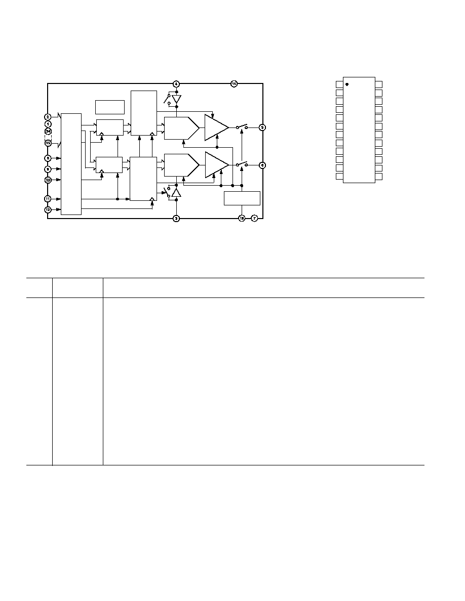
AD5332 FUNCTIONAL BLOCK DIAGRAM
POWER-ON
RESET
DAC
REGISTER
DAC
REGISTER
INPUT
REGISTER
INPUT
REGISTER
INTER-
FACE
LOGIC
DB
7
DB
0
CS
WR
A0
CLR
LDAC
.
.
.
V
REF
A
RESET
V
REF
B
V
OUT
A
BUFFER
AD5332
V
OUT
B
BUFFER
V
DD
POWER-DOWN
LOGIC
PD GND
8-BIT
DAC
8-BIT
DAC
AD5332 PIN FUNCTION DESCRIPTIONS
Pin
No.
Mnemonic
Function
1
V
REF
B
Unbuffered reference input for DAC B.
2
V
REF
A
Unbuffered reference input for DAC A.
3
V
OUT
A
Output of DAC A. Buffered output with rail-to-rail operation.
4
V
OUT
B
Output of DAC B. Buffered output with rail-to-rail operation.
5
GND
Ground reference point for all circuitry on the part.
6
CS
Active low Chip Select Input. This is used in conjunction with WR to write data to the parallel interface.
7
WR
Active low Write Input. This is used in conjunction with CS to write data to the parallel interface.
8
A0
Address pin for selecting which DAC A and DAC B.
9
CLR
Asynchronous active low control input that clears all input registers and DAC registers to zeros.
10
LDAC
Active low control input that updates the DAC registers with the contents of the input registers. This
allows all DAC outputs to be simultaneously updated.
11
PD
Power-Down Pin. This active low control pin puts all DACs into power-down mode.
12
V
DD
Power Supply Pin. These parts can operate from 2.5 V to 5.5 V and the supply should be decoupled with a
10 F capacitor in parallel with a 0.1 F capacitor to GND.
1320
DB
0
DB
7
Eight Parallel Data Inputs. DB
7
is the MSB of these eight bits.
AD5332 PIN CONFIGURATION
TOP VIEW
(Not to Scale)
20
19
18
17
16
15
14
13
12
11
1
2
3
4
5
6
7
8
9
10
AD5332
LDAC
A0
WR
CS
GND
V
REF
B
V
REF
A
V
OUT
B
V
OUT
A
PD
V
DD
DB
0
DB
1
DB
2
DB
3
DB
4
DB
5
DB
6
DB
7
8-BIT
CLR
REV. 0
AD5332/AD5333/AD5342/AD5343
6
AD5333 FUNCTIONAL BLOCK DIAGRAM
POWER-ON
RESET
DAC
REGISTER
DAC
REGISTER
INPUT
REGISTER
INPUT
REGISTER
INTER-
FACE
LOGIC
DB
9
DB
0
CS
WR
A0
CLR
LDAC
.
.
.
V
REF
A
RESET
V
REF
B
BUF
GAIN
10-BIT
DAC
10-BIT
DAC
V
OUT
A
BUFFER
AD5333
V
OUT
B
BUFFER
V
DD
POWER-DOWN
LOGIC
PD GND
AD5333 PIN FUNCTION DESCRIPTIONS
Pin
No.
Mnemonic
Function
1
GAIN
Gain Control Pin. This controls whether the output range from the DAC is 0V
REF
or 02 V
REF
.
2
BUF
Buffer Control Pin. This pin controls whether the reference input to the DAC is buffered or unbuffered.
3
V
REF
B
Reference input for DAC B.
4
V
REF
A
Reference input for DAC A.
5
V
OUT
A
Output of DAC A. Buffered output with rail-to-rail operation.
6
V
OUT
B
Output of DAC B. Buffered output with rail-to-rail operation.
7
GND
Ground reference point for all circuitry on the part.
8
CS
Active Low Chip Select Input. This is used in conjunction with WR to write data to the parallel interface.
9
WR
Active Low Write Input. This is used in conjunction with CS to write data to the parallel interface.
10
A0
Address pin for selecting between DAC A and DAC B.
11
CLR
Asynchronous active-low control input that clears all input registers and DAC registers to zeros.
12
LDAC
Active-low control input that updates the DAC registers with the contents of the input registers. This
allows all DAC outputs to be simultaneously updated.
13
PD
Power-Down Pin. This active low control pin puts all DACs into power-down mode.
14
V
DD
Power Supply Pin. These parts can operate from 2.5 V to 5.5 V and the supply should be decoupled with a
10 F capacitor in parallel with a 0.1 F capacitor to GND.
1524
DB
0
DB
9
10 Parallel Data Inputs. DB
9
is the MSB of these 10 bits.
AD5333 PIN CONFIGURATION
TOP VIEW
(Not to Scale)
24
23
22
21
20
19
18
17
16
15
14
13
1
2
3
4
5
6
7
8
9
10
11
12
AD5333
LDAC
A0
WR
CS
GAIN
V
REF
B
V
OUT
A
GND
PD
V
DD
DB
0
DB
1
DB
2
DB
7
DB
6
DB
3
DB
4
DB
5
10-BIT
V
OUT
B
V
REF
A
BUF
CLR
DB
8
DB
9
REV. 0
AD5332/AD5333/AD5342/AD5343
7
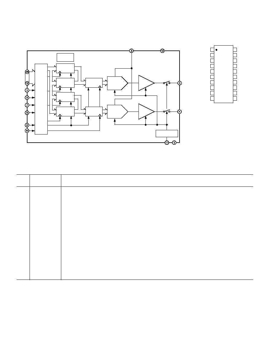
AD5342 FUNCTIONAL BLOCK DIAGRAM
V
OUT
A
BUFFER
AD5342
V
OUT
B
BUFFER
POWER-ON
RESET
DAC
REGISTER
DAC
REGISTER
INPUT
REGISTER
INPUT
REGISTER
INTER-
FACE
LOGIC
V
DD
DB
11
DB
0
CS
WR
A0
CLR
LDAC
.
.
.
V
REF
A
POWER-DOWN
LOGIC
RESET
PD GND
V
REF
B
12-BIT
DAC
12-BIT
DAC
AD5342 PIN FUNCTION DESCRIPTIONS
Pin
No.
Mnemonic
Function
1
GAIN
Gain Control Pin. This controls whether the output range from the DAC is 0-V
REF
or 0-2 V
REF
.
2
BUF
Buffer Control Pin. This pin controls whether the reference input to the DAC is buffered or unbuffered.
3
V
REF
B
Reference Input for DAC B.
4
V
REF
A
Reference Input for DAC A.
5
V
OUT
A
Output of DAC A. Buffered output with rail-to-rail operation.
6
V
OUT
B
Output of DAC B. Buffered output with rail-to-rail operation.
7, 8
NC
No Connect.
9
GND
Ground reference point for all circuitry on the part.
10
CS
Active Low Chip Select Input. This is used in conjunction with WR to write data to the parallel interface.
11
WR
Active low Write Input. This is used in conjunction with CS to write data to the parallel interface.
12
A0
Address pin for selecting between DAC A and DAC B.
13
CLR
Asynchronous active low control input that clears all input registers and DAC registers to zeros.
14
LDAC
Active low control input that updates the DAC registers with the contents of the input registers. This
allows all DAC outputs to be simultaneously updated.
15
PD
Power-Down Pin. This active low control pin puts all DACs into power-down mode.
16
V
DD
Power Supply Pin. These parts can operate from 2.5 V to 5.5 V and the supply should be decoupled with a
10 F capacitor in parallel with a 0.1 F capacitor to GND.
1728
DB
0
DB
11
12 Parallel Data Inputs. DB
11
is the MSB of these 12 bits.
AD5342 PIN CONFIGURATION
TOP VIEW
(Not to Scale)
28
27
26
25
24
23
22
21
20
19
18
17
16
15
1
2
3
4
5
6
7
8
9
10
11
12
13
14
AD5342
LDAC
A0
WR
CS
GND
BUF
V
REF
B
V
REF
A
V
OUT
B
V
OUT
A
GAIN
PD
V
DD
DB
0
DB
1
DB
2
DB
3
DB
4
DB
9
DB
8
DB
5
DB
6
DB
7
12-BIT
NC
NC
CLR
DB
10
DB
11
NC = NO CONNECT
REV. 0
AD5332/AD5333/AD5342/AD5343
8
AD5343 FUNCTIONAL BLOCK DIAGRAM
.
.
.
.
.
.
V
OUT
A
BUFFER
GND
AD5343
V
OUT
B
PD
LOW BYTE
REGISTER
V
DD
V
REF
HBEN
DB
7
DB
0
CS
WR
A0
CLR
LDAC
RESET
POWER-ON
RESET
HIGH BYTE
REGISTER
LOW BYTE
REGISTER
HIGH BYTE
REGISTER
POWER-DOWN
LOGIC
DAC
REGISTER
DAC
REGISTER
INTER-
FACE
LOGIC
BUFFER
12-BIT
DAC
12-BIT
DAC
AD5343 PIN FUNCTION DESCRIPTIONS
Pin
No.
Mnemonic
Function
1
HBEN
This pin is used when writing to the device to determine if data is written to the high byte register or the
low byte register.
2
V
REF
Unbuffered reference input for both DACs.
3
V
OUT
A
Output of DAC A. Buffered output with rail-to-rail operation.
4
V
OUT
B
Output of DAC B. Buffered output with rail-to-rail operation.
5
GND
Ground reference point for all circuitry on the part.
6
CS
Active Low Chip Select Input. This is used in conjunction with WR to write data to the parallel interface.
7
WR
Active Low Write Input. This is used in conjunction with CS to write data to the parallel interface.
8
A0
Address pin for selecting between DAC A and DAC B.
9
CLR
Asynchronous active low control input that clears all input registers and DAC registers to zeros.
10
LDAC
Active low control input that updates the DAC registers with the contents of the input registers. This allows
all DAC outputs to be simultaneously updated.
11
PD
Power-Down Pin. This active low control pin puts all DACs into power-down mode.
12
V
DD
Power Supply Pin. These parts can operate from 2.5 V to 5.5 V and the supply should be decoupled with a
10 F capacitor in parallel with a 0.1 F capacitor to GND.
1320
DB
0
DB
7
Eight Parallel Data Inputs. DB
7
is the MSB of these eight bits.
AD5343 PIN CONFIGURATION
TOP VIEW
(Not to Scale)
20
19
18
17
16
15
14
13
12
11
1
2
3
4
5
6
7
8
9
10
AD5343
LDAC
A0
WR
CS
GND
V
REF
V
OUT
B
V
OUT
A
PD
V
DD
DB
0
DB
1
DB
2
DB
3
DB
4
DB
5
DB
6
DB
7
12-BIT
CLR
HBEN
REV. 0
AD5332/AD5333/AD5342/AD5343
9
TERMINOLOGY
RELATIVE ACCURACY
For the DAC, Relative Accuracy or Integral Nonlinearity (INL)
is a measure of the maximum deviation, in LSBs, from a straight
line passing through the actual endpoints of the DAC transfer
function. Typical INL versus Code plot can be seen in Figures
5, 6, and 7.
DIFFERENTIAL NONLINEARITY
Differential Nonlinearity (DNL) is the difference between the
measured change and the ideal 1 LSB change between any two
adjacent codes. A specified differential nonlinearity of
±1 LSB
maximum ensures monotonicity. This DAC is guaranteed mono-
tonic by design. Typical DNL versus Code plot can be seen in
Figures 8, 9, and 10.
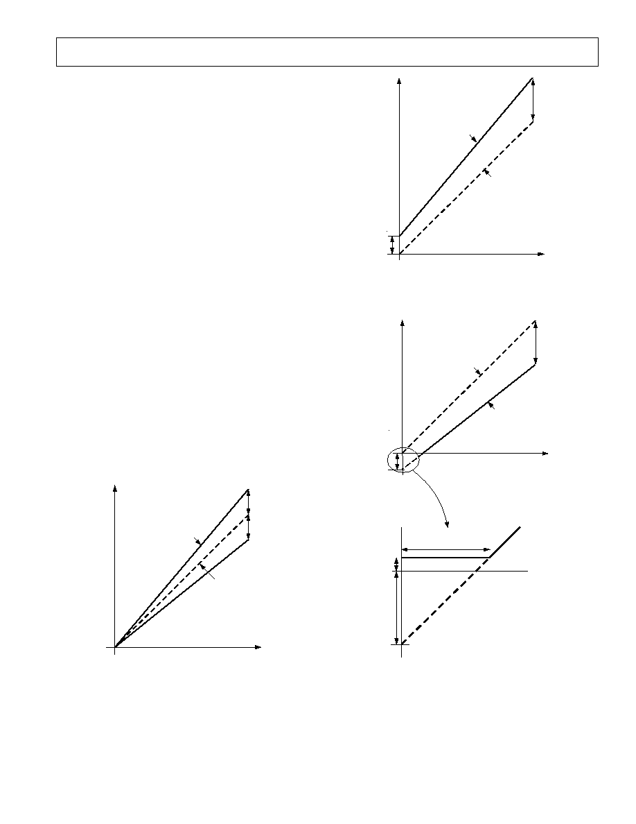
OFFSET ERROR
This is a measure of the offset error of the DAC and the output
amplifier. It is expressed as a percentage of the full-scale range.
If the offset voltage is positive, the output voltage will still be
positive at zero input code. This is shown in Figure 3. Because
the DACs operate from a single supply, a negative offset cannot
appear at the output of the buffer amplifier. Instead, there will
be a code close to zero at which the amplifier output saturates
(amplifier footroom). Below this code there will be a deadband
over which the output voltage will not change. This is illustrated
in Figure 4.
GAIN ERROR
This is a measure of the span error of the DAC (including any
error in the gain of the buffer amplifier). It is the deviation in
slope of the actual DAC transfer characteristic from the ideal
expressed as a percentage of the full-scale range. This is illus-
trated in Figure 2.
DAC CODE
POSITIVE
GAIN ERROR
NEGATIVE
GAIN ERROR
OUTPUT
VOLTAGE
ACTUAL
IDEAL
Figure 2. Gain Error
DAC CODE
POSITIVE
OFFSET
OUTPUT
VOLTAGE
GAIN ERROR
AND
OFFSET
ERROR
ACTUAL
IDEAL
Figure 3. Positive Offset Error and Gain Error
OUTPUT
VOLTAGE
DAC CODE
NEGATIVE
OFFSET
GAIN ERROR
AND
OFFSET
ERROR
AMPLIFIER
FOOTROOM
(~ 1mV)
NEGATIVE
OFFSET
DEADBAND CODES
ACTUAL
IDEAL
Figure 4. Negative Offset Error and Gain Error

REV. 0
AD5332/AD5333/AD5342/AD5343
10
OFFSET ERROR DRIFT
This is a measure of the change in Offset Error with changes in
temperature. It is expressed in (ppm of full-scale range)/
°C.
GAIN ERROR DRIFT
This is a measure of the change in Gain Error with changes in tem-
perature. It is expressed in (ppm of full-scale range)/
°C.
POWER-SUPPLY REJECTION RATIO (PSRR)
This indicates how the output of the DAC is affected by changes in
the supply voltage. PSRR is the ratio of the change in V
OUT
to a
change in V
DD
for full-scale output of the DAC. It is measured
in dBs. V
REF
is held at 2 V and V
DD
is varied
±10%.
DC CROSSTALK
This is the dc change in the output level of one DAC at mid-
scale in response to a full-scale code change (all 0s to all 1s and
vice versa) and output change of the other DAC. It is expressed
in
µV.
REFERENCE FEEDTHROUGH
This is the ratio of the amplitude of the signal at the DAC output
to the reference input when the DAC output is not being updated
(i.e., LDAC is high). It is expressed in dBs.
CHANNEL-TO-CHANNEL ISOLATION
This is a ratio of the amplitude of the signal at the output of one
DAC to a sine wave on the reference input of the other DAC. It
is measured by grounding one V
REF
pin and applying a 10 kHz,
4 V peak-to-peak sine wave to the other V
REF
pin. It is expressed
in dBs.
MAJOR-CODE TRANSITION GLITCH ENERGY
Major-Code Transition Glitch Energy is the energy of the
impulse injected into the analog output when the DAC changes
state. It is normally specified as the area of the glitch in nV secs
and is measured when the digital code is changed by 1 LSB at
the major carry transition (011 . . . 11 to 100 . . . 00 or 100 . . . 00
to 011 . . . 11).
DIGITAL FEEDTHROUGH
Digital Feedthrough is a measure of the impulse injected into
the analog output of the DAC from the digital input pins of the
device but is measured when the DAC is not being written to
(CS held high). It is specified in nV secs and is measured with a
full-scale change on the digital input pins, i.e. from all 0s to all
1s and vice versa.
DIGITAL CROSSTALK
This is the glitch impulse transferred to the output of one DAC
at midscale in response to a full-scale code change (all 0s to all
1s and vice versa) in the input register of the other DAC. It is
expressed in nV-secs.
ANALOG CROSSTALK
This is the glitch impulse transferred to the output of one DAC
due to a change in the output of the other DAC. It is measured
by loading one of the input registers with a full-scale code change
(all 0s to all 1s and vice versa) while keeping LDAC high. Then
pulse LDAC low and monitor the output of the DAC whose
digital code was not changed. The area of the glitch is expressed
in nV-secs.
DAC-TO-DAC CROSSTALK
This is the glitch impulse transferred to the output of one DAC
due to a digital code change and subsequent output change of
the other DAC. This includes both digital and analog crosstalk.
It is measured by loading one of the DACs with a full-scale code
change (all 0s to all 1s and vice versa) with the LDAC pin set
low and monitoring the output of the other DAC. The energy of
the glitch is expressed in nV-secs.
MULTIPLYING BANDWIDTH
The amplifiers within the DAC have a finite bandwidth. The
Multiplying Bandwidth is a measure of this. A sine wave on the
reference (with full-scale code loaded to the DAC) appears on
the output. The Multiplying Bandwidth is the frequency at which
the output amplitude falls to 3 dB below the input.
TOTAL HARMONIC DISTORTION
This is the difference between an ideal sine wave and its attenuated
version using the DAC. The sine wave is used as the reference
for the DAC and the THD is a measure of the harmonics present
on the DAC output. It is measured in dBs.
REV. 0
AD5332/AD5333/AD5342/AD5343
11
Typical Performance Characteristics
CODE
INL ERROR LSBs
1.0
0.5
1.0
0
50
250
100
150
200
0
0.5
T
A
= 25 C
V
DD
= 5V
Figure 5. AD5332 Typical INL Plot
CODE
DNL ERROR
LSBs
0
50
250
100
150
200
0.1
0.2
0.3
0.3
0.1
0.2
0
T
A
= 25 C
V
DD
= 5V
Figure 8. AD5332 Typical DNL Plot
V
REF
V
1.00
1.00
0.25
0.00
0.75
0.50
ERROR
LSBs
2
3
4
5
0.25
0.50
0.75
V
DD
= 5V
T
A
= 25 C
MAX INL
MAX DNL
MIN DNL
MIN INL
Figure 11. AD5332 INL and DNL
Error vs. V
REF
CODE
INL ERROR
LSBs
3
0
200
1000
400
600
800
0
1
2
3
2
1
T
A
= 25 C
V
DD
= 5V
Figure 6. AD5333 Typical INL Plot
CODE
DNL ERROR
LSBs
0.4
0.4
600
400
800
1000
0
0.6
0.6
0.2
0.2
T
A
= 25 C
V
DD
= 5V
200
0
Figure 9. AD5333 Typical DNL Plot
TEMPERATURE C
ERROR
LSBs
1.00
0.75
1.00
40
0
120
40
80
0
0.25
0.50
0.75
0.50
0.25
V
DD
= 5V
V
REF
= 2V
MAX INL
MAX DNL
MIN DNL
MIN INL
Figure 12. AD5332 INL Error and
DNL Error vs. Temperature
CODE
INL ERROR
LSBs
12
0
4
8
8
4
0
4000
1000
2000
3000
12
T
A
= 25 C
V
DD
= 5V
Figure 7. AD5342 Typical INL Plot
CODE
DNL ERROR
LSBs
1.0
0.5
1
0
1000
4000
2000
3000
0
0.5
T
A
= 25 C
V
DD
= 5V
Figure 10. AD5342 Typical DNL Plot
TEMPERATURE C
ERROR
%
40
0
120
40
80
0.0
0.5
1.0
1.0
0.5
V
DD
= 5V
V
REF
= 2V
GAIN ERROR
OFFSET ERROR
Figure 13. AD5332 Offset Error
and Gain Error vs. Temperature
REV. 0
AD5332/AD5333/AD5342/AD5343
12
GAIN ERROR
V
DD
Volts
ERROR
%
0.2
0.6
0
1
3
0
0.4
T
A
= 25 C
V
REF
= 2V
4
6
0.5
0.3
0.2
0.1
0.1
2
5
OFFSET ERROR
Figure 14. Offset Error and Gain
Error vs. V
DD
400
100
0
2.5
5.5
3.0
3.5
4.0
4.5
5.0
V
DD
V
I
DD
A
200
300
T
A
= 25 C
Figure 17. Supply Current vs. Supply
Voltage
CH1 1V, CH2 5V, TIME BASE = 5 s/DIV
CH2
CH1
LDAC
V
OUT
V
DD
= 5V
T
A
= 25 C
Figure 20. Half-Scale Settling (1/4 to
3/4 Scale Code Change)
5V SOURCE
SINK/SOURCE CURRENT mA
V
OUT
Volts
5
0
0
1
3
4
4
6
1
2
3
2
5
3V SOURCE
3V SINK
5V SINK
Figure 15. V
OUT
Source and Sink
Current Capability
0.5
0.1
0
2.5
5.5
3.0
3.5
4.0
4.5
5.0
V
DD
V
I
DD
A
0.2
0.3
0.4
T
A
= 25 C
Figure 18. Power-Down Current vs.
Supply Voltage
V
DD
CH1
CH2
V
OUT
A
T
A
= 25 C
V
DD
= 5V
V
REF
= 2V
CH1 2V, CH2 200mV, TIME BASE = 200 s/DIV
Figure 21. Power-On Reset to 0 V
DAC CODE
400
50
0
ZERO-SCALE
FULL-SCALE
I
DD
A
100
150
200
250
300
350
V
DD
= 3.6V
V
DD
= 5.5V
T
A
= 25 C
V
REF
= 2V
Figure 16. Supply Current vs. DAC
Code
V
LOGIC
V
1600
800
0
0
1
2
3
4
5
I
DD
A
200
400
600
1000
1200
1400
T
A
= 25 C
V
DD
= 5V
V
DD
= 3V
Figure 19. Supply Current vs. Logic
Input Voltage
CH1 500mV, CH2 5V, TIME BASE = 1 s/DIV
CH1
CH2
T
A
= 25 C
V
DD
= 5V
V
REF
= 2V
V
OUT
A
PD
Figure 22. Exiting Power-Down to
Midscale
REV. 0
AD5332/AD5333/AD5342/AD5343
13
I
DD
A
FREQUENCY
0
100
150
400
200
250
350
300
V
DD
= +5V
V
DD
= +3V
Figure 23. I
DD
Histogram with V
DD
= 3
V and V
DD
= 5 V
0.4
0
6
1
2
3
4
5
V
REF
V
FULL-SCALE ERROR
%FSR
0.2
0
0.2
T
A
= 25 C
V
REF
= 2V
Figure 26. Full-Scale Error vs. V
REF
500 ns/DIV
0.939
0.938
0.937
0.936
0.935
0.934
0.933
0.932
0.931
0.930
0.929
V
OUT
Volts
Figure 24. AD5342 Major-Code Tran-
sition Glitch Energy
4mV/DIV
750ns/DIV
Figure 27. DAC-DAC Crosstalk
FREQUENCY kHz
10
40
0.01
20
30
0
10
dB
0.1
1
10
100
1k
10k
50
60
Figure 25. Multiplying Bandwidth
(Small-Signal Frequency Response)
FUNCTIONAL DESCRIPTION
The AD5332/AD5333/AD5342/AD5343 are dual DACs fabri-
cated on a CMOS process with resolutions of 8, 10, 12, and
12 bits, respectively. They are written to using a parallel inter-
face. They operate from single supplies of 2.5 V to 5.5 V and
the output buffer amplifiers offer rail-to-rail output swing. The
AD5333 and AD5342 have reference inputs that may be buff-
ered to draw virtually no current from the reference source.
Their output voltage range may be configured to be 0 to V
REF
or 0 to 2 V
REF
. The reference inputs of the AD5332 and AD5343
are unbuffered and their output range is 0 to V
REF
. The devices
have a power-down feature that reduces current consumption to
only 80 nA @ 3 V.
Digital-to-Analog Section
The architecture of one DAC channel consists of a reference
buffer and a resistor-string DAC followed by an output buffer
amplifier. The voltage at the V
REF
pin provides the reference
voltage for the DAC. Figure 28 shows a block diagram of the
DAC architecture. Since the input coding to the DAC is straight
binary, the ideal output voltage is given by:
V
V
D
Gain
OUT
REF
N
=
×
×
2
where:
D = decimal equivalent of the binary code which is loaded to
the DAC register:
0255 for AD5332 (8 Bits)
01023 for AD5333 (10 Bits)
04095 for AD5342/AD5343 (12 Bits)
N = DAC resolution
Gain = Output Amplifier Gain (1 or 2)
V
OUT
GAIN
V
REF
BUF
DAC
REGISTER
INPUT
REGISTER
RESISTOR
STRING
OUTPUT
BUFFER AMPLIFIER
REFERENCE
BUFFER
Figure 28. Single DAC Channel Architecture
REV. 0
AD5332/AD5333/AD5342/AD5343
14
PARALLEL INTERFACE
The AD5332, AD5333, and AD5342 load their data as a single
8-, 10-, or 12-bit word, while the AD5343 loads data as a low
byte of 8 bits and a high byte containing 4 bits.
Double-Buffered Interface
The AD5332/AD5333/AD5342/AD5343 DACs all have double-
buffered interfaces consisting of an input register and a DAC
register. DAC data, BUF, and GAIN inputs are written to the
input register under control of the Chip Select (CS) and Write
(WR).
Access to the DAC register is controlled by the LDAC function.
When LDAC is high, the DAC register is latched and the input
register may change state without affecting the contents of the
DAC register. However, when LDAC is brought low, the DAC
register becomes transparent and the contents of the input
register are transferred to it. The gain and buffer control signals
are also double-buffered and are only updated when LDAC is
taken low.
This is useful if the user requires simultaneous updating of all
DACs and peripherals. The user may write to both input regis-
ters individually and then, by pulsing the LDAC input low, both
outputs will update simultaneously.
Double-buffering is also useful where the DAC data is loaded in
two bytes, as in the AD5343, because it allows the whole data
word to be assembled in parallel before updating the DAC register.
This prevents spurious outputs that could occur if the DAC
register were updated with only the high byte or the low byte.
These parts contain an extra feature whereby the DAC register
is not updated unless its input register has been updated since
the last time that LDAC was brought low. Normally, when
LDAC is brought low, the DAC registers are filled with the
contents of the input registers. In the case of the AD5332/
AD5333/AD5342/AD5343, the part will only update the DAC
register if the input register has been changed since the last
time the DAC register was updated. This removes unnecessary
crosstalk.
Clear Input (CLR)
CLR is an active low, asynchronous clear that resets the input and
DAC registers.
Chip Select Input (CS)
CS is an active low input that selects the device.
Write Input (WR)
WR is an active low input that controls writing of data to the
device. Data is latched into the input register on the rising edge
of WR.
Load DAC Input (LDAC)
LDAC transfers data from the input register to the DAC register
(and hence updates the outputs). Use of the LDAC function enables
double buffering of the DAC data, GAIN and BUF. There are
two LDAC modes:
Synchronous Mode: In this mode the DAC register is updated
after new data is read in on the rising edge of the WR input.
LDAC can be tied permanently low or pulsed as in Figure 1.
Asynchronous Mode: In this mode the outputs are not updated
at the same time that the input register is written to. When LDAC
goes low the DAC register is updated with the contents of the
input register.
Resistor String
The resistor string section is shown in Figure 29. It is simply a
string of resistors, each of value R. The digital code loaded to
the DAC register determines at what node on the string the
voltage is tapped off to be fed into the output amplifier. The
voltage is tapped off by closing one of the switches connecting
the string to the amplifier. Because it is a string of resistors, it
is guaranteed monotonic.
TO OUTPUT
AMPLIFIER
R
R
R
R
R
V
REF
Figure 29. Resistor String
DAC Reference Input
The DACs operate with an external reference. The AD5332,
AD5333, and AD5342 have separate reference inputs for each
DAC, while the AD5343 has a single reference input for both
DACs. The reference inputs on the AD5333 and AD5342 may
be configured as buffered or unbuffered. The reference inputs
of the AD5332 and AD5343 are unbuffered. The buffered/
unbuffered option is controlled by the BUF pin.
In buffered mode (BUF = 1) the current drawn from an exter-
nal reference voltage is virtually zero, as the impedance is at
least 10 M
. The reference input range is 1 V to V
DD
.
In unbuffered mode (BUF = 0) the user can have a reference
voltage as low as 0.25 V and as high as V
DD
since there is no
restriction due to headroom and footroom of the reference ampli-
fier. The impedance is still large at typically 180 k
for 0V
REF
mode and 90 k
for 02 V
REF
mode.
If using an external buffered reference (e.g., REF192) there is
no need to use the on-chip buffer.
Output Amplifier
The output buffer amplifier is capable of generating output volt-
ages to within 1 mV of either rail. Its actual range depends on
V
REF
, GAIN, the load on V
OUT
and offset error.
If a gain of 1 is selected (GAIN = 0), the output range is 0.001 V
to V
REF
.
If a gain of 2 is selected (GAIN = 1), on the AD5333 and AD5342
the output range is 0.001 V to 2 V
REF
.
The output amplifier is capable of driving a load of 2 k
to
GND or V
DD
, in parallel with 500 pF to GND or V
DD
. The
source and sink capabilities of the output amplifier can be seen
in Figure 15.
The slew rate is 0.7 V/
µs with a half-scale settling time to ±0.5 LSB
(at 8 bits) of 6
µs with the output unloaded. See Figure 20.
REV. 0
AD5332/AD5333/AD5342/AD5343
15
High-Byte Enable Input (HBEN)
High-Byte Enable is a control input on the AD5343 only that
determines if data is written to the high-byte input register or
the low-byte input register.
The low data byte of the AD5343 consists of data bits 0 to 7 at
data inputs DB
0
to DB
7
, while the high byte consists of data
bits 8 to 11 at data inputs DB
0
to DB
3
. DB
4
to DB
7
are ignored
during a high byte write, but they may be used for data to
set up the reference input as buffered/unbuffered, and buffer
amplifier gain. See Figure 32.
DB8
DB9
X
X
HIGH BYTE
LOW BYTE
X = UNUSED BIT
DB0
DB1
DB2
DB3
DB4
DB5
DB6
DB7
X
X
DB10
DB11
Figure 30. Data Format for AD5343
POWER-ON RESET
The AD5332/AD5333/AD5342/AD5343 are provided with a
power-on reset function, so that they power up in a defined state.
The power-on state is:
· Normal operation
· Reference input unbuffered
· 0 V
REF
output range
· Output voltage set to 0 V
Both input and DAC registers are filled with zeros and remain
so until a valid write sequence is made to the device. This is
particularly useful in applications where it is important to know
the state of the DAC outputs while the device is powering up.
POWER-DOWN MODE
The AD5332/AD5333/AD5342/AD5343 have low power con-
sumption, dissipating typically 0.69 mW with a 3 V supply and
1.5 mW with a 5 V supply. Power consumption can be further
reduced when the DACs are not in use by putting them into
power-down mode, which is selected by taking pin PD low.
When the PD pin is high, the DACs work normally with a typical
power consumption of 300
µA at 5 V (230 µA at 3 V). In power-
down mode, however, the supply current falls to 200 nA at 5 V
(80 nA at 3 V) when both DACs are powered down. Not only
does the supply current drop, but the output stage is also internally
switched from the output of the amplifier, making it open-circuit.
This has the advantage that the outputs are three-state while
the part is in power-down mode, and provides a defined input
condition for whatever is connected to the outputs of the DAC
amplifiers. The output stage is illustrated in Figure 31.
RESISTOR
STRING DAC
POWER-DOWN
CIRCUITRY
AMPLIFIER
VOUT
Figure 31. Output Stage During Power-Down
The bias generator, the output amplifier, the resistor string, and
all other associated linear circuitry are all shut down when the
power-down mode is activated. However, the contents of the
registers are unaffected when in power-down. The time to exit
power-down is typically 2.5
µs for V
DD
= 5 V and 5
µs when
V
DD
= 3 V. This is the time from a rising edge on the PD pin to
when the output voltage deviates from its power-down voltage.
See Figure 22.
Table I. AD5332/AD5333/AD5342 Truth Table
CLR
LDAC
CS
WR
A0
Function
1
1
1
X
X
No Data Transfer
1
1
X
1
X
No Data Transfer
0
X
X
X
X
Clear All Registers
1
1
0
0
1
0
Load DAC A Input Register
1
1
0
0
1
1
Load DAC B Input Register
1
0
X
X
X
Update DAC Registers
X = don't care.
Table II. AD5343 Truth Table
CLR
LDAC
CS
WR
A0
HBEN
Function
1
1
1
X
X
X
No Data Transfer
1
1
X
1
X
X
No Data Transfer
0
X
X
X
X
X
Clear All Registers
1
1
0
0
1
0
0
Load DAC A Low Byte Input Register
1
1
0
0
1
0
1
Load DAC A High Byte Input Register
1
1
0
0
1
1
0
Load DAC B Low Byte Input Register
1
1
0
0
1
1
1
Load DAC B High Byte Input Register
1
0
X
X
X
X
Update DAC Registers
X = don't care.
REV. 0
AD5332/AD5333/AD5342/AD5343
16
SUGGESTED DATABUS FORMATS
In most applications GAIN and BUF are hard-wired. However,
if more flexibility is required, they can be included in a databus.
This enables you to software program GAIN, giving the option
of doubling the resolution in the lower half of the DAC range.
In a bused system GAIN and BUF may be treated as data inputs
since they are written to the device during a write operation and
take effect when LDAC is taken low. This means that the refer-
ence buffers and the output amplifier gain of multiple DAC
devices can be controlled using common GAIN and BUF lines.
The AD5333 and AD5342 databuses must be at least 10, and
12 bits wide respectively, and are best suited to a 16-bit data-
bus system.
Examples of data formats for putting GAIN and BUF on a 16-
bit databus are shown in Figure 32. Note that any unused bits
above the actual DAC data may be used for BUF and GAIN.
DB0
DB1
DB2
DB3
DB4
DB5
DB6
DB7
DB8
DB9
GAIN
X
X
AD5342
X = UNUSED BIT
BUF
DB0
DB1
DB2
DB3
DB4
DB5
DB6
DB7
DB8
DB9
GAIN
X
X
AD5333
X
X
BUF
DB10
DB11
Figure 32. GAIN and BUF Data on a 16-Bit Bus
APPLICATIONS INFORMATION
Typical Application Circuits
The AD5332/AD5333/AD5342/AD5343 can be used with a
wide range of reference voltages, especially if the reference inputs
are configured to be unbuffered, in which case the devices offer
full, one-quadrant multiplying capability over a reference range
of 0.25 V to V
DD
. More typically, these devices may be used with a
fixed, precision reference voltage. Figure 33 shows a typical
setup for the devices when using an external reference connected to
the unbuffered reference inputs. If the reference inputs are unbuf-
fered, the reference input range is from 0.25 V to V
DD
, but if the
on-chip reference buffers are used, the reference range is reduced.
Suitable references for 5 V operation are the AD780 and REF192.
For 2.5 V operation, a suitable external reference would be the
AD589, a 1.23 V bandgap reference.
AD5332/AD5333/
AD5342/AD5343
V
OUT
*
0.1 F
V
DD
= 2.5V TO 5.5V
V
DD
GND
AD780/REF192
WITH V
DD
= 5V
OR
AD589 WITH V
DD
= 2.5V
V
REF
*
GND
V
OUT
V
IN
EXT
REF
*ONLY ONE CHANNEL OF V
REF
AND V
OUT
SHOWN
10 F
Figure 33. AD5332/AD5333/AD5342/AD5343 Using
External Reference
Driving V
DD
from the Reference Voltage
If an output range of zero to V
DD
is required when the reference
inputs are configured as unbuffered, the simplest solution is to
connect the reference inputs to V
DD
. As this supply may not be
very accurate, and may be noisy, the devices may be powered
from the reference voltage, for example using a 5 V reference
such as the ADM663 or ADM666, as shown in Figure 34.
AD5332/AD5333/
AD5342/AD5343
V
OUT
*
V
DD
GND
V
REF
*
GND
V
OUT(2)
V
IN
ADM663/ADM666
VSET
SHDN
SENSE
6V TO 16V
*ONLY ONE CHANNEL OF V
REF
AND V
OUT
SHOWN
0.1 F
10 F
0.1 F
Figure 34. Using an ADM663/ADM666 as Power and Refer-
ence to AD5332/AD5333/AD5342/AD5343
Bipolar Operation Using the AD5332/AD5333/AD5342/AD5343
The AD5332/AD5333/AD5342/AD5343 have been designed
for single supply operation, but bipolar operation is achievable
using the circuit shown in Figure 35. The circuit shown has been
configured to achieve an output voltage range of 5 V < V
O
<
+5 V. Rail-to-rail operation at the amplifier output is achievable
using an AD820 or OP295 as the output amplifier.
The output voltage for any input code can be calculated as
follows:
V
O
= [(1 + R4/R3)
× (R2/(R1 + R2) × (2 × V
REF
× D/2
N
)] R4
× V
REF
/R3
where:
D is the decimal equivalent of the code loaded to the DAC, N is
DAC resolution and V
REF
is the reference voltage input.
With:
V
REF
= 2.5 V
R1 = R3 = 10 k
R2 = R4 = 20 k
and V
DD
= 5 V.
V
OUT
= (10
× D/2
N
) 5
AD5332/AD5333/
AD5342/AD5343
GND
V
DD
= 5V
EXT
REF
V
OUT
*
AD780/REF192
WITH V
DD
= 5V
OR
AD589 WITH V
DD
= 2.5V
GND
V
IN
V
OUT
V
REF
*
V
DD
R3
10k
R1
10k
R2
20k
R4
20k
5V
+5V
5V
*ONLY ONE CHANNEL OF V
REF
AND V
OUT
SHOWN
0.1 F
0.1 F
10 F
Figure 35. Bipolar Operation using the AD5332/AD5333/
AD5342/AD5343
REV. 0
AD5332/AD5333/AD5342/AD5343
17
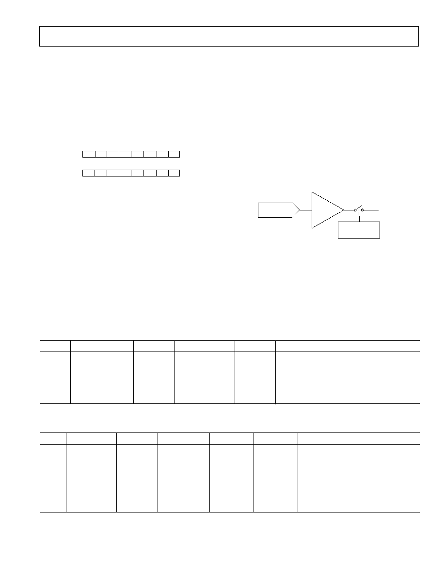
Decoding Multiple AD5332/AD5333/AD5342/AD5343
The CS pin on these devices can be used in applications to decode
a number of DACs. In this application, all DACs in the system
receive the same data and WR pulses, but only the CS to one of
the DACs will be active at any one time, so data will only be
written to the DAC whose CS is low. If multiple AD5343s are
being used, a common HBEN line will also be required to
determine if the data is written to the high-byte or low-byte
register of the selected DAC.
The 74HC139 is used as a 2- to 4-line decoder to address any
of the DACs in the system. To prevent timing errors from
occurring, the enable input should be brought to its inactive
state while the coded address inputs are changing state. Figure 36
shows a diagram of a typical setup for decoding multiple devices
in a system. Once data has been written sequentially to all DACs in
a system, all the DACs can be updated simultaneously using a
common LDAC line. A common CLR line can also be used to
reset all DAC outputs to zero.
ENABLE
CODED
ADDRESS
1G
1A
1B
V
DD
V
CC
74HC139
DGND
1Y0
1Y1
1Y2
1Y3
A1
HBEN
WR
LDAC
CLR
DATA
INPUTS
DATA
INPUTS
DATA
INPUTS
DATA
INPUTS
DATA BUS
*AD5343 ONLY
A0
HBEN*
WR
LDAC
CLR
CS
AD5332/AD5333/
AD5342/AD5343
AD5332/AD5333/
AD5342/AD5343
AD5332/AD5333/
AD5342/AD5343
AD5332/AD5333/
AD5342/AD5343
A0
HBEN*
WR
LDAC
CLR
CS
A0
HBEN*
WR
LDAC
CLR
CS
A0
HBEN*
WR
LDAC
CLR
CS
Figure 36. Decoding Multiple DAC Devices
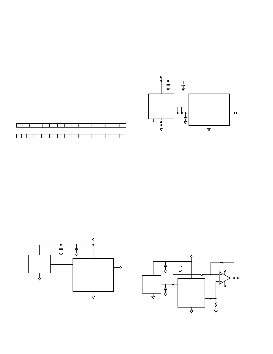
AD5332/AD5333/AD5342/AD5343 as a Digitally Program-
mable Window Detector
A digitally programmable upper/lower limit detector using the
two DACs in the AD5332/AD5333/AD5342 is shown in Figure
37. The upper and lower limits for the test are loaded to DACs
A and B which, in turn, set the limits on the CMP04. If a signal
at the V
IN
input is not within the programmed window, an LED
will indicate the fail condition.
Note that the AD5343 has only a single reference input. If using
the AD5332, AD5333, or AD5342, both reference inputs must
be connected.
5V
0.1 F
10 F
AD5332/AD5333/
AD5342
GND
V
DD
V
OUT
V
REF
B*
*NOT AD5343
V
OUT
B
V
IN
FAIL
PASS
1k
1k
PASS/
FAIL
1/6 74HC05
1/2
CMP04
V
REF
A*
V
REF
Figure 37. Programmable Window Detector
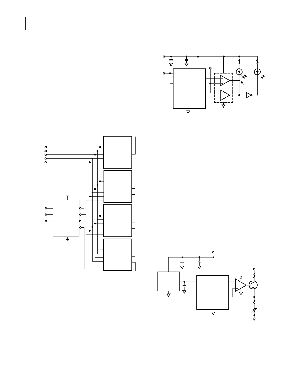
Programmable Current Source
Figure 38 shows the AD5332/AD5333/AD5342/AD5343 used
as the control element of a programmable current source. In this
example, the full-scale current is set to 1 mA. The output volt-
age from the DAC is applied across the current setting resistor
of 4.7 k
in series with the 470 adjustment potentiometer,
which gives an adjustment of about
±5%. Suitable transistors to
place in the feedback loop of the amplifier include the BC107
and the 2N3904, which enable the current source to operate
from a minimum V
SOURCE
of 6 V. The operating range is deter-
mined by the operating characteristics of the transistor. Suitable
amplifiers include the AD820 and the OP295, both having rail-
to-rail operation on their outputs. The current for any digital
input code and resistor value can be calculated as follows:
I
G
V
D
R
mA
REF
N
=
×
×
×
(
)
2
Where:
G is the gain of the buffer amplifier (1 or 2)
D is the digital equivalent of the digital input code
N is the DAC resolution (8, 10, or 12 bits)
R is the sum of the resistor plus adjustment potentiometer in k
AD5332/AD5333/
AD5342/AD5343
GND
V
DD
= 5V
EXT
REF
V
OUT
*
AD780/REF192
WITH V
DD
= 5V
GND
V
IN
V
OUT
V
REF
*
V
DD
4.7k
5V
*ONLY ONE CHANNEL OF V
REF
AND V
OUT
SHOWN
0.1 F
0.1 F
10 F
470
LOAD
V
SOURCE
Figure 38. Programmable Current Source
REV. 0
AD5332/AD5333/AD5342/AD5343
18
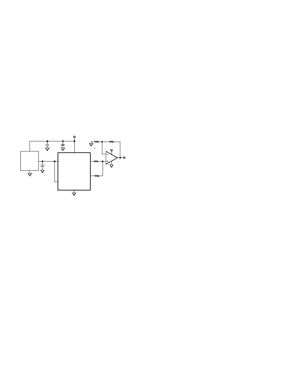
Coarse and Fine Adjustment Using the AD5332/AD5333/
AD5342/AD5343
The DACs in the AD5332/AD5333/AD5342/AD5343 can be
paired together to form a coarse and fine adjustment function,
as shown in Figure 39. DAC A is used to provide the coarse
adjustment while DAC B provides the fine adjustment. Varying
the ratio of R1 and R2 will change the relative effect of the coarse
and fine adjustments. With the resistor values shown the output
amplifier has unity gain for the DAC A output, so the output
range is 0 V to 2.5 V 1 LSB. For DAC B the amplifier has a gain
of 7.6
× 10
3
, giving DAC B a range equal to 2 LSBs of DAC A.
The circuit is shown with a 2.5 V reference, but reference volt-
ages up to V
DD
may be used. The op amps indicated will allow a
rail-to-rail output swing.
Note that the AD5343 has only a single reference input. If using
the AD5332, AD5333, or AD5342, both reference inputs must
be connected.
GND
V
DD
= 5V
EXT
REF
AD780/REF192
WITH V
DD
= 5V
V
IN
V
OUT
R2
51.2k
V
OUT
+5V
0.1 F
0.1 F
10 F
AD5332/AD5333/
AD5342/AD5343
GND
V
REF
A*
V
DD
V
OUT
A
R1
390
V
REF
B*
*NOT AD5343
V
OUT
B
R4
390
R3
51.2k
Figure 39. Coarse and Fine Adjustment
Power Supply Bypassing and Grounding
In any circuit where accuracy is important, careful consideration
of the power supply and ground return layout helps to ensure
the rated performance. The printed circuit board on which the
AD5332/AD5333/AD5342/AD5343 is mounted should be
designed so that the analog and digital sections are separated,
and confined to certain areas of the board. If the device is in a
system where multiple devices require an AGND-to-DGND
connection, the connection should be made at one point only.
The star ground point should be established as closely as pos-
sible to the device. The AD5332/AD5333/AD5342/AD5343
should have ample supply bypassing of 10
µF in parallel with
0.1
µF on the supply located as close to the package as pos-
sible, ideally right up against the device. The 10
µF capacitors
are the tantalum bead type. The 0.1
µF capacitor should have
low Effective Series Resistance (ESR) and Effective Series Induc-
tance (ESI), like the common ceramic types that provide a low
impedance path to ground at high frequencies to handle tran-
sient currents due to internal logic switching.
The power supply lines of the device should use as large a trace
as possible to provide low impedance paths and reduce the effects
of glitches on the power supply line. Fast switching signals such
as clocks should be shielded with digital ground to avoid radiat-
ing noise to other parts of the board, and should never be run
near the reference inputs. Avoid crossover of digital and ana-
log signals. Traces on opposite sides of the board should run
at right angles to each other. This reduces the effects of feed-
through through the board. A microstrip technique is by far
the best, but not always possible with a double-sided board. In
this technique, the component side of the board is dedicated to
ground plane while signal traces are placed on the solder side.

REV. 0
AD5332/AD5333/AD5342/AD5343
19
Table III. Overview of AD53xx Parallel Devices
Part No.
Resolution DNL
V
REF
Pins
Settling Time
Additional Pin Functions
Package
Pins
SINGLES
BUF
GAIN
HBEN
CLR
AD5330
8
±0.25
1
6
µs
TSSOP
20
AD5331
10
±0.5
1
7
µs
TSSOP
20
AD5340
12
±1.0
1
8
µs
TSSOP
24
AD5341
12
±1.0
1
8
µs
TSSOP
20
DUALS
AD5332
8
±0.25
2
6
µs
TSSOP
20
AD5333
10
±0.5
2
7
µs
TSSOP
24
AD5342
12
±1.0
2
8
µs
TSSOP
28
AD5343
12
±1.0
1
8
µs
TSSOP
20
QUADS
AD5334
8
±0.25
2
6
µs
TSSOP
24
AD5335
10
±0.5
2
7
µs
TSSOP
24
AD5336
10
±0.5
4
7
µs
TSSOP
28
AD5344
12
±1.0
4
8
µs
TSSOP
28
Table IV. Overview of AD53xx Serial Devices
Part No.
Resolution
No. of DACS
DNL
Interface
Settling Time
Package
Pins
SINGLES
AD5300
8
1
±0.25
SPI
4
µs
SOT-23, MicroSOIC
6, 8
AD5310
10
1
±0.5
SPI
6
µs
SOT-23, MicroSOIC
6, 8
AD5320
12
1
±1.0
SPI
8
µs
SOT-23, MicroSOIC
6, 8
AD5301
8
1
±0.25
2-Wire
6
µs
SOT-23, MicroSOIC
6, 8
AD5311
10
1
±0.5
2-Wire
7
µs
SOT-23, MicroSOIC
6, 8
AD5321
12
1
±1.0
2-Wire
8
µs
SOT-23, MicroSOIC
6, 8
DUALS
AD5302
8
2
±0.25
SPI
6
µs
MicroSOIC
8
AD5312
10
2
±0.5
SPI
7
µs
MicroSOIC
8
AD5322
12
2
±1.0
SPI
8
µs
MicroSOIC
8
AD5303
8
2
±0.25
SPI
6
µs
TSSOP
16
AD5313
10
2
±0.5
SPI
7
µs
TSSOP
16
AD5323
12
2
±1.0
SPI
8
µs
TSSOP
16
QUADS
AD5304
8
4
±0.25
SPI
6
µs
MicroSOIC
10
AD5314
10
4
±0.5
SPI
7
µs
MicroSOIC
10
AD5324
12
4
±1.0
SPI
8
µs
MicroSOIC
10
AD5305
8
4
±0.25
2-Wire
6
µs
MicroSOIC
10
AD5315
10
4
±0.5
2-Wire
7
µs
MicroSOIC
10
AD5325
12
4
±1.0
2-Wire
8
µs
MicroSOIC
10
AD5306
8
4
±0.25
2-Wire
6
µs
TSSOP
16
AD5316
10
4
±0.5
2-Wire
7
µs
TSSOP
16
AD5326
12
4
±1.0
2-Wire
8
µs
TSSOP
16
AD5307
8
4
±0.25
SPI
6
µs
TSSOP
16
AD5317
10
4
±0.5
SPI
7
µs
TSSOP
16
AD5327
12
4
±1.0
SPI
8
µs
TSSOP
16
Visit our web-page at http://www.analog.com/support/standard_linear/selection_guides/AD53xx.html
REV. 0
20
C3829
2.5
4/00 (rev. 0)
PRINTED IN U.S.A.
AD5332/AD5333/AD5342/AD5343
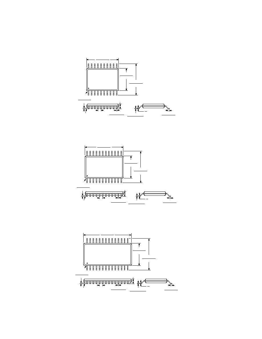
OUTLINE DIMENSIONS
Dimensions shown in inches and (mm).
20-Lead Thin Shrink Small Outline Package TSSOP
(RU-20)
20
11
10
1
0.256 (6.50)
0.246 (6.25)
0.177 (4.50)
0.169 (4.30)
PIN 1
0.260 (6.60)
0.252 (6.40)
SEATING
PLANE
0.006 (0.15)
0.002 (0.05)
0.0118 (0.30)
0.0075 (0.19)
0.0256 (0.65)
BSC
0.0433 (1.10)
MAX
0.0079 (0.20)
0.0035 (0.090)
0.028 (0.70)
0.020 (0.50)
8
0
24-Lead Thin Shrink Small Outline Package TSSOP
(RU-24)
24
13
12
1
0.256 (6.50)
0.246 (6.25)
0.177 (4.50)
0.169 (4.30)
PIN 1
0.311 (7.90)
0.303 (7.70)
SEATING
PLANE
0.006 (0.15)
0.002 (0.05)
0.0118 (0.30)
0.0075 (0.19)
0.0256 (0.65)
BSC
0.0433 (1.10)
MAX
0.0079 (0.20)
0.0035 (0.090)
0.028 (0.70)
0.020 (0.50)
8
0
28-Lead Thin Shrink Small Outline Package TSSOP
(RU-28)
28
15
14
1
0.386 (9.80)
0.378 (9.60)
0.256 (6.50)
0.246 (6.25)
0.177 (4.50)
0.169 (4.30)
PIN 1
SEATING
PLANE
0.006 (0.15)
0.002 (0.05)
0.0118 (0.30)
0.0075 (0.19)
0.0256 (0.65)
BSC
0.0433 (1.10)
MAX
0.0079 (0.20)
0.0035 (0.090)
0.028 (0.70)
0.020 (0.50)
8
0