 | ÐлекÑÑоннÑй компоненÑ: AD53508JP | СкаÑаÑÑ:  PDF PDF  ZIP ZIP |
Äîêóìåíòàöèÿ è îïèñàíèÿ www.docs.chipfind.ru
REV. 0
Information furnished by Analog Devices is believed to be accurate and
reliable. However, no responsibility is assumed by Analog Devices for its
use, nor for any infringements of patents or other rights of third parties
which may result from its use. No license is granted by implication or
otherwise under any patent or patent rights of Analog Devices.
a
AD53508
One Technology Way, P.O. Box 9106, Norwood, MA 02062-9106, U.S.A.
Tel: 781/329-4700
World Wide Web Site: http://www.analog.com
Fax: 781/326-8703
© Analog Devices, Inc., 1999
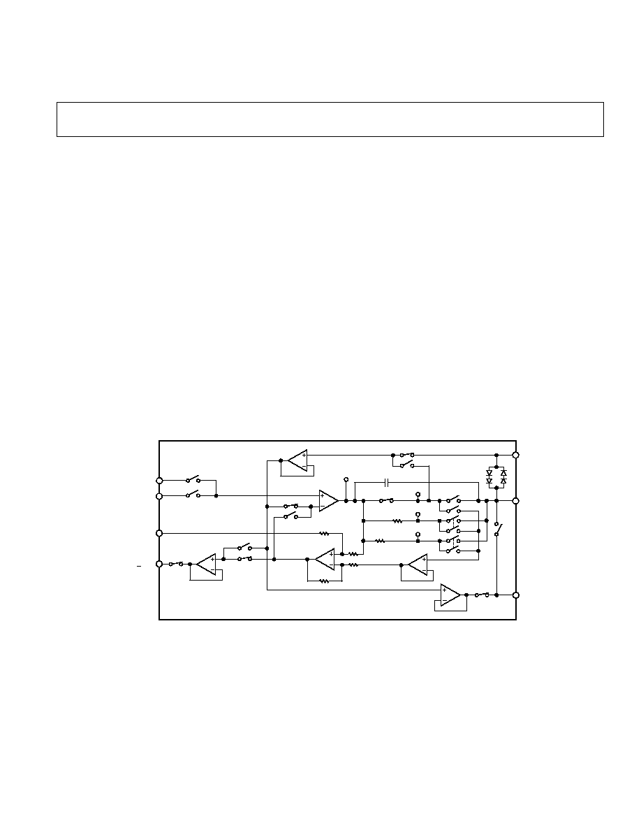
PPMU Circuit
FUNCTIONAL BLOCK DIAGRAM
S11
S12
S13
S14
S15
S16
INT/IM
R1
R2
INTEGRATE
S10
UNITY
DIFF
VF
S4
IF
S5
C1
1k
2mA
10k
200 A
EXT RC
SENSE
S8
S9
S2
S3
VM
IM
ENABLE
S1
CON
+2.5V
S6
S7
DAC1
DAC2
DSR
MEAS OUT
40pF
S17
GUARD
FORCE
SENSE
R
R
1.25R
1.25R
MAIN
GUARD
S18
AD53508
OUTPUT
FEATURES
Dual Measurement Channels
Precision Four-Quadrant-Per-Pin V/I Source
Programmable Current Force Ranges
204.8 A and 2.048 mA
Five Current Measurement Ranges
204.8 nA to 2.048 mA
Output Voltage Range: 4 V to +9 V
Power Supplies: +15 V, +5 V, and 10 V
44-Lead Plastic J-Leaded Chip Carrier Package
APPLICATIONS
Can Be Used with the AD53032 DCL to Extend Current
Force Range to 35 mA
GENERAL DESCRIPTION
The AD53508 is a custom dual-channel parametric measure-
ment circuit for use in semiconductor automatic test equipment.
It contains programmable modes to force a pin voltage and
measure its current or to integrate and hold a current value.
Alternatively, a current can be forced and the compliance volt-
age measured.
The device provides a remote force/sense capability to ensure
accuracy at the tester pin. A guard output is available to drive
the shield of a force/sense pair.
Two input references per channel permit controlled switching to
different voltage or current levels. The forced voltage or current
levels can be switched back to the measurement system to read
back the analog levels for system calibration.
The circuit is powered by +15 V, +5 V and 10 V supplies and
dissipates 230 mW nominally.
Recommended Use of the PPMU with AD53032 DCL
The PPMU can be used with the AD53032 DCL to extend the
Current Force Range beyond 2 mA VCOM can be set to the
maximum spec allowance of 8 V, which would allow the maxi-
mum Current Force of IOL of 35 mA. The combination of the
PPMU and the DCL would have a few benefits including:
1. Accurately measuring low currents.
2. Can take parallel measurements by using one PMU per pin.

2
REV. 0
AD53508SPECIFICATIONS
Parameter
Condition
Min
Typ
Max
Unit
1
VOLTAGE FORCE/MEASURE MODE
Voltage Swing,
±2 mA Range
±2 mA Drive
4
+9
V
±100 µA Drive
5
+12
V
ACCURACY
Gain (
±0.1% Tolerance)
0.999
1.001
V/V
Offset Error
±15
mV
Gain Nonlinearity (Relative to Endpoints)
±0.02
% of Span
Current Measure CMRR (at MEAS_OUT)
±0.31
mV/V
DRIFT
Gain Error Temperature Coefficient
±20
ppm (PV
or MV)/
°C
Offset Drift
±100
µV/°C
CURRENT FORCE/MEASURE MODE RANGES
0 (High)
±2.0
mA
1 (Low)
±200
µA
ACCURACY--HIGH RANGE
Transconductance (
±3% Tolerance)
Force Mode
0.776
0.8
0.824
mA/V
Transresistance (
±3% Tolerance)
Measure Mode
1.21
1.25
1.29
V/mA
Offset Error
±40
µA
Gain Nonlinearity (Relative to Endpoints)
±0.05
% of Span
Output Compliance Voltage-Induced
Transconductance/Error
Force Mode
0.2
+0.4
µA/V
DRIFT--HIGH RANGE
Gain Error Temperature Coefficient
+10/60
ppm (PV
or MV)/
°C
Offset Drift
±400
nA/
°C
ACCURACY--LOW RANGE
Transconductance (
±3% Tolerance)
Force Mode
77.6
80
82.4
µA/V
Transresistance (
±3% Tolerance)
Measure Mode
12.1
12.5
12.9
V/mA
Offset Error
±4
µA
Gain Nonlinearity (Relative to Endpoints)
±0.05
% of Span
Output Compliance Voltage-Induced
Transconductance/Error
Force Mode
0.02
+0.04
µA/V
DRIFT--LOW RANGE
Gain Error Temperature Coefficient
+10/60
ppm (PV
or MV)/
°C
Offset Drift
±40
nA/
°C
CURRENT MEASURE INTEGRATE MODE RANGES
High
±20.0
µA
Medium
±2.0
µA
Low
±200
nA
ACCURACY--HIGH RANGE
Transresistance Error (
±3% Tolerance)
0.121
0.125
0.129
V/
µA
Offset Error
±400
nA
Gain Nonlinearity (Relative to Endpoints)
±0.05
% of Span
Output Compliance Voltage-Induced Transresistance Error
±2.5
nA/V of Output
DRIFT--HIGH RANGE
Gain Error Temperature Coefficient
±20
ppm MV/
°C
Offset Drift
±2
nA/
°C
ACCURACY--MEDIUM RANGE
Transresistance Error (
±3% Tolerance)
1.21
1.25
1.29
V/
µA
Offset Error
±40
nA
Gain Nonlinearity (Relative to Endpoints)
±0.05
% of Span
Output Compliance Voltage-Induced Transresistance Error
±0.25
nA/V of Output
DRIFT-- MEDIUM RANGE
Gain Error Temperature Coefficient
±20
ppm MV/
°C
Offset Drift
±250
pA/
°C
(T
A
= 25 C, rated power supplies unless otherwise noted)

3
REV. 0
AD53508
Parameter
Condition
Min
Typ
Max
Unit
1
ACCURACY--LOW RANGE
Transresistance Error (
±3% Tolerance)
0.0121
0.0125
0.0129
V/nA
Offset Error
±4
nA
Gain Nonlinearity (Relative to Endpoints)
±0.05
% of Span
Output Compliance Voltage-Induced Transresistance Error
±0.025
nA/V of Output
DRIFT--LOW RANGE
Gain Error Temperature Coefficient
±20
ppm MV/
°C
Offset Drift
±70
pA/
°C
DISABLE MODE
2
Voltage Swing,
±2 mA Range
±2 mA Drive
4
+9
V
±100 µA Drive
5
+12
V
ACCURACY
Gain (
±0.1% Tolerance)
0.999
1.001
V/V
Offset Error
±15
mV
Gain Nonlinearity (Relative to Endpoints)
±0.02
% of Span
Current Measure CMRR (at MEAS_OUT)
±0.31
mV/V
DRIFT
Gain Error Temperature Coefficient
±20
ppm (PV or
MV)/
°C
Offset Drift
±100
µV/°C
OTHER SPECIFICATIONS
Power Supply Rejection Ratio
f < 40 Hz, V
CC
70
dB
f < 40 Hz, V
EE
60
dB
f = 40 kHz, V
CC
35
dB
f = 40 kHz, V
EE
25
dB
CURRENT MEASURE HOLD MODE LEAKAGE
T
AMB
= +70
°C
±1.2
nA
CROSSTALK
3
±0.02
% of Span
SETTLING TIMES TO 0.01%
Voltage Force and Guard Voltage
C
LOAD
= 100 pF
20
µs
C
LOAD
= 2000 pF
2
ms
Current Force (200
µA Range)
Z
LOAD
= 100 pF 50 k
50
µs
MEAS_OUT Pin
C
LOAD
= 20 pF
2
µs
SHORT CIRCUIT CURRENT LIMIT MAGNITUDE
Any Output Except Guards
8.5
20
mA
GUARD SCC LIMIT MAGNITUDE
2.5
10
mA
GUARD OFFSET (FROM SENSE INPUT PIN)
65
25
0
mV
I
B
(DAC1, DAC2) CURRENT
±1.0
µA
DIGITAL INPUTS
V
IH
2.4
V
V
IL
0.8
V
I
IN
(Input leakage current)
10
µA
POWER SUPPLIES
V
CC
(Positive Analog Supply Voltage)
14.0
15.0
15.75
V
V
EE
(Negative Analog Supply Voltage)
10.5
10.0
9.0
V
V
DD
(Logic Supply Voltage)
4.75
5.0
5.25
V
I
CC
(Positive Analog Supply Current)
5
15
mA
I
EE
(Negative Analog Supply Current)
15
5
mA
I
DD
(Logic Supply Current Is 0 with Inputs at Rails,
Worst Case @ 2.4 V
IN
)
8
mA
NOTES
1
PV = Programmed Value, MV = Measured Value, FSR = Full-Scale Range = span.
2
Output connected: DAC2 and 2 mA range selected, unconditionally.
3
f < 40 Hz, both channels in current force mode; other channel output voltage swinging rail to rail.
Specifications subject to change without notice.
AD53508
4
REV. 0
CAUTION
ESD (electrostatic discharge) sensitive device. Electrostatic charges as high as 4000 V readily
accumulate on the human body and test equipment and can discharge without detection.
Although the AD53508 features proprietary ESD protection circuitry, permanent damage may
occur on devices subjected to high energy electrostatic discharges. Therefore, proper ESD
precautions are recommended to avoid performance degradation or loss of functionality.
WARNING!
ESD SENSITIVE DEVICE
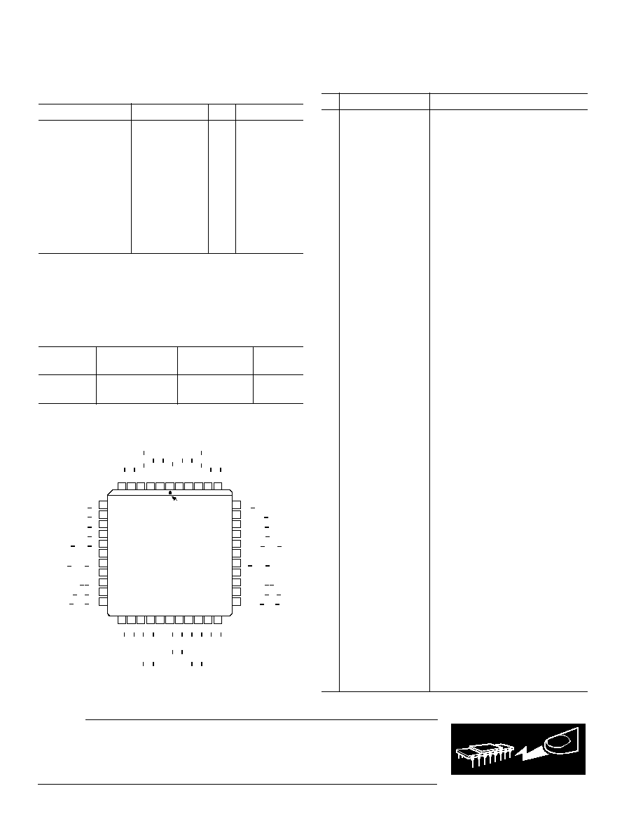
PIN FUNCTION DESCRIPTIONS
Pin Name
Description
1
DSR_2.5
2.5 V Reference Input
2
DAC2_A
First of Two Switchable Inputs
3
DAC1_A
Second of Two Switchable Inputs
4
EXT_RC_A
External R
S
and C Common
5
C1_A
External Capacitor
6
R1_A
External Resistor
7
R2_A
External Resistor
8
SENSE_A
Sense Input
9
FORCE_A
Force Output
10
GUARD_A
Guard Drive Output
11
MEAS_OUT_A
Measurement Output
12
VCC
+15 V Analog Supply
13
M_CON_A
*
Connect Measure Output to Bus
14
VEE
10 V Analog Supply
15
FORCE_I_A
*
Force V (When Hi) or I (When Lo)
16
FORCE_EN_A
*
Control Input
17
DAC1_SEL_A
*
Select DAC1 (When Lo) or DAC2
18
INTEG_A
*
Control Input
19
HOLD_A
*
Control Input
20
I_RANGE0_A
*
Select 2 mA Range (Active Lo)
21
I_RANGE1_A
*
Select 200
µA Range (Active Lo)
22
VERIFY*
Measure Forced Voltage or Current
23
OUTPUT_CON_A
*
Connect Pin Drive (Active Lo)
24
OUTPUT_CON_B
*
Connect Pin Drive (Active Lo)
25
I_RANGE1_B
*
Select 200
µA Range (Active Lo)
26
I_RANGE0_B
*
Select 2 mA Range (Active Lo)
27
HOLD_B
*
Control Input
28
INTEG_B
*
Control Input
29
DAC1_SEL_B
*
Select DAC1 (When Lo) or DAC2
30
FORCE_EN_B
*
Control Input
31
FORCE_I_B
*
Force V (When Hi) or I (When Lo)
32
DIGGND
Digital Ground
33
M_CON_B
*
Connect Measure Output to Bus
34
VDD
+5 V Digital Supply
35
MEAS_OUT_B
Measurement Output
36
GUARD_B
Guard Drive Output
37
FORCE_B
Force Output
38
SENSE_B
Sense Input
39
R2_B
External Resistor
40
R1_B
External Resistor
41
C1_B
External Capacitor
42
EXT_RC_B
External R
S
and C Common
43
DAC1_B
Second of Two Switchable Inputs
44
DAC2_B
First of Two Switchable Inputs
*
= Active Lo
ABSOLUTE MAXIMUM RATINGS
*
(T
A
= 25
°C unless otherwise noted)
Min
Max
Unit
Condition
VDD to VEE
0.3
+26.4
V
VCC to VEE
0.3
+26.4
V
VDD to DGND
0.3
+6
V
Digital Inputs to DGND 0.3
VCC+0.3 V
Power Dissipation
700
mW
T
A
+75°C
Operating Temperature
Range
25
70
°C
Storage Temperature
60
+125
°C
Lead Temperature
+300
°C
Soldering (10 sec)
Force/Sense Outputs
VEE0.8 VCC+0.8 V
Or 75 mA,
Whichever Is Less
*
Stresses above those listed under Absolute Maximum Ratings may cause perma-
nent damage to the device. These are stress ratings only; functional operation of
the device at these or any other conditions above those indicated in the operational
sections of this specification is not implied. Exposure to absolute maximum rating
conditions for extended periods may affect device reliability.
ORDERING GUIDE
Temperature
Package
Package
Model
Range
Description
Option
AD53508JP
25
°C to 70°C
Plastic Leaded
P-44A
Chip Carrier
PIN CONFIGURATION
6 5 4 3 2 1 44 43 42 41 40
PIN 1
IDENTIFIER
TOP VIEW
(Not to Scale)
39
38
37
36
35
34
33
32
31
30
29
7
8
9
10
11
12
13
14
15
16
17
18 19 20 21 22 23 24 25 26 27 28
* = ACTIVE LO
R2 B
SENSE B
FORCE B
GUARD B
MEAS OUT B
VDD
M CON B*
DIGGND
FORCE I B*
FORCE EN B*
DAC1 SEL B*
R2 A
SENSE A
FORCE A
GUARD A
MEAS OUT A
VCC
M CON A*
VEE
FORCE I A*
FORCE EN A*
DAC1 SEL A*
R1
A
C1
A
EXT
RC
A
DAC1
A
DAC2
A
DSR
2.5
DAC2
B
INTEG
A*
HOLD
A*
I
RANGE0
A*
I
RANGE1
A*
OUTPUT
CON
A*
OUTPUT
CON
B*
I
RANGE1
B*
I
RANGE0
B*
HOLD
B*
INTEG
B*
VERIFY*
DAC1
B
EXT
RC
B
C1
B
R1
B
AD53508
AD53508
5
REV. 0
Table I. Data Table
Data Latch Bits
S13,
S15,
S1
S2
S3
S4
S5
S6
S7
S9
S17
S8
S10
S14
S16
S11
S12
S18
Voltage Force/Current Measure
Irange 0
On
Off
On
On
Off
On
Off
Off
Off
On
On
On
Off
Off
Off
On
Irange 1
On
Off
On
On
Off
On
Off
Off
Off
On
On
Off
On
Off
Off
On
Integrate Range
On
Off
On
On
Off
On
Off
Off
Off
On
On
Off
Off
On
On
On
Integrate
On
Off
On
On
Off
On
Off
Off
Off
On
Off
Off
Off
On
On
On
Hold/Measure
On
Off
On
On
Off
On
Off
On
On
Off
Off
Off
Off
Off
On
On
Current Force/Voltage Measure
Irange 0
On
On
Off
Off
On
On
Off
Off
Off
On
On
On
Off
Off
Off
On
Irange 1
On
On
Off
Off
On
On
Off
Off
Off
On
On
Off
On
Off
Off
On
Disable Mode: Output Connected
X
X
X
On
Off
Off
On
Off
Off
On
X
On
Off
Off
Off
On
Verify/Voltage Force
On
On
Off
On
Off
On
Off
Off
Off
On
On
On
Off
Off
Off
On
Verify/Current Force
On
Off
On
Off
On
On
Off
Off
Off
On
On
On
Off
Off
Off
On
Disconnect
X
X
X
On
Off
X
X
On
Off
Off
On
Off
Off
Off
On
Off
DAC2 Select: Enabled
X
X
X
X
X
Off
On
X
X
X
X
X
X
X
X
X
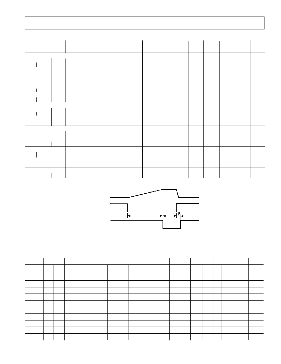
CAPACITOR
CHARGE
INTEGRATE*
HOLD*
INTEGRATE
HOLD
DISCHARGE
CAPACITOR
* = ACTIVE LO
Figure 1. Integrate/Current Measure Timing Diagram
Table II. Truth Table
* = Active LO
FV/MI 2 mA
FV/MI 200 mA
FV/MI Integrate DAC1
FV/MI Integrate DAC 2
FI/MV 2 mA
FI/MV 200
µA
FV/Verify
FI/Verify
Disconnect
Disable
Control
Voltage
Inte-
Voltage
Inte-
Output
Input
DAC1
DAC2
DAC1
DAC2
Settle
grate
Hold
Settle
grate
Hold
DAC1
DAC2
DAC1
DAC2
DAC1
DAC2
DAC1
DAC2
Connected
M_CON*
LO
LO
LO
LO
LO
LO
LO
LO
LO
LO
LO
LO
LO
LO
LO
LO
LO
LO
X
X
VERIFY*
HI
HI
HI
HI
HI
HI
HI
HI
HI
HI
HI
HI
HI
HI
LO
LO
LO
LO
X
X
FORCE_I*
HI
HI
HI
HI
HI
HI
HI
HI
HI
HI
LO
LO
LO
LO
HI
HI
LO
LO
X
X
FORCE_EN*
LO
LO
LO
LO
LO
LO
LO
LO
LO
LO
LO
LO
LO
LO
LO
LO
LO
LO
X
HI
DAC1_SEL*
LO
HI
LO
HI
LO
LO
LO
HI
HI
HI
LO
HI
LO
HI
LO
HI
LO
HI
X
X
INTEG*
HI
HI
HI
HI
HI
LO
LO
HI
LO
LO
HI
HI
HI
HI
HI
HI
HI
HI
X
X
HOLD*
HI
HI
HI
HI
HI
HI
LO
HI
HI
LO
HI
HI
HI
HI
HI
HI
HI
HI
X
X
I_RANGE0*
LO
LO
HI
HI
HI
HI
HI
HI
HI
HI
LO
LO
HI
HI
X
X
X
X
X
X
I_RANGE1*
HI
HI
LO
LO
HI
HI
HI
HI
HI
HI
HI
HI
LO
LO
X
X
X
X
X
X
OUTPUT_CON*
LO
LO
LO
LO
LO
LO
LO
LO
LO
LO
LO
LO
LO
LO
LO
LO
LO
LO
HI
LO