 | ÐлекÑÑоннÑй компоненÑ: AD53522 | СкаÑаÑÑ:  PDF PDF  ZIP ZIP |
AD53522 High Speed Dual Pin Electronic Data Sheet (REV. A)
REV. A
a
AD53522
Information furnished by Analog Devices is believed to be accurate and
reliable. However, no responsibility is assumed by Analog Devices for its
use, nor for any infringements of patents or other rights of third parties that
may result from its use. No license is granted by implication or otherwise
under any patent or patent rights of Analog Devices. Trademarks and
registered trademarks are the property of their respective owners.
One Technology Way, P.O. Box 9106, Norwood, MA 02062-9106, U.S.A.
Tel: 781/329-4700
www.analog.com
Fax: 781/326-8703
© 2003 Analog Devices, Inc. All rights reserved.
High Speed
Dual Pin Electronic
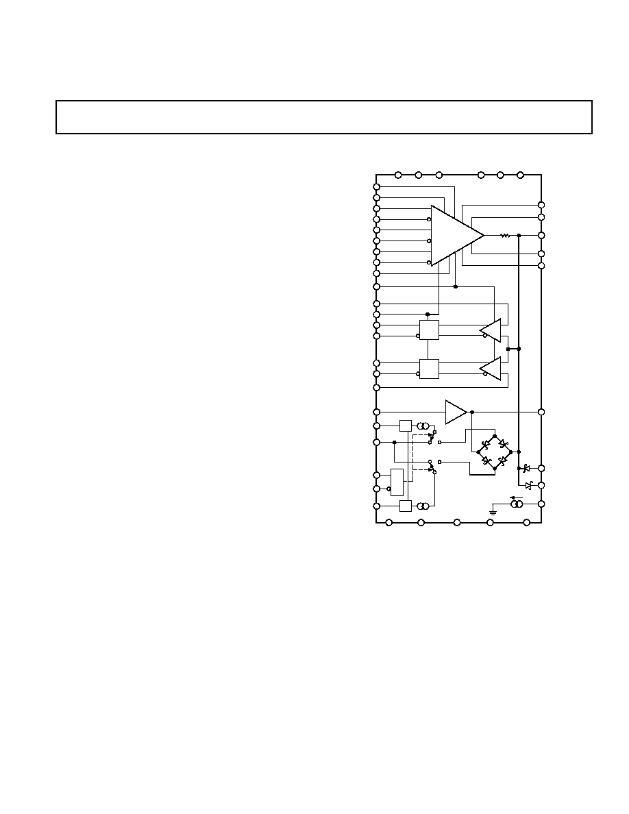
FUNCTIONAL BLOCK DIAGRAM (One-Half)
DRIVER
COMPARATOR
V/I
V/I
ACTIVE LOAD
1.0 A/ K
V
CC
V
CC
V
CC
V
EE
V
EE
V
EE
AD53522
VHDCPL
OUT
VLDCPL
PWRGND
9
HQGND
VCOM_S
THERM*
+1
VH
VTERM
DATA
IOD
RLD
VL
HCOMP
VCCO
QH
QL
LCOMP
VCOM
IOLC
IOXRTN
INHL
IOHC
VCL
VCH
PROT_HI
PROT_LO
PWRD
GND_ROT
DR_GND
THERMSTART
*ONLY 1 (ONE) THERM PER DEVICE
INHLB
QLB
QHB
RLDB
IODB
DATAB
FEATURES
1000 MHz Toggle Rate
Driver/Comparator/Active Load and Dynamic Clamp
Included
Inhibit Mode Function
100-Lead LQFP Package with Built-In Heat Sink
Driver
48 Output Resistance
800 ps Tr/Tf for a 3 V Step
Comparator
1.1 ns Propagation Delay at 3 V
Load
40 mA Voltage Programmable Current Range
50 ns Settling Time to 15 mV
APPLICATIONS
Automatic Test Equipment
Semiconductor Test Systems
Board Test Systems
Instrumentation and Characterization Equipment
PRODUCT DESCRIPTION
The AD53522 is a complete, high speed, single-chip solution
that performs the pin electronics functions of driver, comparator,
and active load (DCL) for ATE applications. In addition, the
driver contains a dynamic clamp function and the active load
contains an integrated Schottky diode bridge.
The driver is a proprietary design that features three active states:
Data High mode, Data Low mode, and Term mode, as well as
an Inhibit State. In conjunction with the integrated dynamic
clamp, this facilitates the implementation of a high speed active
termination. The output voltage range is 0.5 V to +6.5 V to
accommodate a wide variety of test devices.
The dual comparator, with an input range equal to the driver
output range, features PECL compatible outputs. Signal tracking
capability is in the range of 3 V/ns.
The active load can be set for up to 40 mA load current. I
OH
, I
OL
,
and the buffered VCOM are independently adjustable. On-board
Schottky diodes provide high speed switching and low capacitance.
Also included is an on-board temperature sensor that gives an
indication of the silicon surface temperature of the DCL. This
information can be used to measure
JC
and
JA
or flag an alarm
if proper cooling is lost. Output from the sensor is a current sink
that is proportional to absolute temperature. The gain is trimmed
to a nominal value of 1.0
µA/K. As an example, the output current
can be sensed by using a 10 k
resistor connected from 10 V to
the THERM (I
OUT
) pin. A voltage drop across the resistor will
be developed that equals 10 k
1 µA/°K = 10 mV/°K = 2.98 V
at room temperature.

REV. A
2
AD53522SPECIFICATIONS
DRIVER
1
(T
J
= 85 C
5 C, +V
S
= +10.5 V
1%, V
S
= 4.5 V
1%, VCCO = 3.3 V, unless otherwise noted.)
Spec
Spec
3
No.
Parameter
Conditions
Min
Typ
2
Max
Unit
Perf
DIFFERENTIAL INPUT CHARACTERISTICS
(DATA to DATAB, IOD to IODB, RLD to RLDB)
1
Voltage Range
Note: Inputs are from Same Logic
0
+3.3
V
N
Type Family
2
Differential Voltage with
Note: AC Tests Performed
±400
±600
±1000
mV
P
LVPECL Levels
3
Bias Current
V
IN
= 1.5 V, 2.5 V
250
+250
µA
P
REFERENCE INPUTS
4
Bias Currents
Max Value Measured during
50
+50
µA
P
Linearity Tests
OUTPUT CHARACTERISTICS
10
Logic High Range
Data = H, VH = 0.4 V to +6.5 V,
0.4
+6.5
V
P
Vl = 0.5 V (VT = 0 V, VH Meets
Test 20, 21, and 22 Specs)
11
Logic Low Range
Data = L, VL = 0.5 V to +6.4 V,
0.5
+6.4
V
P
VH = 6.5 V (VT = 0 V, VL Meets
Test 30, 31, and 32 Specs)
12
Amplitude [VHVL]
VL = 0.05 V, VH = +0.05 V,
+0.1
+7.0
V
P
VT = 0 V and VL = 0.5 V,
VH = +6.5 V, VT = 0 V
ABSOLUTE ACCURACY
20
VH Offset
Data = H, VH = 0 V, VL = 0.5 V,
50
+50
mV
P
VT = +3 V
21
VH Gain Error
Data = H, VH = 0.4 V to +6.5 V,
0.3
+0.3
% of VH
P
VL = 0.5 V, VT = +3 V
22
Linearity Error
Data = H, VH = 0.4 V to +6.5 V,
5
+5
mV
P
VL = 0.5 V, VT = +3 V
30
VL Offset
Data = L, VL = 0 V, VH = +6.5 V,
50
+50
mV
P
VT = +3 V
31
VL Gain Error
Data = L, VL = 0.5 V to +6.4 V,
0.3
+0.3
% of VL
P
VH = +6.5 V, VT = +3 V
32
Linearity Error
Data = L, VL = 0.5 V to +6.4 V,
5
+5
mV
P
VH = +6.5 V, VT = +3 V
33
Offset Temperature Coefficient
VL = 0 V, VH = +5 V, VT = 0 V
+0.5
mV/
°C
N
OUTPUT RESISTANCE
40
VH = 0.3 V
VL = 0.5 V, VT = 0 V, I
OUT
= +1,
+46
+50
N
+30 mA
41
VH = +6.5 V
VL = 0.5 V, VT = 0 V, I
OUT
= 1,
+46
+50
P
30 mA
42
VL = 0.5 V
VH = +6.5 V, VT = 0 V, I
OUT
= +1,
+46
+50
P
+30 mA
43
VL = +6.4 V
VH = +6.5 V, VT = 0 V, I
OUT
= 1,
+46
+50
N
30 mA
44
VH = +2.5 V
VL = 0 V, VT = 0 V, I
OUT
= 30 mA
+47.5
P
(Trim Point)
50
Dynamic Current Limit
Cbyp = 39 nF, VH = +6.5 V,
+100
mA
N
VL = 0.5 V, VT = 0 V
51
Static Current Limit
Output to 0.5 V, VH = +6.5 V,
120
60
mA
P
VL = 0.5 V, VT = 0 V, DATA = H
52
Static Current Limit
Output to +6.5 V, VH = +6.5 V,
+60
+120
mA
P
VL = 0.5 V, VT = 0 V, DATA = L

REV. A
3
AD53522
DRIVER
1
(continued)
Spec
Spec
3
No.
Parameter
Conditions
Min
Typ
2
Max
Unit
Perf
VTERM
60
Voltage Range
Term Mode, VTERM = 0.3 V
0.3
+6.3
V
P
to +6.3 V, VL = 0 V, VH = +3 V
(VTERM Meets Test 61, 62, and 63 specs)
61
VTERM Offset
Term Mode, VTERM = 0 V,
50
+50
mV
P
VL = 0 V, VH = +3 V
62
VTERM Gain Error
Term Mode, VTERM = 0.3 V
0.3
+0.3
% of V
SET
P
to +6.3 V, VL = 0 V, VH = +3 V
63
VTERM Linearity Error
4
Term Mode, VTERM = 0.3 V
5
+5
mV
P
to +6.3 V, VL = 0 V, VH = +3 V
64
Offset Temperature Coefficient
VTERM = 0 V, VL = 0 V, VH = +3 V
+0.5
mV/
°C
N
70
Output Resistance DC
I
OUT
= +30 mA, 1 mA,
+46
+50
VTERM = 0.3 V, VH = +3 V, VL = 0 V
N
I
OUT
= 30 mA, +1 mA,
VTERM =+6.3 V, VH = +3 V, VL = 0 V
N
I
OUT
=
±30 mA, ±1 mA,
VTERM = +2.5 V, VH = +3 V, VL = 0 V
P
72
PSRR, Drive, or Term Mode
+V
S
, V
S
± 1%
+17.8
mV/V
N
73
Static Current Limit
Output to 0.3 V, VTERM = +6.3 V
120
60
mA
P
74
Static Current Limit
Output to +6.3 V, VTERM = 0.3 V
+60
+120
mA
P
DYNAMIC PERFORMANCE, DRIVE (VH and VL)
80
Propagation Delay Time
Measured at 50%, VL = 0 V,
1.25
1.4
1.55
ns
P
VH = 3 V, into 500
81
Propagation Delay T.C.
Measured at 50%, VL = 0 V,
2
ps/
°C
N
VH = 3 V, into 500
82
Delay Matching, Edge-to-Edge
Measured at 50%, VL = 0 V,
200
ps
P
VH = 3 V, into 500
RISE AND FALL TIMES
90
200 mV Swing
Measured 20%80%, VL = 0.1 V,
0.25
ns
N
VH = +0.1 V, into 50
91
1 V Swing
Measured 20%80%, VL = 0 V,
0.3
ns
N
VH = 1 V, into 50
92
3 V Swing
Measured 10%90%, VL = 0 V,
0.8
ns
N
VH = 3 V, into 50
93
3 V Swing
Measured 10%90%, VL = 0 V,
0.8
ns
N
VH = 3 V, into 500
93A
3 V Swing
Measured 20%80%, VL = 0 V,
0.450
0.560
0.670
ns
P
VH = 3 V, into 500
94
5 V Swing
Measured 10%90%, VL = 0 V,
1.2
1.5
ns
N
VH = 5 V, into 500
RISE AND FALL TIME TEMPERATURE COEFFICIENT
100
1 V Swing
(Per Test 91)
±2
ps/
°C
N
101
3 V Swing
(Per Test 92)
±2
ps/
°C
N
102
5 V Swing
(Per Test 94)
±4
ps/
°C
N
110
Overshoot and Preshoot
VL, VH = 0.1 V, +0.1 V,
0 50
0 + 50
% of Step N
Driver Terminated into 50
+ mV
VL, VH = 0.0 V, 3 V,
6.0 50
+6.0 + 50 % of Step N
Driver Terminated into 50
+ mV
SETTLING TIME
120
to 15 mV
VL = 0 V, VH = 0.5 V,
50
ns
N
Driver Terminated into 50
121
to 4 mV
VL = 0 V, VH = 0.5 V
10
µs
N
130
Delay Change vs. Pulse Width
VL/VH = 0/3, PW = 2.5 ns/7.5 ns,
25
75
ps
N
30 ns/90 ns, DC = 25%
131
Delay Change vs. Duty Cycle
VL = 0 V, VH = 3 V, Duty Cycle
25
ps
N
(DC) 5% to 95%, T = 40 ns

REV. A
4
AD53522
SPECIFICATIONS
(continued)
DRIVER
1
(continued)
Spec
Spec
3
No.
Parameter
Conditions
Min
Typ
2
Max
Unit
Perf
MINIMUM WIDTH PULSE
140
1 V Swing
Measured at 50% point width
0.6
ns
N
V
OUT
AC Swing = 0.9
V
OUT
DC
141
3 V Swing
Swing Terminated, 50
Load on
1.5
ns
N
Transmission Line
142
Toggle Rate
VH = 1 V, VL = 0 V, Terminated
1000
MHz
N
to 50
,V
OUT
> 300 mV p-p
DYNAMIC PERFORMANCE, INHIBIT
150
Delay Time, Active to Inhibit
Measured at 50%, VH = 4 V,
1.7
2.0
ns
P
VL = 0 V, VTT = 2
151
Delay Time, Inhibit to Active
Measured at 50%, VH = 4 V,
1.7
2.2
ns
P
VL = 0 V, VTT = 2
152
Delay Time Matching,
Measured at 50%, VH = 4 V,
150
250
ps
P
Inhibit to Active
VL = 0 V, VTT = 2
153
Delay Time Matching,
Measured at 50%, VH = 4 V,
150
250
ps
P
Active to Inhibit
VL = 0 V, VTT = 2
160
I/O Spike
VH = 0 V, VL = 0 V
200
mV p-p
N
170
Rise, Fall Time, Active to Inhibit
VL = 0 V, VTT = 2
1.2
ns
N
(20%80% of 1 V Output)
171
Rise, Fall Time, Inhibit to Active
VH = 4 V, VL = 0 V, VTT = 2
0.6
ns
N
(20%80% of 1 V Output)
DYNAMIC PERFORMANCE, VTERM
180
Delay Time, VH to VTERM
Measured at 50%, VL = VH = 2 V,
1.5
1.9
ns
P
VTERM = 0 V, VTT = 0 V
181
Delay Time, VL to VTERM
Measured at 50%, VL = VH = 0 V,
1.6
1.9
ns
P
VTERM = 2 V, VTT = 0 V
182
Delay Time, VTERM to VH
Measured at 50%, VL = VH = 2 V,
1.6
2.0
ns
P
VTERM = 0 V, VTT = 0 V
183
Delay Time, VTERM to VL
Measured at 50%, VL = VH = 0 V,
1.6
2.0
ns
P
VTERM = 2 V, VTT = 0 V
190
Overshoot and Preshoot
VH/VL, VTERM = (0 V, 2 V),
6.0 + 50
+6.0 + 50 % of Step N
(0 V, 6 V)
+ mV
191A
VTERM Rise Time, VL to VT,
VL, VH = 0 V, VTERM = 2 V,
1.0
ns
N
Normal Mode
20%80%
191B
VTERM Rise Time, VT to VH,
VL, VH = 2 V, VTERM = 0 V,
0.6
ns
N
Normal Mode
20%80%
192A
VTERM Fall Time, VT to VL,
VL, VH = 0 V, VTERM = 2 V,
0.6
ns
N
Normal Mode
20%80%
192B
VTERM Fall Time, VH to VT,
VL, VH = 2V, VTERM = 0 V,
1.0
ns
N
Normal Mode
20%80%

REV. A
5
AD53522
COMPARATOR
1
Spec
Spec
3
No.
Parameter
Conditions
Min
Typ
2
Max
Unit
Perf
DC INPUT CHARACTERISTICS
200
VCCO Range
+2.0
+4.5
V
N
201
Offset Voltage (V
OS
)
Common-Mode Voltage = 0 V
25
+25
mV
P
202
Offset Voltage Drift
Common-Mode Voltage = 0 V
+50
µV/°C N
203
HCOMP, LCOMP
Over Linearity Range
50
+50
µA
P
BIAS CURRENTS
206
Voltage Range (V
CM
)
0.5
+6.5
V
P
207
Differential Voltage (V
DIFF
)
+7
V
P
208
Gain Error
V
IN
= 0.5 V to +6.5 V
0.25
0.0
%FSR
N
209
Linearity Error
V
IN
= 0.5 V to +6.5 V
2
+2
mV
N
210
Extended Range Operation
HCOMP, LCOMP = 1, Output
1.0
V
P
Toggle V
OUT
from 0.9 V to 1.1 V
DIGITAL OUTPUTS
220
Logic 1 Voltage Q
Q or QB, 150
to GND,
VCCO 1.05
VCCO 0.85
V
P
150
from Q to QB
221
Logic 0 Voltage QB
Q or QB, 150
to GND,
VCCO 2.2
VCCO 1.5
V
P
150
from Q to QB
222
Logic Differential, QQB
Q or Qb, 150
to GND,
0.65
0.9
1.15
V
P
150
from Q to QB
225
Slew Rate
Q or QB (20% 80% of output,
380
ps
N
150
from Q to QB)
CHANNEL COMPARATOR SWITCHING PERFORMANCE
PROPAGATION DELAY
5, 6, 7
240
Input to Output
V
IN
= 3 V p-p, 2 V/ns
0.7
1.1
ns
P
241
Propagation Delay Tempco
V
IN
= 3 V p-p, 2 V/ns
1.0
ps/
°C
N
Prop Delay Change with respect to:
250
Slew Rate: 1, 2, 3 V/ns
V
IN
= 0 V to 3 V
120
ps
N
260
Amplitude: 500 mV, 1.0 V, 3.0 V
V
IN
= 1.0 V/ns
100
ps
N
270
Equivalent Input Rise Time
V
IN
= 0 V to 2 V, < 80 ps,
275
ps
N
20%80% Rise Time
Driver in VTERM = 0 V
280
Pulse Width Linearity
V
IN
= 0 V to 3 V, 2 V/ns, PW =
50
ps
N
3, 4, 5, 10 ns, Driver Hi-Z mode
281
Settling Time
Settling to
±8 mV, V
IN
= 0 V to
25
ns
N
3 V, Driver Hi-Z mode
282
Hysteresis
6
mV
N
290
Comparator Propagation Delay
V
IN
= 0 V to 3 V, 2 V/ns
125
ps
P
Matching, HCOMP to LCOMP
INPUT CHARACTERISTICS (INHL, INHLB)
See Driver Spec No. 1
300
Input Voltage
VIOH = 1 V, VIOL = 1 V,
0
+3.3
V
P
VCOM = 2 V, VDUT = 0 V
301
INHL, INHLB Bias Current
INHL, INHLB = 0 V, 3.3 V,
250
+250
µA
P
AC Tests 0.2 V and 0.8 V
302
VIOH Current Program Range,
VDUT = 0.8 V, 6.5 V
0
+4.0
V
P
IOH = 0 mA to 40 mA

REV. A
6
AD53522
SPECIFICATIONS
(continued)
ACTIVE LOAD
1
Spec
Spec
3
No.
Parameter
Conditions
Min
Typ
2
Max
Unit
Perf
303
VIOL Current Program Range,
IOL = 0 mA to 40 mA
VDUT = 0.5 V, +5.2 V
0
4.0
V
P
304
VIOH, VIOL Input Bias Current
VIOL = 0 V, 4 V and
300
+300
µA
P
VIOH = 0 V, 4 V
305
IOXRTN Range
IOL = +40 mA, IOH = 40 mA,
0.5, +6.5
V
N
VDUT = 0.5 V, +6.5 V
310
VDUT Range
IOL = +40 mA, IOH = 40 mA,
0.5
+6.5
V
P
|VDUT VCOM|> 1.3 V
311
VDUT Range,
VDUT VCOM > 1.3 V
+0.8
+6.5
V
P
IOH = 0 mA to 40 mA
312
VDUT Range,
VCOM VDUT > 1.3 V
0.5
+5.2
V
P
IOL = 0 mA to +40 mA
OUTPUT CHARACTERISTICS
Accuracy
320
Gain Error, Load Current,
IOL, IOH = 25
µA 40 mA,
0.35
+0.35
%I
SET
P
Normal Range Calculated at
VCOM = 0 V, VDUT =
±2 V, and
1 mA and 40 mA points
2
IOL = 25
µA to 40 mA, VCOM = +6.5 V,
VDUT = +5.2 V and IOH = 25
µA to
40 mA, VCOM = 0.5 V, VDUT = +0.8 V
321
Load Offset
Calculated from Intercept of 1 mA
300
+300
µA
P
and 40 mA Points
322
Load Nonlinearity
IOL, IOH from 25
µA to 40 mA
80
+80
µA
P
323
Output Current Tempco
Measured at IOH, IOL = 200
µA
<
±3
µA/°C
N
324
IOH Extended Range
Driver Inhibited, IOH = 1 mA,
2
%
P
Change in IOH from VTT = 0 V to
VTT = 1.0 V
VCOM BUFFER
330
VCOM Buffer Offset Error
IOL, IOH = 40 mA, VCOM = 0 V
50
+50
mV
P
331
VCOM Buffer Bias Current
VCOM = 0 V
20
+20
µA
P
332
VCOM Buffer Gain Error
IOL, IOH = 40 mA,
4
+4
%
P
VCOM = 0.5 V to +6.5 V
333
VCOM Buffer Linearity Error
IOL, IOH = 40 mA,
10
+10
mV
P
VCOMI = 0.5 V to +6.5 V
DYNAMIC PERFORMANCE
Propagation Delay
340
±I
MAX
to INHIBIT
VTT = +2 V, VCOM = +4 V/0 V,
1.0
1.3
2.0
ns
P
IOL = +20 mA, IOH = 20 mA
341
INHIBIT to
±I
MAX
VTT= +2 V, VCOM = +4 V/0 V,
1.2
1.8
2.4
ns
P
IOL = +20 mA, IOH = 20 mA
342
Propagation Delay Matching
Matching = (Test 340 Value)
1.0
+1.0
ns
P
(Test 341 Value)
350
I/O Spike
VCOM = 0 V, IOL = +20 mA,
250
mV
N
IOH = 20 mA
360
Settling Time to 15 mV
IOL = +20 mA, IOH = 20 mA,
50
ns
N
50
Load, to ±15 mV
361
Settling Time to 4 mV
IOL = +20 mA, IOH = 20 mA,
10
µs
N
50
Load, to ±4 mV

REV. A
7
AD53522
DYNAMIC CLAMP
1
Spec
Spec
3
No.
Parameter
Conditions
Min
Typ
2
Max
Unit
Perf
400
Input Voltage VCH
2
7.5
V
P
401
Input Voltage VCL
1.5
+4
V
P
402
Input Bias Current VCH/VCL
Overrange Spec 401, 402
250
+250
µA
P
410
VCH, VCL Offset Error
I
TEST
= 1 mA
250
+250
mV
P
411
VCH, VCL Gain Error
I
TEST
= 1 mA
0.96
1.01
V/V
P
420
Static Current Capability
50
75
mA
N
430
Incremental Resistance
11 mA to 21 mA
45
48
52
P
440
VCHP, VCLP Protection
0.52
0.64
V
P
Diodes Vf @ 500
µA
441
Protection Diodes Max Current
For Information Only
2
mA
N
TOTAL FUNCTION
Spec
Spec
3
No.
Parameter
Conditions
Min
Typ
2
Max
Unit
Perf
500
PWRD Input Voltage
0
5
V
P
501
PWRD Bias Current
PWRD Trip Point 1.4 V
± 0.15 V
250
+250
µA
P
503
Power-Down Supply Reduction
VIOH = 0 V, VIOL = 0 V
35
60
%
P
504
Power-Down Output
VIOH = 0 V, VIOL = 0 V,
20
+20
nA
P
Leakage Current
V
OUT
= 0.5 V to +5.5 V
505
Power-Down Output
VIOH = 0 V, VIOL = 0 V,
500
+500
nA
P
Leakage Current
V
OUT
= 5.5 V to 6.5 V
600
Output Leakage Current
V
OUT
= 0.5 V to +6.5 V
1
+1
µA
P
601
Output Leakage Current
V
OUT
= 0 V to 5 V
500
+500
nA
P
602
Output Leakage Current
V
OUT
= 1 V
5
+5
µA
P
605
Output Capacitance
Driver and Load Inhibited
9.2
pF
N
606
Output Capacitance Term
Driver VTERM = 0 V, Load Inhibited
2.5
pF
N
POWER SUPPLIES
Spec
Spec
3
No.
Parameter
Conditions
Min
Typ
2
Max
Unit
Perf
610
Total Supply Range
15
V
N
620
Positive Supply, VCC
+10.5
V
N
630
Negative Supply, VEE
4.5
V
N
640
Positive Supply Current, VCC
Driver = Inhibit, I
LOAD
Program = 40 mA,
465
570
mA
P
Load = Active
650
Negative Supply Current, VEE
Driver = Inhibit, I
LOAD
Program = 40 mA,
475
600
mA
P
Load = Active
651
Comparator Supply Current
Driver = Inhibit, I
LOAD
Program = 40 mA,
45
mA
P
Overhead, VCCO
Load = Active (I
VCCO
(comparator
logic output currents))
660
Total Power Dissipation
Driver = Inhibit, I
LOAD
Program = 40 mA,
7.2
7.9
W
P
Load = Active
661
Total Power Dissipation
Driver = Inhibit, I
LOAD
Program = 40 mA, 0 mA
5.2
5.9
W
P
700
Temperature Sensor Gain Factor
R
LOAD
= 10 k
, V
SOURCE
= 10.5 V
1
µA/°K
N
NOTES
1
All temperature coefficients are measured at T
J
= 75
°C to 95°C. In test figures, voltmeter loading is 1 M or greater, scope probe loading is 100 k in parallel with 0.6 pF.
2
Typical values are not tested or guaranteed. Nominal values are generated from design or simulation analyses and/or limited bench evaluations and are not tested or guaranteed.
3
Spec Perf: N = Nominal, O = Operating Condition, T = Typical, P = Production, Max/Min.
4
VTERM linearity over the following condition: VL 6 V < VTERM < VH + 6 V.
5
All ac input values are referred to the source end of transmission line input.
6
All ac tests are performed with driver in VTERM mode except where noted.
7
Rise time is calculated SQRT((comp out Tr)
2
(comp in Tr)
2
).
Specifications are subject to change without notice.
REV. A
8
AD53522
Table II. Comparator Truth Table
Output States
V
OUT
QH
QHB
QL
QLB
> HCOMP
> LCOMP
1
0
1
0
> HCOMP
< LCOMP
1
0
0
1
< HCOMP
> LCOMP
0
1
1
0
< HCOMP
< LCOMP
0
1
0
1
ABSOLUTE MAXIMUM RATINGS
1
POWER SUPPLY VOLTAGE
V
CC
to GND . . . . . . . . . . . . . . . . . . . . . . . . . . . . . . . 11.3 V
V
EE
to GND . . . . . . . . . . . . . . . . . . . . . . . . . . . . . . . . . . 7 V
V
CC
to V
EE
. . . . . . . . . . . . . . . . . . . . . . . . . . . . . . . . . . . 18 V
VCCO to GND . . . . . . . . . . . . . . . . . . . . . . . . . . . . . . 5.5 V
PWRGND, DRGND, GND_ROT, or HQGND . . . .
±0.4 V
OUTPUTS
V
OUT
Short Circuit Duration . . . . . . . . . . . . . . . . Indefinite
2
V
OUT
, Inhibit Mode . . . . . . . . . . . . . . . . . . . . . +8.5 V, 2 V
V
OUT
, Inhibit Mode . . . . . VL 5.5 V < V
OUT
< VH + 5.5 V
VHDCPL . . . . . . . . Do Not Connect Except for Cap to V
CC
VLDCPL . . . . . . . . Do Not Connect Except for Cap to V
EE
QH, QHB, QL, QLB Maximum I
OUT
:
Continuous . . . . . . . . . . . . . . . . . . . . . . . . . . . . . . . 50 mA
Surge . . . . . . . . . . . . . . . . . . . . . . . . . . . . . . . . . . . 100 mA
THERM . . . . . . . . . . . . . . . . . . . . . . . . . . . . . . . . 11 V, 0 V
Driver Output Capacitance, Maximum . . . . . . . . . . . . 10 pF
INPUTS
DATA, DATAB, IOD, IODB, RLD, RLDB
. . . . . . . . . . . . . . . . . . . . . . . . (V
CCO
+ 1.5 V, V
CCO
4.5 V)
INHL, INHLB, CMPD . . . . . . . . . . . . . . . 0.4 V to +5.5 V
PWRD . . . . . . . . . . . . . . . . . . . . . . . . . . . . 0.4 V to +4.5 V
DATA to DATAB, IOD to IODB, RLD to RLDB . . .
±3 V
INHL to INHLB . . . . . . . . . . . . . . . . . . . . . . . . . . . . .
±6 V
VH, VL, VTERM to GND (R
SERIES
< 500
) . +7.5 V, 1.1 V
VH to VL . . . . . . . . . . . . . . . . . . . . . . . . . . . . . +8 V, 3.5 V
(VH VTERM) and (VTERM VL) . . . . . . . . . . . . .
±8 V
Reflection Clamp High/Low . . . . . . . . . . . . . . . +8.5 V, 2 V
Protection Clamp Breakdown Voltage . . . . . . . . . . . . . . 12 V
Protection Clamp Current . . . . . . . . . . . . . . . . . . . . .
±5 mA
V
OUT
to HCOMP or LCOMP . . . . . . . . . . . . . . . . . .
±7.8 V
ENVIRONMENTAL
Operating Temperature (Junction) . . . . . . . . . . . . . . . 175
°C
Storage Temperature . . . . . . . . . . . . . . . . 65
°C to +150°C
Lead Temperature (Soldering, 10 sec)
3
. . . . . . . . . . . 260
°C
NOTES
1
Stresses above those listed under Absolute Maximum Ratings may cause perma-
nent damage to the device. This is a stress rating only; functional operation of the
device at these or any other conditions above those indicated in the operational
sections of this specification is not implied. Absolute maximum limits apply
individually, not in combination. Exposure to absolute maximum rating conditions
for extended periods may affect device reliability.
2
Output short circuit protection is guaranteed as long as proper heat sinking is
employed to ensure compliance with the operating temperature limits.
3
To ensure lead coplanarity (
±0.002 inches) and solderability, handling with bare
hands should be avoided and the device should be stored in environments at 24
°C
± 5°C (75°F ±10°F) with relative humidity not to exceed 65%.
Table I. Driver Truth Table
Output
DATA DATAB
IOD
IODB
RLD
RLDB
State
0
1
1
0
X
X
VL
1
0
1
0
X
X
VH
X
X
0
1
0
1
INH and
CLAMP
X
X
0
1
1
0
VTERM
ORDERING GUIDE
Model
Temperature Range
Package Description
Package Option
AD53522JSQ
0
°C to 70°C
100-Lead LQFP-EDQUAD
SQ-100
with Integral Heat Slug
Table III. Active Load Truth Table
Output States (Including Diode Bridge)
VDUT
INHL INHLB IOH
IOL
I(V
OUT
)
<VCOM 0
1
V(IOHC) +10 mA
V(IOLC) 10 mA
IOL
>VCOM 0
1
V(IOHC) +10 mA
V(IOLC) 10 mA
IOH
X
1
0
0
0
0
CAUTION
ESD (electrostatic discharge) sensitive device. Electrostatic charges as high as 4000 V readily
accumulate on the human body and test equipment and can discharge without detection. Although
the AD53522 features proprietary ESD protection circuitry, permanent damage may occur on
devices subjected to high energy electrostatic discharges. Therefore, proper ESD precautions are
recommended to avoid performance degradation or loss of functionality.
REV. A
9
AD53522
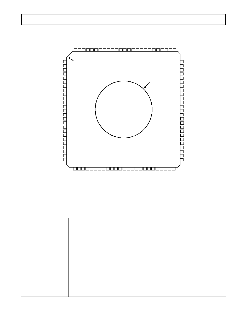
PIN CONFIGURATION
1
2
3
4
5
6
7
8
9
10
11
12
13
14
15
16
17
18
19
20
21
22
23
24
25
PROT_HI1
IOXRTN1
VCH1
VCL1
VHDCPL1
OUT1
VLDCPL1
PROT_LO1
PWRGND
PWRGND
VCOM_S1
THERM
IOLC1
IOHC1
100 99
92 91
98 97 96 95 94 93
90 89 88 87 86 85 84 83 82 81 80 79 78 77 76
HQGND
INHL1
INHLB1
V
EE
V
CC
PWRGND
RLD1
IOD1
IODB1
DATA1
DATAB1
PWRGND
PWRGND
VCOM1
VH1
VTERM1
VL1
HCOMP1
34 35
28 29 30 31 32 33
36 37 38 39 40 41 42 43 44 45 46 47 48 49 50
26 27
PROT_LO2
PWRGND
PWRGND
VCOM_S2
THERMSTART
IOLC2
IOHC2
HQGND
INHL2
INHLB2
V
EE
V
CC
PWRGND
RLD2
IOD2
IODB2
DATA2
DATAB2
PWRGND
PWRGND
V
COM2
VH2
VTERM2
VL2
HCOMP2
PWRGND
PWRGND
PWRGND
PWRGND
GND_ROT
PWRGND
PWRGND
DR_GND2
PWRGND
PWRGND
VLDCPL2
OUT2
VHDCPL2
VCL2
VCH2
IOXRTN2
PROT_HI2
LCOMP1
V
CC
V
CC
V
EE
QHB1
75
74
73
72
71
70
69
68
67
66
65
64
63
62
61
60
59
58
57
56
55
54
53
52
51
QLB1
QL1
RLDB1
PWRD1
GND_ROT
PWRD2
RLDB2
QL2
QLB2
VCCO2
QHB2
QH2
V
EE
V
EE
V
CC
V
CC
AD53522
TOP VIEW
(Not to Scale)
NOTE
DIE IS MOUNTED TO THE BACK OF THE HEAT SLUG.
THE PACKAGE IS MOUNTED TO THE BOARD, HEAT SLUG UP.
V
EE
QH1
VCCO1
LCOMP2
DR_GND
HEAT SLUG
PIN 1
IDENTIFIER
PIN FUNCTION DESCRIPTIONS
Pin Number
Mnemonic
Description
1
PROT_HI1
Channel 1, Output Voltage Sensing Diode.
2
IOXRTN1
Current Return Path for the Active Load for Channel 1. Typically connected to a power ground.
3
VCH1
Analog Input Voltage that Sets the Reflection Clamp High Level of Channel 1.
4
VCL1
Analog Input Voltage that Sets the Reflection Clamp Low Level of Channel 1.
5
VHDCPL1
Internal Supply Decoupling for the Driver Output Stage of Channel 1. This pin needs to be connected to
V
CC
through a 39 nF (minimum) capacitor.
6
OUT1
Input/Output For The Driver, Window Comparator, Reflection Clamp, and Active Load of Channel 1.
7
VLDCPL1
Internal Supply Decoupling for the Driver Output Stage of Channel 1. This pin needs to be connected to
V
EE
through a 39 nF (minimum) capacitor.
8, 9, 11, 12, 14, PWRGND
Power Ground.
15, 17, 18, 27,
28, 38, 44, 45,
81, 82, 88, 98, 99
10
DR_GND
Analog Ground.

REV. A
10
AD53522
Pin Number
Mnemonic
Description
13
GND_ROT
Analog Ground.
16
DR_GND2
Analog Ground.
19
VLDCPL2
Internal Supply Decoupling for the Driver Output Stage of Channel 2. This pin needs to be connected to
V
EE
through a 39 nF (minimum) capacitor.
20
OUT2
Input/Output for the Driver, Window Comparator, Reflection Clamp, and Active Load of Channel 2
21
VHDCPL2
Internal Supply Decoupling for the Driver Output Stage of Channel 2. This pin needs to be connected to
V
CC
through a 39 nF (minimum) capacitor.
22
VCL2
Analog Input Voltage that Sets the Reflection Clamp Low Level of Channel 2
23
VCH2
Analog Input Voltage that Sets the Reflection Clamp High Level of Channel 2
24
IOXRTN2
Current Return Path for the Active Load for Channel 2. Typically connected to a power ground.
25
PROT_HI2
Channel 2, Output Voltage Sensing Diode.
26
PROT_LO2
Channel 2, Output Voltage Sensing Diode.
29
VCOM_S2
Analog Output Voltage that Represents a Buffered VCOM1 Input
30
THERMSTART Temperature Sensor Startup Pin. Normally not connected.
31
IOLC2
Analog Input Voltage that Programs the Channel 2 Active Load Source Current.
32
IOHC2
Analog Input Voltage that Programs the Channel 2 Active Load Sink Current.
33
HQGND
Clean Analog Ground for the Active Load for Channel 2.
34
INHL2
One of Two Complementary Inputs that Control the Inhibit Mode for the Active Load Bridge of Channel 2.
35
INHLB2
One of Two Complementary Inputs that Control the Inhibit Mode for the Active Load Bridge of Channel 2.
36, 54, 55,
V
EE
Negative Supply Terminal.
71, 72, 90
37, 52, 53,
V
CC
Positive Supply Terminal.
73, 74, 89
39
RLD2
One of Two Complementary Inputs that Control, in Conjunction with IOD2 and IODB2, the Operating
Mode of the Channel 2 Driver. Refer to Table I for specific conditions.
40
IOD2
One of Two Complementary Inputs that Control, in Conjunction with RLD2 and RLDB2, the Operating
Mode of the Channel 2 Driver. Refer to Table I for specific conditions.
41
IODB2
One of Two Complementary Inputs that Control, in Conjunction with RLD2 and RLDB2, the Operating
Mode of the Channel 2 Driver. Refer to Table I for specific conditions.
42
DATA2
One of Two Complementary Inputs that Determine the High and Low State of the Channel 2 Driver.
Driver output is high for DATA2 > DATAB2. Refer to Table I for specific conditions.
43
DATAB2
One of Two Complementary Inputs that Determine the High and Low State of the Channel 2 Driver.
Driver output is high for DATA2 > DATAB2. Refer to Table I for specific conditions.
46
VCOM2
Analog Input Voltage that Establishes the Commutation Voltage for the Active Load Diode Bridge for Channel 2.
47
VH2
Analog Input Voltage that Sets the Logic 1 Level of the Driver Output Limit for Channel 2. Determines
the driver output for DATA2 > DATAB2.
48
VTERM2
Analog Input Voltage that Set the Termination Voltage Level of the Channel 2 Driver when in VTERM Mode.
49
VL2
Analog Input Voltage that Set the Logic 0 Level of the Driver Output Limit for Channel 2. Determines
the driver output for DATAB2 > DATA2.
50
HCOMP2
Analog Input Voltage that Sets the Logic 1 Compare Reference for the Window Comparator of Channel 2.
51
LCOMP2
Analog Input Voltage that Sets the Logic 0 Compare Reference for the Window Comparator of Channel 2.
56
QH2
One of Two Complementary Outputs for the Logic 1 Window Comparator of Channel 1.
57
QHB2
One of Two Complementary Outputs for the Logic 1 Window Comparator of Channel 1.
58
VCCO2
Input Supply Voltage for QH2, QHB2, QL2, and QLB2 Signals and Reference Voltage for DATA2, DATAB2,
IOD2, IODB2, RLD2, and RLDB2.
59
QLB2
One of Two Complementary Outputs for the Logic 0 Window Comparator of Channel 2.
REV. A
11
AD53522
Pin Number
Mnemonic
Description
60
QL2
One of Two Complementary Outputs for the Logic 0 Window Comparator of Channel 2.
61
RLDB2
One of Two Complementary Inputs that Control, in Conjunction with IOD2 and IODB2, the Operating
Mode of the Channel 2 Driver. Refer to Table I for specific conditions.
62
PWRD2
Power-Down Control for Channel 2.
63
GND_ROT
Analog Ground.
64
PWRD1
Power-Down Control for Channel 1.
65
RLDB1
One of Two Complementary Inputs that Control, in Conjunction with IOD1 and IODB1, the Operating
Mode of the Channel 1 Driver.
66
QL1
One of Two Complementary Outputs for the Logic 0 Window Comparator of Channel 1.
67
QLB1
One of Two Complementary Outputs for the Logic 0 Window Comparator of Channel 1.
68
VCCO1
Input Supply Voltage for QH1, QHB1, QL1, and QLB1 Signals and Reference Voltage for DATA1,
DATAB1, IOD1, IODB1, RLD1, and RLDB1.
69
QHB1
One of Two Complementary Outputs for the Logic 1 Window Comparator of Channel 1.
70
QH1
One of Two Complementary Outputs for the Logic 1 Window Comparator of Channel 1.
75
LCOMP1
Analog Input Voltage that Sets the Logic 0 Compare Reference for the Window Comparator of Channel 1.
76
HCOMP1
Analog Input Voltage that Sets the Logic 1 Compare Reference for the Window Comparator of Channel 1.
77
VL1
Analog Input Voltage that Sets the Logic 0 Level of the Driver Output Limit for Channel 1. Determines
the driver output for DATAB1 > DATA1.
78
VTERM1
Analog Input Voltage that Sets the Termination Voltage Level of the Channel 1 Driver when in VTERM Mode.
79
VH1
Analog Input Voltage that Sets the Logic 1 Level of the Driver Output Limit for Channel 1. Determines
the driver output for DATA1 > DATAB1.
80
VCOM1
Analog Input Voltage that Establishes the Commutation Voltage for the Active Load Diode Bridge for Channel 1.
83
DATAB1
One of Two Complementary Inputs that Determine the High and Low State of the Channel 1 Driver.
Driver output is high for DATA1 > DATAB1. Refer to the Driver Truth Table for specific conditions.
84
DATA1
One of Two Complementary Inputs that Determine the High and Low State of the Channel 1 Driver.
Driver output is high for DATA1 > DATAB1. Refer to the Driver Truth Table for specific conditions.
85
IODB1
One of Two Complementary Inputs that Control, in Conjunction with RLD1 and RLDB1, the Operating
Mode of the Channel 1 Driver. Refer to Table I for specific conditions.
86
IOD1
One of Two Complementary Inputs that Control, in Conjunction with RLD1 and RLDB1, the Operating
Mode of the Channel 1 Driver. Refer to Table I for specific conditions.
87
RLD1
One of Two Complementary Inputs that Control, in Conjunction with IOD1 and IODB1, the Operating
Mode of the Channel 1 Driver. Refer to Table I for specific conditions.
91
INHLB1
One of Two Complementary Inputs that Control the Inhibit Mode for the Active Load Bridge of Channel 1.
92
INHL1
One of Two Complementary Inputs that Control the Inhibit Mode for the Active Load Bridge of Channel 1.
93
HQGND
Clean Analog Ground for the Active Load for Channel 1.
94
IOHC1
Analog Input Voltage that Programs the Channel 1 Active Load Sink Current.
95
IOLC1
Analog Input Voltage that Programs the Channel 1 Active Load Source Current.
96
THERM
Temperature Sensor Output Pin. A resistor (10 k
) should be connected between THERM and V
CC
.
The approximate die temperature can be determined by measuring the current through the resistor. The
typical scale factor is 1
µA/°K.
97
VCOM_S1
Analog Output Voltage that Represents a Buffered VCOM1 Input.
100
PROT_LO1
Channel 1 Output Voltage Sensing Diode.
REV. A
12
C02786010/03(A)
AD53522
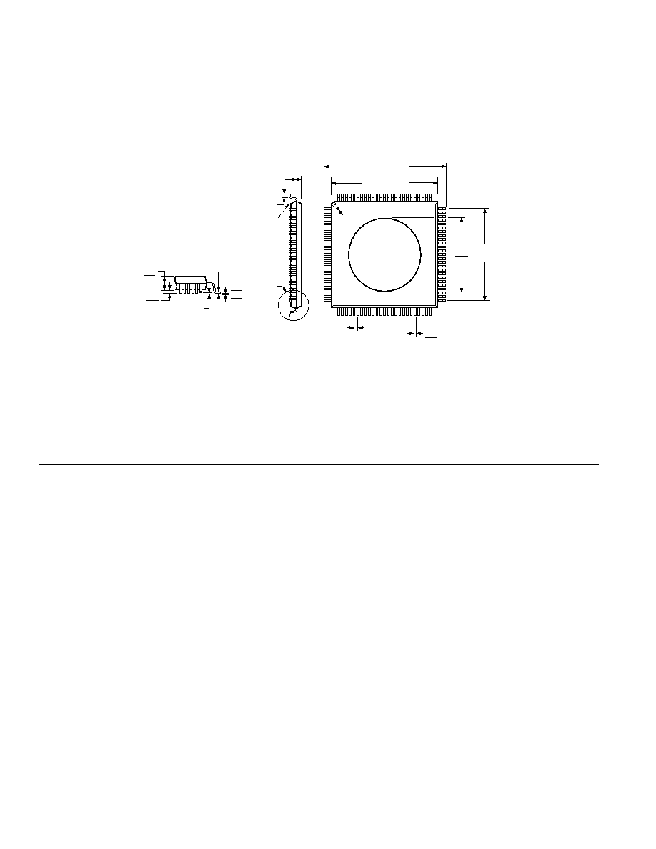
OUTLINE DIMENSIONS
100-Lead Low Profile Quad Flat Package, Integrated Heat Sink [LQFP-ED]
(SQ-100)
Dimensions shown in millimeters
7
3.5
0
VIEW A
ROTATED 90 CCW
0.15
0.05
0.20
0.09
BOTTOM VIEW
(PINS DOWN)
1
25
26
49
76
100
75
50
14.00 BSC SQ
16.00 BSC SQ
12.00
REF
0.27
0.22
0.17
0.50 BSC
VIEW A
1.60 MAX
SEATING
PLANE
0.75
0.60
0.45
1.45
1.40
1.35
COMPLIANT TO JEDEC STANDARDS MS-026BED-HU
0.08
MAX LEAD
COPLANARITY
9.78
9.65
9.40
PIN 1
Revision History
Location
Page
10/03--Data Sheet changed from REV. 0 to REV. A.
Changes to FUNCTIONAL BLOCK DIAGRAM . . . . . . . . . . . . . . . . . . . . . . . . . . . . . . . . . . . . . . . . . . . . . . . . . . . . . . . . . . . . . . 1
Changes to GENERAL DESCRIPTION . . . . . . . . . . . . . . . . . . . . . . . . . . . . . . . . . . . . . . . . . . . . . . . . . . . . . . . . . . . . . . . . . . . . . 1
Changes to SPECIFICATIONS . . . . . . . . . . . . . . . . . . . . . . . . . . . . . . . . . . . . . . . . . . . . . . . . . . . . . . . . . . . . . . . . . . . . . . . . . . . . 2
Changes to PIN FUNCTION DESCRIPTIONS . . . . . . . . . . . . . . . . . . . . . . . . . . . . . . . . . . . . . . . . . . . . . . . . . . . . . . . . . . . . . . . 9
Updated OUTLINE DIMENSIONS . . . . . . . . . . . . . . . . . . . . . . . . . . . . . . . . . . . . . . . . . . . . . . . . . . . . . . . . . . . . . . . . . . . . . . . 12
Document Outline
- FEATURES
- APPLICATIONS
- PRODUCT DESCRIPTION
- FUNCTIONAL BLOCK DIAGRAM
- SPECIFICATIONS
- DRIVER
- COMPARATOR
- ACTIVE LOAD
- DYNAMIC CLAMP
- TOTAL FUNCTION
- POWER SUPPLIES
- ABSOLUTE MAXIMUM RATINGS
- ORDERING GUIDE
- PIN CONFIGURATION
- PIN FUNCTION DESCRIPTIONS
- OUTLINE DIMENSIONS
- Revision History