AD5378 32-Channel, 14-Bit, Parallel and Serial Input, Bipolar Voltage Output DAC Data Sheet (REV. 0)

32-Channel, 14-Bit, Parallel and
Serial Input, Bipolar Voltage Output DAC
AD5378
Rev. 0
Information furnished by Analog Devices is believed to be accurate and reliable.
However, no responsibility is assumed by Analog Devices for its use, nor for any
infringements of patents or other rights of third parties that may result from its use.
Specifications subject to change without notice. No license is granted by implication
or otherwise under any patent or patent rights of Analog Devices. Trademarks and
registered trademarks are the property of their respective owners.
One Technology Way, P.O. Box 9106, Norwood, MA 02062-9106, U.S.A.
Tel: 781.329.4700
www.analog.com
Fax: 781.461.3113
© 2005 Analog Devices, Inc. All rights reserved.
FEATURES
32-channel DAC in 13 mm × 13 mm 108-lead CSPBGA
Guaranteed monotonic to 14 bits
Buffered voltage outputs
Output voltage span of 3.5 V × V
REF
(+)
Maximum output voltage span of 17.5 V
System calibration function allowing user-programmable
offset and gain
Pseudo differential outputs relative to REFGND
Clear function to user-defined REFGND (CLR pin)
Simultaneous update of DAC outputs (LDAC pin)
DAC increment/decrement mode
Channel grouping and addressing features
Interface options
Parallel interface
DSP/microcontroller-compatible 3-wire serial interface
2.5 V to 5.5 V JEDEC-compliant digital levels
SDO daisy-chaining option
Power-on reset
Digital reset (RESET pin and soft reset function)
APPLICATIONS
Level setting in automatic test equipment (ATE)
Variable optical attenuators (VOAs)
Optical switches
Industrial control systems
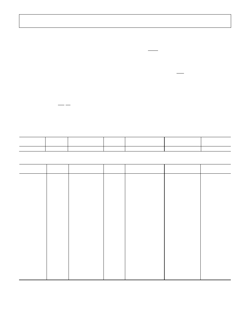
FUNCTIONAL BLOCK DIAGRAM
V
CC
V
DD
V
SS
AGND
RESET
POWER-ON
RESET
DGND
LDAC
V
BIAS
V
REF
1(+) V
REF
1() REFGND A1
VBIAS
DAC 01
DAC
REG
01
DAC
REG
2
DAC
REG
5
DAC
REG
67
INPUT
REG
01
INPUT
REG
2
INPUT
REG
5
INPUT
REG
67
DAC 2
DAC 5
DAC 67
AD5378
DCEN/WR
SYNC/CS
REG0
REG1
DB13
SCLK/DB12
DIN/DB11
DB0
A7
A0
SER/PAR
DIN
SCLK
SDO
FIFOEN
REFGND B1
REFGND B2
REFGND C1
REFGND C2
REFGND D1
REFGND D2
BUSY
V
REF
2(+) V
REF
2() REFGND A2
CLR
VOUT 0
VOUT 1
VOUT 2
VOUT 3
VOUT 4
VOUT 5
VOUT 6
VOUT 7
VOUT 8
VOUT 31
×
4
14
/
14
/
14
/
14
/
14
/
14
/
14
/
14
/
14
/
14
/
14
/
14
/
14
/
14
/
m REG01
c REG01
m REG2
c REG2
m REG7
c REG7
m REG89
c REG89
14
/
14
/
14
/
14
/
14
/
14
/
14
/
S
T
ATE
MACHI
NE
I
N
TE
RFACE
05292-001
Figure 1.
Protected by U.S. Patent No. 5,969,657 and 6,823,416; other patents pending.

AD5378
Rev. 0 | Page 2 of 28
TABLE OF CONTENTS
General Description ..........................................................................3
Specifications......................................................................................4
AC Characteristics........................................................................ 5
Timing Characteristics......................................................................6
Serial Interface .............................................................................. 6
Parallel Interface ........................................................................... 9
Absolute Maximum Ratings...........................................................11
ESD Caution................................................................................ 11
Pin Configuration and Function Descriptions............................12
Typical Performance Characteristics ............................................15
Terminology .....................................................................................17
Functional Description ...................................................................18
DAC Architecture--General..................................................... 18
Channel Groups.......................................................................... 18
Transfer Function ....................................................................... 18
V
BIAS
Function ............................................................................. 19
Reference Selection .................................................................... 19
Calibration................................................................................... 20
Clear Function ............................................................................ 20
BUSY and LDAC Functions...................................................... 20
FIFO vs. Non-FIFO Operation................................................. 21
BUSY Input Function ................................................................ 21
Power-On Reset Function ......................................................... 21
RESET Input Function .............................................................. 21
Increment/Decrement Function .............................................. 21
Interfaces...........................................................................................22
Parallel Interface......................................................................... 22
Serial Interface ............................................................................ 22
Data Decoding .................................................................................24
Address Decoding ...........................................................................25
Power Supply Decoupling ..............................................................26
Power-On .................................................................................... 26
Typical Application Circuit ............................................................27
Outline Dimensions ........................................................................28
Ordering Guide .......................................................................... 28
REVISION HISTORY
4/05--Revision 0: Initial Version
AD5378
Rev. 0 | Page 3 of 28
GENERAL DESCRIPTION
The AD5378 contains 32 14-bit DACs in one CSPBGA package.
The AD5378 provides a bipolar output range determined by the
voltages applied to the V
REF
(+) and V
REF
(-) inputs. The maximum
output voltage span is 17.5 V, corresponding to a bipolar output
range of -8.75 V to +8.75 V, and is achieved with reference volt-
ages of V
REF
(-) = -3.5 V and V
REF
(+) = +5 V.
The AD5378 guarantees operation over a wide V
SS
/V
DD
supply
range from ±11.4 V to ±16.5 V. The output amplifier headroom
requirement is 2.5 V operating with a load current of 1.5 mA,
and 2 V operating with a load current of 0.5 mA.
The AD5378 contains a double-buffered parallel interface in
which 14 data bits are loaded into one of the input registers
under the control of the WR, CS, and DAC channel address
pins, A0 to A7. It also has a 3-wire serial interface, which is
compatible with SPI®, QSPITM, MICROWIRETM, and DSP inter-
face standards and can handle clock speeds of up to 50 MHz.
The DAC outputs are updated when the DAC registers receive
new data. All the outputs can be updated simultaneously by
taking the LDAC input low. Each channel has a programmable
gain and an offset adjust register.
Each DAC output is gained and buffered on-chip with respect
to an external REFGND input. The DAC outputs can also be
switched to REFGND via the CLR pin. Table 1 and Table 2
show the product portfolio for high channel count bipolar and
unipolar voltage output DACs.
Table 1. 40-Channel, Bipolar, Voltage Output DAC
Model Resolution
Analog
Supplies
Output
Channels Linearity
Error
(LSB)
Package
Description Package
Option
AD5379ABC
14 Bits
±11.4 V to ±16.5 V
40
±3
108-Lead CSPBGA
BC-108
Table 2. High Channel Count, Low Voltage, Single-Supply DACs
Model Resolution
AV
DD
Range
Output
Channels
Linearity Error (LSB)
Package
Description
Package Option
AD5380BST-5
14 Bits
4.5 V to 5.5 V
40
±4
100-Lead LQFP
ST-100
AD5380BST-3
14 Bits
2.7 V to 3.6 V
40
±4
100-Lead LQFP
ST-100
AD5381BST-5
12 Bits
4.5 V to 5.5 V
40
±1
100-Lead LQFP
ST-100
AD5381BST-3
12 Bits
2.7 V to 3.6 V
40
±1
100-Lead LQFP
ST-100
AD5384BBC-5
14 Bits
4.5 V to 5.5 V
40
±4
100-Lead CSPBGA
BC-100
AD5384BBC-3
14 Bits
2.7 V to 3.6 V
40
±4
100-Lead CSPBGA
BC-100
AD5382BST-5
14 Bits
4.5 V to 5.5 V
32
±4
100-Lead LQFP
ST-100
AD5382BST-3
14 Bits
2.7 V to 3.6 V
32
±4
100-Lead LQFP
ST-100
AD5383BST-5
12 Bits
4.5 V to 5.5 V
32
±1
100-Lead LQFP
ST-100
AD5383BST-3
12 Bits
2.7 V to 3.6 V
32
±1
100-Lead LQFP
ST-100
AD5390BST-5
14 Bits
4.5 V to 5.5 V
16
±3
52-Lead LQFP
ST-52
AD5390BCP-5
14 Bits
4.5 V to 5.5 V
16
±3
64-Lead LFCSP
CP-64
AD5390BST-3
14 Bits
2.7 V to 3.6 V
16
±4
52-Lead LQFP
ST-52
AD5390BCP-3
14 Bits
2.7 V to 3.6 V
16
±4
64-Lead LFCSP
CP-64
AD5391BST-5
12 Bits
4.5 V to 5.5 V
16
±1
52-Lead LQFP
ST-52
AD5391BCP-5
12 Bits
4.5 V to 5.5 V
16
±1
64-Lead LFCSP
CP-64
AD5391BST-3
12 Bits
2.7 V to 3.6 V
16
±1
52-Lead LQFP
ST-52
AD5391BCP-3
12 Bits
2.7 V to 3.6 V
16
±1
64-Lead LFCSP
CP-64
AD5392BST-5
14 Bits
4.5 V to 5.5 V
8
±3
52-Lead LQFP
ST-52
AD5392BCP-5
14 Bits
4.5 V to 5.5 V
8
±3
64-Lead LFCSP
CP-64
AD5392BST-3
14 Bits
2.7 V to 3.6 V
8
±4
52-Lead LQFP
ST-52
AD5392BCP-3
14 Bits
2.7 V to 3.6 V
8
±4
64-Lead LFCSP
CP-64

AD5378
Rev. 0 | Page 4 of 28
SPECIFICATIONS
V
CC
= 2.7 V to 5.5 V; V
DD
= 11.4 V to 16.5 V; V
SS
= -11.4 V to -16.5 V; V
REF
(+) = +5 V; V
REF
(-) = -3.5 V; AGND = DGND = REFGND =
0 V; V
BIAS
= 5 V; C
L
= 200 pF to GND; R
L
= 11 k to 3 V; gain = 1; offset = 0 V; all specifications T
MIN
to T
MAX
, unless otherwise noted.
Table 3.
Parameter A
Version
1
Unit Test
Conditions/Comments
ACCURACY
Resolution 14
Bits
Relative Accuracy
±3
LSB max
-40°C to +85°C
±2.5
LSB max
0°C to 70°C
Differential Nonlinearity
-1/+1.5
LSB max
Guaranteed monotonic by design over temperature
Zero-Scale Error
±12
mV max
-40°C to +85°C
±5
mV max
0°C to 70°C
Full-Scale Error
±12
mV max
-40°C to +85°C
±8
mV max
0°C to 70°C
Gain Error
±8
mV max
-40°C to +85°C
±1/±5
mV typ/max
0°C to 70°C
VOUT Temperature Coefficient
5
ppm FSR/°C typ
Includes linearity, offset, and gain drift; see Figure 11
DC Crosstalk
2
0.5
mV max
Typically 100 µV
REFERENCE INPUTS
2
V
REF
(+) DC Input Impedance
1
M min
Typically 100 M
V
REF
(-) DC Input Impedance
8
k min
Typically 12 k
V
REF
(+) Input Current
±10
µA max
Per input; typically ±30 nA
V
REF
(+) Range
1.5/5
V min/max
±2% for specified operation
V
REF
(-) Range
-3.5/0
V min/max
±2% for specified operation
REFGND INPUTS
2
DC Input Impedance
80
k min
Typically 120 k
Input Range
±0.5
V min/max
OUTPUT CHARACTERISTICS
2
Output Voltage Range
V
SS
+ 2/V
SS
+ 2.5
V min
I
LOAD
= ±0.5 mA/±1.5 mA
V
DD
- 2/V
DD
- 2.5
V max
I
LOAD
= ±0.5 mA/±1.5 mA
Short-Circuit Current
15
mA max
Load Current
±1.5
mA max
Capacitive Load
2200
pF max
DC Output Impedance
1
max
DIGITAL INPUTS
JEDEC-compliant
Input High Voltage
1.7
V min
V
CC
= 2.7 V to 3.6 V
2.0
V
min
V
CC
= 3.6 V to 5.5 V
Input Low Voltage
0.8
V max
V
CC
= 2.7 V to 5.5 V
Input Current (with pull-up/pull-down)
±8
µA max
SER/PAR, FIFOEN, and RESET pins only
Input Current (no pull-up/pull-down)
±1
µA max
All other digital input pins
Input Capacitance
2
10
pF
max
DIGITAL OUTPUTS (BUSY, SDO)
Output Low Voltage
0.5
V max
Sinking 200 µA
Output High Voltage (SDO)
V
CC
- 0.5
V min
Sourcing 200 µA
High Impedance Leakage Current
-70
µA max
SDO only
High Impedance Output Capacitance
2
10
pF
typ
AD5378
Rev. 0 | Page 5 of 28
Parameter A
Version
1
Unit Test
Conditions/Comments
POWER REQUIREMENTS
V
CC
2.7/5.5 V
min/max
V
DD
8.5/16.5 V
min/max
V
SS
-3/-16.5 V
min/max
Power Supply Sensitivity
2
Full Scale/ V
DD
-75 dB
typ
Full Scale/ V
SS
-75 dB
typ
Full Scale/ V
CC
-90 dB
typ
I
CC
5 mA
max
V
CC
= 5.5 V, V
IH
= V
CC
, V
IL
= GND
I
DD
28
mA max
Outputs unloaded; typically 20 mA
I
SS
23
mA max
Outputs unloaded; typically 15 mA
Power Dissipation
Power Dissipation Unloaded (P)
850
mW max
V
DD
= 16.5 V, V
SS
= -16.5 V
Power Dissipation Loaded (P
TOTAL
) 2000
mW
max
P
TOTAL
= P + (V
DD
- V
O
) × I
SOURCE
+ (V
O
- V
SS
) × I
SINK
Junction Temperature
130
°C max
T
J
= T
A
+ P
TOTAL
×
J
3
1
Temperature range for the A version: -40°C to +85°C. Typical specifications are at 25°C.
2
Guaranteed by design and characterization; not production tested.
3
Where
J
represents the package thermal impedance.
AC CHARACTERISTICS
V
CC
= 2.7 V to 5.5 V; V
DD
= 11.4 V to 16.5 V; V
SS
= -11.4 V to -16.5 V; V
REF
(+) = +5 V; V
REF
(-) = -3.5 V;
AGND = DGND = REFGND = 0 V; V
BIAS
= 5 V; C
L
= 220 pF; R
L
= 11 k to 3 V; gain = 1; offset = 0 V.
Table 4.
Parameter A
Version
1
Unit Test
Conditions/Comments
DYNAMIC PERFORMANCE
Output Voltage Settling Time
20
µs typ
Full-scale change to ±1/2 LSB
30
µs max
DAC latch contents alternately loaded with all 0s and
all 1s
Slew Rate
1
V/µs typ
Digital-to-Analog Glitch Energy
20
nV-s typ
Glitch Impulse Peak Amplitude
15
mV max
Channel-to-Channel Isolation
100
dB typ
V
REF
(+) = 2 V p-p, (1 V
BIAS
) 1 kHz, V
REF
(-) = -1 V
DAC-to-DAC Crosstalk
40
nV-s typ
See the Terminology section; between DACs inside a
group
10
nV-s typ
Between DACs from different groups
Digital Crosstalk
0.1
nV-s typ
Digital Feedthrough
1
nV-s typ
Effect of input bus activity on DAC output under test
Output Noise Spectral Density @ 1 kHz
350
nV/(Hz)
1/2
typ
V
REF
(+) = V
REF
(-) = 0 V
1
Guaranteed by design and characterization; not production tested.
Document Outline