AD5398 120 mA, Current Sinking, 10-Bit, I2C DAC Data Sheet (REV. 0)
120 mA, Current Sinking, 10-Bit, I
2
C DAC
AD5398
5
Rev. 0
Information furnished by Analog Devices is believed to be accurate and reliable.
However, no responsibility is assumed by Analog Devices for its use, nor for any
infringements of patents or other rights of third parties that may result from its use.
Specifications subject to change without notice. No license is granted by implication
or otherwise under any patent or patent rights of Analog Devices. Trademarks and
registered trademarks are the property of their respective owners.
One Technology Way, P.O. Box 9106, Norwood, MA 02062-9106, U.S.A.
Tel: 781.329.4700
www.analog.com
Fax: 781.326.8703
© 2004 Analog Devices, Inc. All rights reserved.
FEATURES
120 mA current sink
Available in 8-lead LFCSP package
2-wire (I
2
C®-compatible) serial interface
10-bit resolution
Integrated current sense resistor
2.7 V to 5.5 V power supply
Guaranteed monotonic over all codes
Power-down to 0.5 µA typical
Internal reference
Ultralow noise preamplifier
Power-down function
Power-on reset
CONSUMER/COMMUNICATIONS APPLICATIONS
Lens autofocus
Image stabilization
Optical zoom
Shutters
Iris/exposure
Neutral density filter NDFs
Lens covers
Camera phones
Digital still cameras
Camera modules
Digital video cameras (DVCs)/camcorders
Camera-enabled devices
Security cameras
Web/PC cameras
INDUSTRIAL APPLICATIONS
Heater control
Fan control
Cooler (Peltier) control
Solenoid control
Valve control
Linear actuator control
Light control
Current loop control
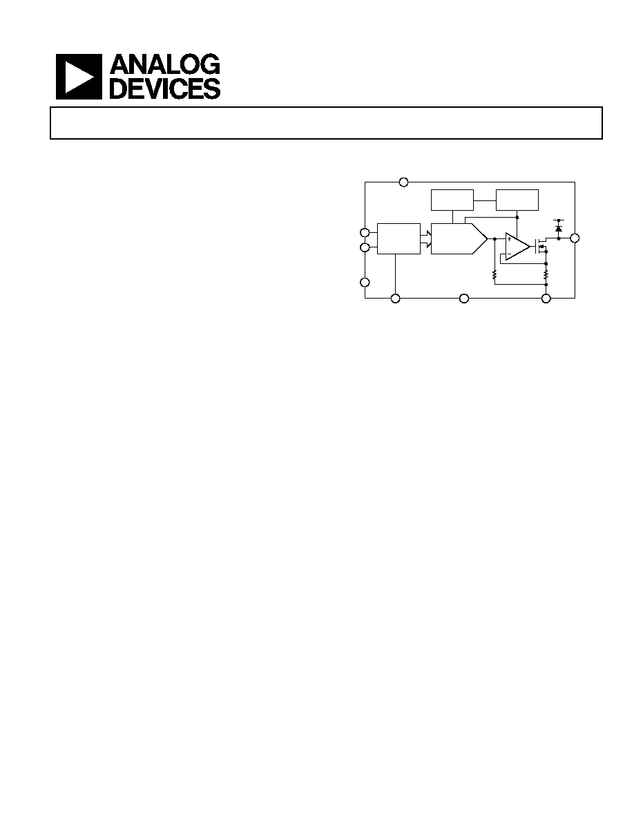
FUNCTIONAL BLOCK DIAGRAM
05034-001
POWER-ON
RESET
3
SDA
7
AGND
2
DGND
6
V
DD
4
SCL
1
PD
8
I
SINK
R
SENSE
3.3
I
2
C SERIAL
INTERFACE
10-BIT
CURRENT
OUTPUT DAC
REFERENCE
R
AD5398
5
DGND
Figure 1.
GENERAL DESCRIPTION
The AD5398 is a single 10-bit DAC with 120 mA output
current sink capability. It features an internal reference, and
operates from a single 2.7 V to 5.5 V supply. The DAC is
controlled via a 2-wire (I
2
C-compatible) serial interface that
operates at clock rates up to 400 kHz.
The AD5398 incorporates a power-on reset circuit, which
ensures that the DAC output powers up to 0 V and remains
there until a valid write takes place. It has a power-down
feature that reduces the current consumption of the device to
1 µA max.
The AD5398 is designed for autofocus, image stabilization,
and optical zoom applications in camera phones, digital still
cameras, and camcorders.
The AD5398 also has many industrial applications, such as
controlling temperature, light, and movement, over the range
-
40°C to +85°C without derating.
The I
2
C address range for the AD5398 is 0x18 to 0x1F
inclusive.

AD5398
Rev. 0 | Page 2 of 16
TABLE OF CONTENTS
Specifications..................................................................................... 3
AC Characteristics............................................................................ 4
Timing Characteristics..................................................................... 4
Absolute Maximum Ratings............................................................ 5
ESD Caution.................................................................................. 5
Pin Configuration and Function Descriptions............................. 6
Typical Performance Characteristics ............................................. 7
Terminology ...................................................................................... 9
Theory of Operation ...................................................................... 10
Serial Interface ............................................................................ 10
I
2
C Bus Operation ...................................................................... 10
Data Format ................................................................................ 10
Power Supply Bypassing and Grounding................................ 11
Applications..................................................................................... 13
Outline Dimensions ....................................................................... 14
Ordering Guide .......................................................................... 14
REVISION HISTORY
12/04--Revision 0: Initial Version

AD5398
Rev. 0 | Page 3 of 16
SPECIFICATIONS
V
DD
= 2.7 V to 5.5 V, AGND = DGND = 0 V, load resistance R
L
= 25 connected to V
DD
; all specifications T
MIN
to T
MAX
,
unless otherwise noted.
Table 1.
B
Version
1
Parameter Min
Typ
Max
Unit
Test
Conditions/Comments
DC
PERFORMANCE
V
DD
= 3.6 V to 4.5 V. Device operates over 2.7 V to 5.5 V
with reduced performance.
Resolution
10
Bits
117
µA/LSB
Relative Accuracy
2
±1.5
±4
LSB
Differential Nonlinearity
2, 3
±1
LSB
Guaranteed monotonic over all codes.
Zero Code Error
2, 4
0 1 5 mA
All
0s
loaded
to
DAC.
Offset Error @ Code 16
2
0.5
mA
Gain Error
2
±0.6
% of FSR
@ 25°C
Offset Error Drift
4, 5
10
µA/ºC
Gain Error Drift
2, 5
±0.2 ±0.5 LSB/ºC
OUTPUT
CHARACTERISTICS
Minimum Sink Current
4
3
mA
Maximum Sink Current
120
mA
V
DD
= 3.6 V to 4.5 V. Device operates over 2.7 V to 5.5 V, but
specified maximum sink current might not be achieved.
Output Current During PD
80
nA
PD = 1.
Output Compliance
5
0.6
V
DD
V
Output voltage range over which max sink current is
available.
Power-Up Time
20
µs
To 10% of FS, coming out of power-down mode. V
DD
= 5 V.
LOGIC INPUTS (PD)
5
Input
Current
±1
µA
Input Low Voltage, V
INL
0.8
V V
DD
= 2.7 V to 5.5 V
Input High Voltage, V
INH
0.7 V
DD
V
V
DD
= 2.7 V to 5.5 V
Pin
Capacitance
3
pF
LOGIC INPUTS (SCL, SDA)
5
Input Low Voltage, V
INL
-0.3
0.3
V
DD
V
Input High Voltage, V
INH
0.7 V
DD
V
DD
+ 0.3
V
Input Leakage Current I
IN
±1
µA
V
IN
= 0 V to V
DD
Input Hysteresis, V
HYST
0.05 V
DD
V
Digital Input Capacitance, C
IN
6
pF
Glitch Rejection
6
50
ns
Pulse width of spike suppressed.
POWER
REQUIREMENTS
V
DD
2.7
5.5 V
I
DD
(Normal
Mode)
I
DD
specification is valid for all DAC codes.
V
DD
= 2.7 V to 5.5 V
V
DD
= 2.7 V to 4.5 V
2.5
2.3
4
3
mA
mA
V
IH
= V
DD
, and V
IL
= GND, V
DD
= 5.5 V
V
IH
= V
DD
, and V
IL
= GND, V
DD
= 4.5 V
I
DD
(Power-Down Mode)
0.5
1
µA
V
IH
= V
DD
, and V
IL
= GND
1
Temperature range is as follows: B Version: 40°C to +85°C.
2
See the Terminology section.
3
Linearity is tested using a reduced code range: Codes 32 to 1023.
4
To achieve near zero output current, use the power-down feature.
5
Guaranteed by design and characterization; not production tested.
6
Input filtering on both the SCL and SDA inputs suppresses noise spikes that are less than 50 ns.
AD5398
Rev. 0 | Page 4 of 16
AC CHARACTERISTICS
V
DD
= 2.7 V to 5.5 V, AGND = DGND = 0 V, load resistance R
L
= 25 connected to V
DD
, unless otherwise noted.
Table 2.
B
Version
1, 2
Parameter Min
Typ
Max
Unit
Test
Conditions/Comments
Output Current Settling Time
250
µs
V
DD
= 5 V, R
L
= 25 , L
L
= 680 µH
¼ scale to ¾ scale change (0x100 to 0x300)
Slew Rate
0.3
mA/µs
Major Code Change Glitch Impulse
0.15
nA-s
1 LSB change around major carry
Digital Feedthrough
3
0.06
nA-s
1
Temperature range is as follows: B Version: 40°C to +85°C.
2
Guaranteed by design and characterization; not production tested.
3
See the
section.
Terminology
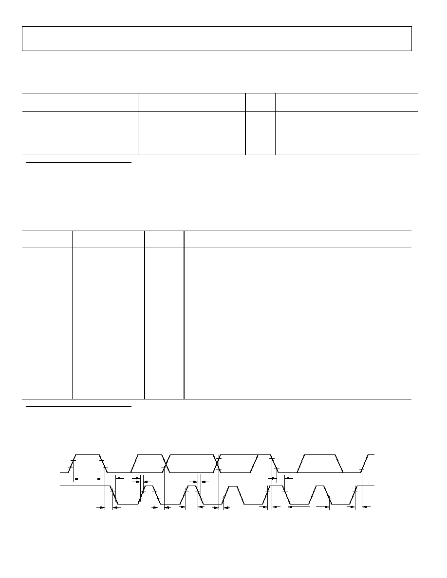
TIMING CHARACTERISTICS
V
DD
= 2.7 V to 5.5 V. All specifications T
MIN
to T
MAX
, unless otherwise noted.
Table 3.
Parameter
1
Limit at T
MIN
, T
MAX
(B Version)
Unit
Conditions/Comments
f
SCL
400
kHz max
SCL clock frequency
t
1
2.5
µs min
SCL cycle time
t
2
0.6 µs
min
t
HIGH
, SCL high time
t
3
1.3 µs
min
t
LOW
, SCL low time
t
4
0.6 µs
min
t
HD,STA
, start/repeated start condition hold time
t
5
100 ns
min
t
SU,DAT
, data setup time
t
6
2
0.9 µs
max
t
HD,DAT
, data hold time
0
µs
min
t
7
0.6 µs
min
t
SU,STA
, setup time for repeated start
t
8
0.6 µs
min
t
SU,STO
, stop condition setup time
t
9
1.3 µs
min
t
BUF
, bus free time between a stop condition and a start condition
t
10
300 ns
max
t
R,
rise time of both SCL and SDA when receiving
0
ns min
May be CMOS driven
t
11
250 ns
max
t
F
, fall time of SDA when receiving
300
ns
max
t
F
, fall time of Both SCL and SDA when transmitting
20 + 0.1 C
b
3
ns min
C
b
400
pF max
Capacitive load for each bus line
1
Guaranteed by design and characterization; not production tested.
2
A master device must provide a hold time of at least 300 ns for the SDA signal (referred to the V
IH MIN
of the SCL signal) in order to bridge the undefined region of SCL's
falling edge.
3
C
b
is the total capacitance of one bus line in pF. t
R
and t
F
are measured between 0.3 V
DD
and 0.7 V
DD.
05034-
002
SDA
t
9
SCL
t
3
t
10
t
11
t
4
t
4
t
6
t
2
t
5
t
7
t
1
t
8
START
CONDITION
REPEATED
START
CONDITION
STOP
CONDITION
Figure 2. 2-Wire Serial Interface Timing Diagram
AD5398
Rev. 0 | Page 5 of 16
ABSOLUTE MAXIMUM RATINGS
T
A
= 25°C, unless otherwise noted.
1
Table 4.
Parameter
Rating
V
DD
to AGND
0.3 V to +7 V
V
DD
to DGND
0.3 V to V
DD
+ 0.3 V
AGND to DGND
0.3 V to +0.3 V
SCL, SDA to DGND
0.3 V to V
DD
+ 0.3 V
PD to DGND
0.3 V to V
DD
+ 0.3 V
I
SINK
to AGND
0.3 V to V
DD
+ 0.3 V
Operating Temperature Range
Industrial (B Version)
40°C to +85°C
Storage Temperature Range
65°C to +150°C
Junction Temperature (T
J
max)
150°C
LFCSP Power Dissipation
(T
J
max T
A
)/
JA
JA
Thermal Impedance
2
Mounted on 2-Layer Board
84°C/W
Mounted on 4-Layer Board
48°C/W
Lead Temperature, Soldering
Vapor Phase (60 sec)
215°C
Infrared (15 sec)
220°C
____________________
1
Transient currents of up to 100 mA do not cause SCR latch-up.
2
To achieve the optimum
JA
, it is recommended that the AD5398 is soldered on a
4-layer board. The AD5398 comes in an 8-lead LFCSP package with an exposed
paddle that should be connected to the same potential as the AD5398 DGND pin.
Stresses above those listed under Absolute Maximum Ratings
may cause permanent damage to the device. This is a stress
rating only; functional operation of the device at these or any
other conditions above those listed in the operational sections
of this specification is not implied. Exposure to absolute
maximum rating conditions for extended periods may affect
device reliability. Only one absolute maximum rating may be
applied at any one time.
ESD CAUTION
ESD (electrostatic discharge) sensitive device. Electrostatic charges as high as 4000 V readily accumulate on
the human body and test equipment and can discharge without detection. Although this product features
proprietary ESD protection circuitry, permanent damage may occur on devices subjected to high energy
electrostatic discharges. Therefore, proper ESD precautions are recommended to avoid performance
degradation or loss of functionality.
Document Outline
- FEATURES
- CONSUMER/COMMUNICATIONS APPLICATIONS
- INDUSTRIAL APPLICATIONS
- FUNCTIONAL BLOCK DIAGRAM
- GENERAL DESCRIPTION
- þÿ
- þÿ
- þÿ
- þÿ
- þÿ
- þÿ
- þÿ
- þÿ
- þÿ
- þÿ