 | ÐлекÑÑоннÑй компоненÑ: AD5399YRM | СкаÑаÑÑ:  PDF PDF  ZIP ZIP |
Äîêóìåíòàöèÿ è îïèñàíèÿ www.docs.chipfind.ru
Twos Complement, Dual 12-Bit DAC
with Internal REF and Fast Settling Time
AD5399
Rev. D
Information furnished by Analog Devices is believed to be accurate and reliable.
However, no responsibility is assumed by Analog Devices for its use, nor for any
infringements of patents or other rights of third parties that may result from its use.
Specifications subject to change without notice. No license is granted by implication
or otherwise under any patent or patent rights of Analog Devices. Trademarks and
registered trademarks are the property of their respective owners.
One Technology Way, P.O. Box 9106, Norwood, MA 02062-9106, U.S.A.
Tel: 781.329.4700
www.analog.com
Fax: 781.326.8703
© 2004 Analog Devices, Inc. All rights reserved.
FEATURES
2-channel 12-bit DAC
Twos complement facilitates bipolar applications
Bipolar zero with 2 V dc offset
Built-in 2.000 V precision reference with 10 ppm/°C typ TC
Buffered voltage output: 0 V to 4 V
Single-supply operation: 4.5 V to 5.5 V
Fast 0.8 µs settling time typ
Ultracompact MSOP-10 package
Monotonic DNL < ±1 LSB
Optimized accuracy at zero scale
Power-on reset to V
REF
3-wire serial data input
Extended temperature range: 40°C to +105°C
APPLICATIONS
Single-supply bipolar converter operations
General-purpose DSP applications
Digital gain and offset controls
Instrumentation level settings
Disk drive control
Precision motor control
GENERAL DESCRIPTION
The AD5399 is the industry-first dual 12-bit digital-to-analog
converter that accepts twos complement digital coding with 2 V
dc offset for single-supply operation. Augmented with a built-in
precision reference and a solid buffer amplifier, the AD5399 is
the smallest self-contained 12-bit precision DAC that fits many
general-purpose as well as DSP specific applications. The twos
complement programming facilitates the natural coding
implementation commonly found in DSP applications, and
allows operation in single supply. The AD5399 provides a 2 V
reference output, V
REF
, for bipolar zero monitoring. It can also
be used for other on-board components that require a precision
reference. The device is specified for operation from 5 V ± 10%
single supply with bipolar output swing from 0 V to 4 V
centered at 2 V.
The AD5399 is available in the compact 1.1 mm low profile
MSOP-10 package. All parts are guaranteed to operate over the
extended industrial temperature range of 40°C to +105°C.
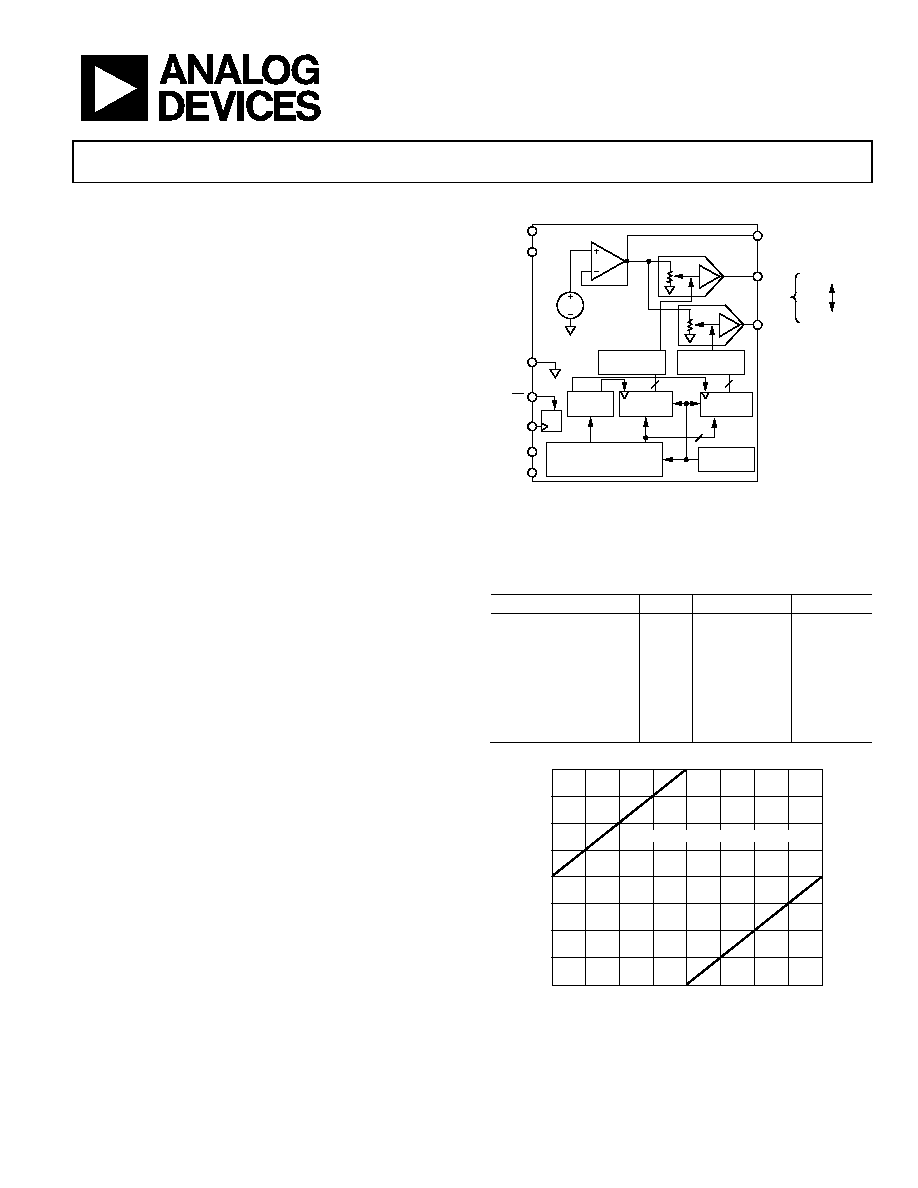
FUNCTIONAL BLOCK DIAGRAM
X2
×2
V
REF
2V
×2
DECODER SW
DRIVER A
DECODER SW
DRIVER B
ADDR
DECODE
DAC A
REGISTER
DAC B
REGISTER
16-BIT
D15...D0
POWER-ON
RESET
EN
A0
12
12
12
CLK
CS
SDI
DGND
AGND
V
TP
V
DD
V
BZ
+ 2V = 4V
V
BZ
2V = 0V
V
OUTA
V
OUTB
V
BZ
(V
REF
) = 2V
AD5399
03469-B-001
Figure 1.
V
OUT
= ((D 2048)/4096 × 4 V) + 2 V for 0 D 4095, where D
is the decimal code.
Table 1. Examples of Twos Complement Codes
Twos Complement
D
Scale
V
OUT
(V)
2047 4095
+FS
4.000
2046
4094
+FS 1 LSB
3.999
1
2049
BZS + 1 LSB
2.001
0 2048
BZS
2.000
4095
2047
BZS 1 LSB
1.999
2049
1
FS + 1 LSB
0.001
2048 0
FS
0.000
FS = Full Scale, BZS = Bipolar Zero Scale.
V
OUT
= [(0 2048)/4096 × 4V] + 2V
0
1.0
0.5
3.0
3.5
2.0
1.5
2.5
4.0
0
512
1024
1536
2048
2560
3072
3584
4096
TWOS COMPLEMENT CODE
V
OUT
(V
)
03469-B
-
002
Figure 2. Output vs. Twos Complement Code

AD5399
Rev. D | Page 2 of 12
TABLE OF CONTENTS
Specifications..................................................................................... 3
Electrical Characteristics ............................................................. 3
Absolute Maximum Ratings............................................................ 4
ESD Caution.................................................................................. 4
Pin Configuration and Function Descriptions............................. 5
Timing Characteristics..................................................................... 6
Typical Performance Characteristics ..............................................7
Operation......................................................................................... 10
Power-Up/Power-Down Sequence .......................................... 10
Outline Dimensions ....................................................................... 12
Ordering Guide .......................................................................... 12
REVISION HISTORY
6/04--Data sheet changed from Rev. C to Rev. D
Correction to Table 7 Caption ...................................................... 11
3/04--Data sheet changed from Rev. B to Rev. C
Changes to Specifications ................................................................ 3
Changes to Table 4............................................................................ 5
Replaced Figures 4 and 5 ................................................................. 6
Changes to Operation Section ...................................................... 10
Changes to Table 6.......................................................................... 10
11/03--Data sheet changed from Rev. A to Rev. B
Changes to Table 5 notes ................................................................. 5
Changes to Figures 8 and 9.............................................................. 7
Changes to Figure 12........................................................................ 8
Added Power-Up/Power-Down section ...................................... 10
3/03--Data sheet changed from Rev. 0 to Rev. A
Change to Table 1 ............................................................................. 1
2/03--Revision 0: Initial Version

AD5399
Rev. D | Page 3 of 12
SPECIFICATIONS
ELECTRICAL CHARACTERISTICS
V
DD
= 5 V ± 10%, 40°C < T
A
< +105°C, unless otherwise noted.
Table 2.
Parameter Symbol
Conditions
Min
Typ
1
Max Unit
DC
CHARACTERISTICS
Resolution
N
12
Bits
Differential Nonlinearity Error
DNL
1
±0.5
+1
LSB
Codes 2048 to 2052, due to int. op amp offset
1.2
±0.5
+1.2
LSB
Integral Nonlinearity Error
INL
0.4
±0.02
+0.4
%FS
Positive Full-Scale Error
V
+FSE
Code = 0xF
0.75
0.15
+0.75
%FS
Bipolar Zero-Scale Error
V
BZSE
Code = 0x000
0.75
0.15
+0.75
%FS
Negative Full-Scale Error
V
FSE
Code = 0x800
0.75
0.15
+0.75
%FS
ANALOG
OUTPUTS
Nominal Positive Full-Scale
V
OUTA/B
Code = 0x7FF
4
V
Positive Full-Scale Tempco
2
TCV
OUTA/B
Code = 0x7FF, T
A
= 0°C to 70°C
40
±10
+40
ppm/°C
Code = 0xFF, T
A
= 40°C to +105°C
60
±10
+60
ppm/°C
Nominal V
BZ
Output Voltage
V
BZ
1.995 2.000 2.004 V
Bipolar Zero Output Resistance
2
R
BZ
1
V
BZ
Output Voltage Tempco
TCV
BZ
T
A
= 0°C to 70°C
40
±10
+40
ppm/°C
T
A
= 40°C to +105°C
60
±10
+60
ppm/°C
Nominal Peak-to-Peak Output Swing
|V
+FS
| + |V
FS
|
Code 0x7FF to Code 0x800
4
V
DIGITAL
INPUTS
Input Logic High
V
IH
V
DD
= 5 V
2.4
V
Input Logic Low
V
IL
V
DD
= 5 V
0.8
V
Input Current
I
IL
V
IN
= 0 V or 5 V, V
DD
= 5 V
±1
µA
Input Capacitance
2
C
IL
5
pF
POWER
SUPPLIES
Power Supply Range
V
DD RANGE
4.5
5.5 V
Supply Current
I
DD
V
IH
= V
DD
or V
IL
= 0 V
1.8
2.6
mA
Supply Current in Shutdown
I
DD_SHDN
V
IH
= V
DD
or V
IL
= 0 V, B14 = 0, T
A
= 0°C to 105°C
10
100
µA
V
IH
= V
DD
or V
IL
= 0 V, B14 = 0, T
A
= 40°C to 0°C
100
500
µA
Power Dissipation
3
P
DISS
V
IH
= V
DD
or V
IL
= 0 V, V
DD
= 5.5 V
9
13
mW
Power Supply Sensitivity
P
SS
V
DD
= 5 V ± 10%
0.006
+0.003
+0.006
%/%
DYNAMIC CHARACTERISTICS
2
Settling Time
t
S
0.1% error band
0.8
µs
Digital Feedthrough
Q
10
nV-s
Bipolar Zero-Scale Glitch
G
10
nV-s
Capacitive Load Driving Capability CL
No
oscillation
1000
pF
INTERFACE TIMING CHARACTERISTICS
2
, 4
SCLK Cycle Frequency
t
CYC
33
MHz
SCLK Clock Cycle Time
t
1
30
ns
Input Clock Pulse Width
t
2
, t
3
Clock level low or high
15
ns
Data Setup Time
t
4
5
ns
Data Hold Time
t
5
0
ns
CS to SCLK Active Edge Setup Time
t
6
5
ns
SCLK to CS Hold Time
t
7
0
ns
Repeat Programming, CS High Time
t
8
30
ns
1
Typical values represent average readings at 25°C and V
DD
= 5 V.
2
Guaranteed by design and not subject to production test.
3
P
DISS
is calculated from (I
DD
× V
DD
). CMOS logic level inputs result in minimum power dissipation.
4
See timing diagram (Figure 5) for location of measured values. All input control voltages are specified with t
R
= t
F
= 2 ns (10% to 90% of 3 V) and timed from a voltage
level of 1.5 V. Switching characteristics are measured using V
DD
= 5 V. Input logic should have a 1 V/µs minimum slew rate.
AD5399
Rev. D | Page 4 of 12
ABSOLUTE MAXIMUM RATINGS
T
A
= 25°C, unless otherwise noted.
Table 3.
Parameter Rating
V
DD
to GND
0.3 V, +7.5 V
V
OUTA
, V
OUTB
, V
BZ
to GND
0 V, V
DD
Digital Input Voltages to GND
0 V, V
DD
+ 0.3 V
Operating Temperature Range
40°C to +105°C
Maximum Junction Temperature (T
J
MAX
) 150°C
Storage Temperature
65°C to +150°C
Lead Temperature (Soldering, 10 sec)
300°C
Package Power Dissipation
(T
J MAX
T
A
)/
JA
Thermal Resistance,
JA
, MSOP-10
206°C/W
Stresses above those listed under Absolute Maximum Ratings
may cause permanent damage to the device. This is a stress
rating only; functional operation of the device at these or any
other conditions above those indicated in the operational
section of this specification is not implied. Exposure to absolute
maximum rating conditions for extended periods may affect
device reliability.
ESD CAUTION
ESD (electrostatic discharge) sensitive device. Electrostatic charges as high as 4000 V readily accumulate on
the human body and test equipment and can discharge without detection. Although this product features
proprietary ESD protection circuitry, permanent damage may occur on devices subjected to high energy
electrostatic discharges. Therefore, proper ESD precautions are recommended to avoid performance
degradation or loss of functionality.
AD5399
Rev. D | Page 5 of 12
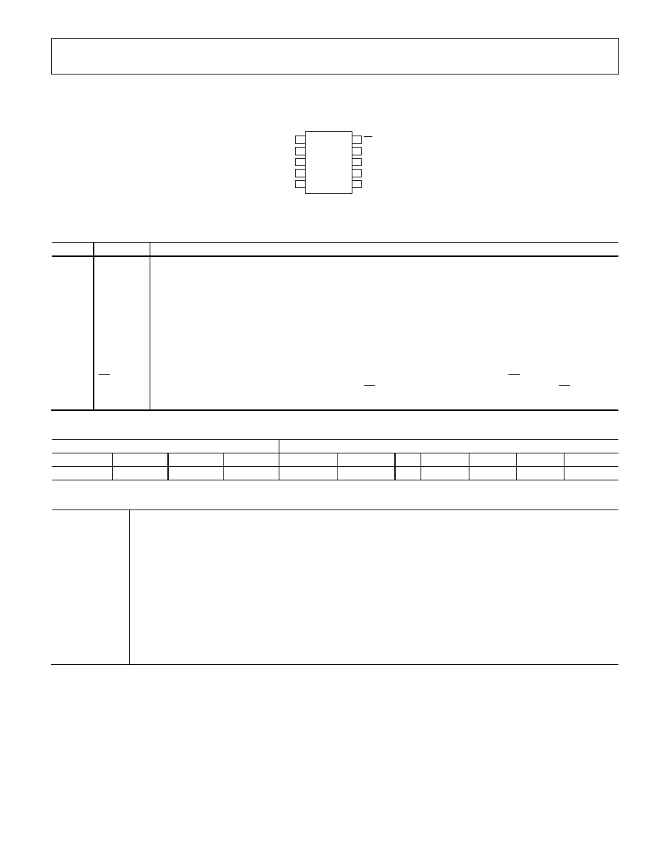
PIN CONFIGURATION AND FUNCTION DESCRIPTIONS
AD5399
TOP VIEW
(Not to Scale)
CLK
1
SDI
2
DGND
3
V
OUTB
4
V
OUTA
5
CS
V
TP
V
DD
AGND
V
BZ
10
9
8
7
6
03469-B
-
003
Figure 3. MSOP-10 Pin Configuration
Table 4. Pin Function Descriptions
Pin No.
Mnemonic
Description
1
CLK
Serial Clock Input. Positive edge triggered.
2
SDI
Serial Data Input. MSB first format.
3 DGND
Digital
Ground.
4 V
OUTB
DAC B Voltage Output (A0 = Logic 1).
5 V
OUTA
DAC A Voltage Output (A0 = Logic 0).
6 V
BZ
2 V, Virtual Bipolar Zero (Active Output).
7 AGND
Analog
Ground.
8 V
DD
Positive Power Supply. Specified for operation at 5 V.
9 V
TP
Connect to V
DD
. Reserved for factory testing.
10
CS
Chip Select (Frame Sync Input). Allows clock and data to shift into the shift register when CS goes from high to low.
After the 16
th
clock pulse, it is not necessary to bring CS high to shift the data to the output. However, CS should be
brought high any time after the 16th clock positive edge in order to allow the next programming cycle.
Table 5. Serial Data-Word Format
ADDR DATA
B15 B14 B13 B12 B11 B10
...
B3 B2 B1 B0
A0
X
SD 0
D11 D10 ...
D3 D2 D1 D0
MSB
LSB
A0
Address Bit. Logic low selects DAC A and logic high selects DAC B.
Both channels are shut down when the SD bit is high. However, the A0 bit must be at the same state for shutdown
activation and deactivation. See the Shutdown Function section.
X
Don't Care.
SD
Shutdown Bit. Logic high puts both DAC outputs and V
BZ
into high impedance. A0 bit must be at the same state for
shutdown activation and deactivation.
0
B12 must be 0.
D0D11 Data
Bits.
Document Outline
- FEATURES
- APPLICATIONS
- GENERAL DESCRIPTION
- FUNCTIONAL BLOCK DIAGRAM
- TABLE OF CONTENTS
- þÿ
- þÿ
- þÿ
- þÿ
- þÿ
- þÿ
- þÿ