Äîêóìåíòàöèÿ è îïèñàíèÿ www.docs.chipfind.ru
REV. 0
Information furnished by Analog Devices is believed to be accurate and
reliable. However, no responsibility is assumed by Analog Devices for its
use, nor for any infringements of patents or other rights of third parties that
may result from its use. No license is granted by implication or otherwise
under any patent or patent rights of Analog Devices. Trademarks and
registered trademarks are the property of their respective owners.
One Technology Way, P.O. Box 9106, Norwood, MA 02062-9106, U.S.A.
Tel: 781/329-4700
www.analog.com
Fax: 781/326-8703
© 2004 Analog Devices, Inc. All rights reserved.
AD5425
*
8-Bit, High Bandwidth
Multiplying DAC with Serial Interface
FEATURES
2.5 V to 5.5 V Supply Operation
50 MHz Serial Interface
8-Bit (Byte Load) Serial Interface, 6 MHz Update Rate
10 MHz Multiplying Bandwidth
10 V Reference Input
Low Glitch Energy < 2 nV-s
Extended Temperature Range 40 C to +125 C
10-Lead MSOP Package
Guaranteed Monotonic
4-Quadrant Multiplication
Power On Reset with Brownout Detection
LDAC Function
0.4 A Typical Power Consumption
APPLICATIONS
Portable Battery-Powered Applications
Waveform Generators
Analog Processing
Instrumentation Applications
Programmable Amplifiers and Attenuators
Digitally-Controlled Calibration
Programmable Filters and Oscillators
Composite Video
Ultrasound
Gain, Offset, and Voltage Trimming
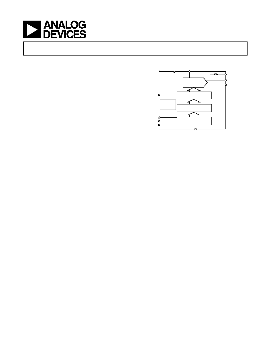
FUNCTIONAL BLOCK DIAGRAM
GENERAL DESCRIPTION
The AD5425 is a CMOS 8-bit current output digital-to-analog
converter that operates from a 2.5 V to 5.5 V power supply,
making it suited to battery-powered applications and many
other applications.
This DAC utilizes a double buffered 3-wire serial interface that
is compatible with SPI
®
, QSPITM, MICROWIRETM, and most
DSP interface standards. In addition, an
LDAC pin is provided,
which allows simultaneous update in a multi-DAC configuration.
On power-up, the internal shift register and latches are filled
with 0s and the DAC outputs are at 0 V.
As a result of processing on a CMOS submicron process, this
DAC offers excellent 4-quadrant multiplication characteristics,
with large signal multiplying bandwidths of 10 MHz.
The applied external reference input voltage (V
REF
) determines
the full-scale output current. An integrated feedback resistor (R
FB
)
provides temperature tracking and full-scale voltage output
when combined with an external I-to-V precision amplifier.
The AD5425 DAC is available in a small 10-lead MSOP package.
SCLK
SYNC
AD5425
V
REF
I
OUT
2
I
OUT
1
R
FB
R
8-BIT
R-2R DAC
DAC REGISTER
SDIN
V
DD
GND
POWER-ON
RESET
LDAC
CONTROL LOGIC AND
INPUT SHIFT REGISTER
INPUT LATCH
*Protected by U.S. Patent No. 5,969,657; other patents pending.

REV. 0
2
AD5425SPECIFICATIONS
1
(V
DD
= 2.5 V to 5.5 V, V
REF
= 10 V, I
OUT
x = O V. All specifications T
MIN
to T
MAX
, unless
otherwise noted. DC performance measured with OP177, AC performance with
AD8038, unless otherwise noted.)
Parameter
Min
Typ
Max
Unit
Conditions
STATIC PERFORMANCE
Resolution
8
Bits
Relative Accuracy
0.25
LSB
Differential Nonlinearity
0.5
LSB
Guaranteed monotonic
Gain Error
±10
mV
Gain Error Temperature Coefficient
2
±5
ppm FSR/
°C
Output Leakage Current
±5
nA
Data = 0x0000, T
A
= 25
°C, I
OUT
±25
nA
Data = 0x0000, I
OUT
REFERENCE INPUT
2
Reference Input Range
±10
V
V
REF
Input Resistance
8
10
12
k
Input resistance TC = 50 ppm/
°C
R
FB
Resistance
8
10
12
k
Input resistance TC = 50 ppm/
°C
Input Capacitance
Code Zero Scale
3
6
pF
Code Full Scale
5
8
pF
DIGITAL INPUTS
Input High Voltage, V
IH
1.7
V
Input Low Voltage, V
IL
0.6
V
Input Leakage Current, I
IL
2
A
Input Capacitance
4
10
pF
DYNAMIC PERFORMANCE
2
Reference Multiplying Bandwidth
10
MHz
V
REF
=
±3.5 V; DAC loaded all 1s
Output Voltage Settling Time
50
100
ns
Measured to
±16 mV. R
LOAD
= 100
, C
LOAD
=
15 pF DAC latch alternately loaded with 0s and 1s
Digital Delay
40
75
ns
10% to 90% Settling Time
15
30
ns
Rise and Fall time, V
REF
= 10 V, R
LOAD
= 100
Digital-to-Analog Glitch Impulse
2
nV-s
1 LSB change around major carry V
REF
= 0 V
Multiplying Feedthrough Error
70
dB
DAC latch loaded with all 0s. V
REF
=
±3.5 V, 1 MHz
48
dB
10 MHz
Output Capacitance
I
OUT
2
22
25
pF
All 0s loaded
10
12
pF
All 1s loaded
I
OUT
1
12
17
pF
All 0s loaded
25
30
pF
All 1s loaded
Digital Feedthrough
0.1
nV-s
Feedthrough to DAC output with
SYNC high and
alternate loading of all 0s and all 1s
Total Harmonic Distortion
81
dB
V
REF
= 3.5 V pk-pk; all 1s loaded, f = 1 kHz
Digital THD Clock = 1 MHz
50 kHz f
OUT
70
dB
8k Codes
Output Noise Spectral Density
25
nV
Hz
@ 1 kHz
SFDR Performance (Wide Band)
8k Codes, V
REF
= 3.5 V
Clock = 2 MHz
50 kHz f
OUT
55
dB
20 kHz f
OUT
63
dB
SFDR Performance (Narrow Band)
Clock = 2 MHz
50 kHz f
OUT
73
dB
20 kHz f
OUT
80
dB
Intermodulation Distortion
8k codes, V
REF
= 3.5 V
Clock = 2 MHz
f
1
= 20 kHz, f
2
= 25 kHz
79
dB

REV. 0
AD5425
3
Parameter
Min
Typ
Max
Unit
Conditions
POWER REQUIREMENTS
Power Supply Range
2.5
5.5
V
I
DD
0.4
5
A
Logic inputs = 0 V or V
DD
0.6
A
T
A
= 25
°C, Logic inputs = 0 V or V
DD
NOTES
1
Temperature range is as follows: Y version: 40
°C to +125°C.
2
Guaranteed by design, not subject to production test.
Specifications subject to change without notice.

REV. 0
4
AD5425
TIMING CHARACTERISTICS
1, 2
Parameter
Limit at T
MIN
, T
MAX
Unit
Conditions/Comments
f
SCLK
50
MHz max
Max clock frequency
t
1
20
ns min
SCLK cycle time
t
2
8
ns min
SCLK high time
t
3
8
ns min
SCLK low time
t
4
13
ns min
SYNC falling edge to SCLK falling edge setup time
t
5
5
ns min
Data setup time
t
6
3
ns min
Data hold time
t
7
5
ns min
SYNC rising edge to SCLK falling edge
t
8
30
ns min
Minimum
SYNC high time
t
9
0
ns min
SCLK falling edge to
LDAC falling edge
t
10
12
ns min
LDAC pulse width
t
11
10
ns min
SCLK falling edge to
LDAC rising edge
NOTES
1
See Figure 1. Temperature range is as follows: Y version: 40
°C to +125°C.
Guaranteed by design and characterization, not subject to production test.
2
All input signals are specified with tr = tf = 1 ns (10% to 90% of V
DD
) and timed from a voltage level of (V
IL
+ V
IH
)/2.
Specifications subject to change without notice.
t
8
SCLK
SYNC
DIN
LDAC
2
LDAC
1
NOTES
1
ASYNCHRONOUS LDAC UPDATE MODE
2
SYNCHRONOUS LDAC UPDATE MODE
DB7
t
4
t
5
t
6
t
2
t
1
t
3
t
7
t
10
t
9
t
11
DB0
Figure 1. Timing Diagram
(V
DD
= 2.5 V to 5.5 V, V
REF
= 10 V, I
OUT
2 = O V. All specifications T
MIN
to T
MAX
, unless
otherwise noted.)
REV. 0
AD5425
5
CAUTION
ESD (electrostatic discharge) sensitive device. Electrostatic charges as high as 4000 V readily
accumulate on the human body and test equipment and can discharge without detection. Although the
AD5425 features proprietary ESD protection circuitry, permanent damage may occur on devices
subjected to high energy electrostatic discharges. Therefore, proper ESD precautions are recommended
to avoid performance degradation or loss of functionality.
ABSOLUTE MAXIMUM RATINGS
1
(T
A
= 25
°C, unless otherwise noted.)
V
DD
to GND . . . . . . . . . . . . . . . . . . . . . . . . . . . 0.3 V to +7 V
V
REF
, R
FB
to GND . . . . . . . . . . . . . . . . . . . . . . 12 V to +12 V
I
OUT
1, I
OUT
2 to GND . . . . . . . . . . . . . . . . . . . . 0.3 V to +7 V
Logic Inputs and Output
2
. . . . . . . . . . . 0.3 V to V
DD
+ 0.3 V
Operating Temperature Range
Extended Industrial (Y Version) . . . . . . . . 40
°C to +125°C
Storage Temperature Range . . . . . . . . . . . . . 65
°C to +150°C
Junction Temperature . . . . . . . . . . . . . . . . . . . . . . . . . . 150
°C
10-lead MSOP
JA
Thermal Impedance . . . . . . . . . . . 206
°C/W
Lead Temperature, Soldering (10 seconds) . . . . . . . . . . 300
°C
IR Reflow, Peak Temperature (<20 seconds) . . . . . . . . 235
°C
NOTES
1
Stresses above those listed under Absolute Maximum Ratings may cause perma-
nent damage to the device. This is a stress rating only and functional operation of
the device at these or any other conditions above those listed in the operational
sections of this specification is not implied. Exposure to absolute maximum rating
conditions for extended periods may affect device reliability. Only one absolute
maximum rating may be applied at any one time.
2
Overvoltages at SCLK,
SYNC, DIN, and LDAC will be clamped by internal diodes.
ORDERING GUIDE
Resolution
INL
Temperature
Package
Package
Model
(Bits)
(LSBs)
Range
Description
Branding
Option
AD5425YRM
8
±0.25
40
o
C to +125
o
C
MSOP
D1P
RM-10
AD5425YRM-REEL
8
±0.25
40
o
C to +125
o
C
MSOP
D1P
RM-10
AD5425YRM-REEL7
8
±0.25
40
o
C to +125
o
C
MSOP
D1P
RM-10
EVAL-AD5425EB
Evaluation Kit
REV. 0
6
AD5425
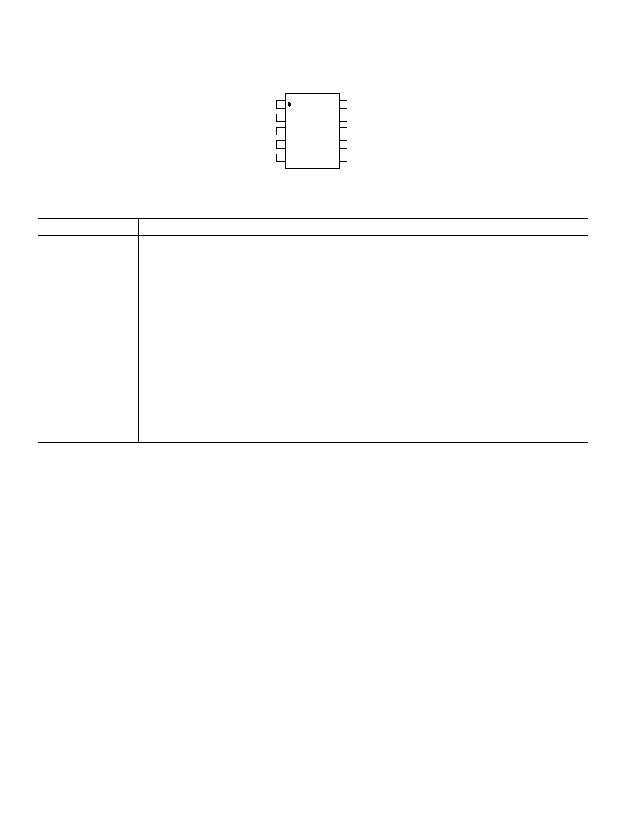
PIN CONFIGURATION
I
OUT
1
1
10
R
FB
SDIN
5
6
SYNC
SCLK
4
7
LDAC
GND
3
8
V
DD
I
OUT
2
2
9
V
REF
AD5425
(Not to Scale)
PIN FUNCTION DESCRIPTIONS
Pin No.
Mnemonic
Function
1
I
OUT
1
DAC Current Output.
2
I
OUT
2
DAC Analog Ground. This pin should normally be tied to the analog ground of the system.
3
GND
Digital Ground Pin.
4
SCLK
Serial Clock Input. Data is clocked into the input shift register on each falling edge of the serial clock input.
This device can accommodate clock rates of up to 50 MHz.
5
SDIN
Serial Data Input. Data is clocked into the 8-bit input register on each falling edge of the serial clock input.
6
SYNC
Active Low Control Input. This is the frame synchronization signal for the input data. When
SYNC goes
low, it powers on the SCLK and DIN buffers and the input shift register is enabled. Data is transferred on
each falling edge of the following 8 clocks.
7
LDAC
Load DAC Input. Updates the DAC output. The DAC is updated when this signal goes low or alternatively,
if this line is held permanently low, an automatic update mode is selected whereby the DAC is updated
after 8 SCLK falling edges with
SYNC low.
8
V
DD
Positive Power Supply Input. This part can be operated from a supply of 2.5 V to 5.5 V.
9
V
REF
DAC Reference Voltage Input Terminal.
10
R
FB
DAC Feedback Resistor Pin. Establishes voltage output for the DAC by connecting to external amplifier output.
REV. 0
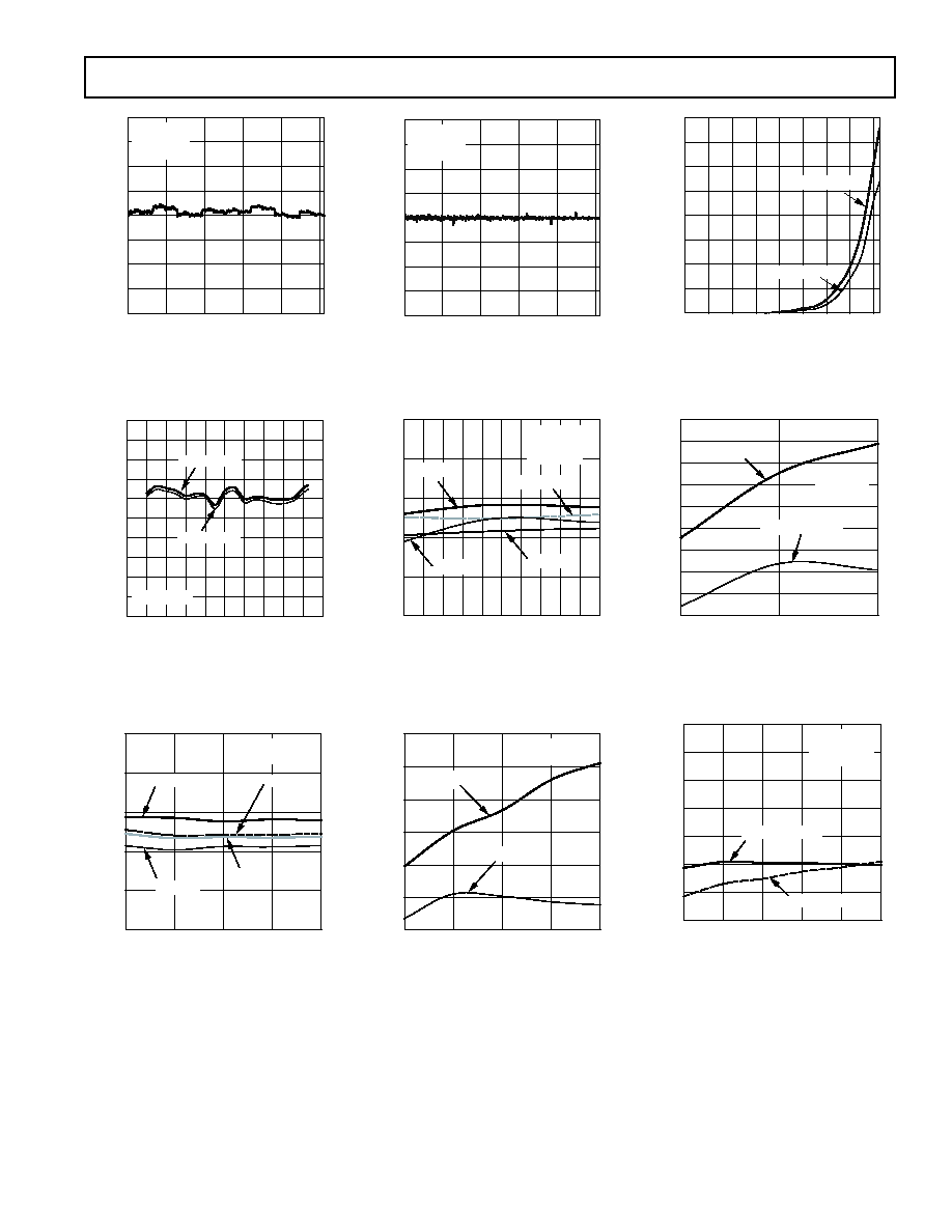
Typical Performance CharacteristicsAD5425
7
CODE
INL (LSB)
0.20
0.10
0.15
0
0.05
0.05
0.10
0.15
0.20
0
50
100
150
250
200
T
A
= 25 C
V
REF
= 10V
V
DD
= 5V
TPC 1. INL vs. Code (8-Bit DAC)
TEMPERATURE ( C)
ERROR (mV)
5
4
3
4
0
2
3
2
5
60 40 20
0
20
40
60
80 100 120 140
1
1
V
DD
= 5V
V
DD
= 2.5V
V
REF
= 10V
TPC 4. Gain Error vs. Temperature
0.5
0.3
0.1
0.1
0.3
0.5
LSBs
V
BIAS
(V)
1.0
0.5
1.5
2.0
2.5
MAX INL
MIN INL
MAX DNL
MIN DNL
V
DD
= 5V
V
REF
= 0V
TPC 7. Linearity vs. V
BIAS
Voltage Applied to I
OUT
2
0
0.2
0.4
0.6
0.8
1.0
1.2
1.4
40 20
0
20
40
60
80
100 120
TEMPERATURE ( C)
I
OUT
LEAKAGE (nA)
I
OUT
1 V
DD
5V
I
OUT
1 V
DD
3V
1.6
TPC 3. I
OUT
1
Leakage Current
vs. Temperature
0.4
0.2
0
0.2
0.4
0.6
0.8
1.0
1.2
1.4
VO
L
T
AG
E (mV)
V
BIAS
(V)
0.5
1.0
1.5
GAIN ERROR
OFFSET ERROR
T
A
= 25 C
V
DD
= 3V
V
REF
= 0V
TPC 6. Gain and Offset Errors vs.
V
BIAS
Voltage Applied to I
OUT
2
4.0
2.0
0
2.0
4.0
6.0
8.0
10.0
VOLTAGE (mV)
0
0.5
1.0
1.5
2.0
2.5
V
BIAS
(V)
GAIN ERROR
OFFSET ERROR
T
A
= 25 C
V
DD
= 5V
V
REF
= 2.5V
TPC 9. Gain and Offset Errors vs.
V
BIAS
Voltage Applied to I
OUT
2
CODE
DNL (LSB)
0.20
0.15
0.10
0.05
0.10
0.05
0
0.15
0.20
0
50
100
150
200
250
T
A
= 25 C
V
REF
= 10V
V
DD
= 5V
TPC 2. DNL vs. Code (8-Bit DAC)
0.5
0.3
0.1
0.1
0.3
0.5
LSBs
0.5 0.6 0.7 0.8 0.9 1.0 1.1 1.2 1.3 1.4 1.5
V
BIAS
(V)
MAX INL
MIN INL
MAX DNL
MIN DNL
T
A
= 25 C
V
DD
= 3V
V
REF
= 0V
TPC 5. Linearity vs. V
BIAS
Voltage Applied to I
OUT
2
0.5
0
0.5
1.0
1.5
2.0
2.5
VO
L
T
AG
E (mV)
V
BIAS
(V)
1.0
0.5
1.5
2.0
2.5
GAIN ERROR
OFFSET ERROR
V
DD
= 5V
V
REF
= 0V
TPC 8. Gain and Offset Errors
vs. Voltage Applied to I
OUT
2
REV. 0
8
AD5425
1.0
0.8
0.6
0.4
0.2
0
0.2
0.4
0.6
0.8
1.0
LSBs
V
BIAS
(V)
0.5
0
1.0
1.5
2.0
MAX INL BIAS
MIN INL BIAS
T
A
= 25 C
V
DD
= 5V
V
REF
= 2.5V
MAX DNL BIAS
MIN DNL BIAS
TPC 10. Linearity vs. V
BIAS
Voltage Applied to I
OUT
2
0.8
0.6
0.4
0.2
0
0.2
1
10
100
1k
10k 100k 1M
100M
FREQUENCY (Hz)
T
A
= 25 C
V
DD
= 5V
V
REF
= 3.5V
C
COMP
= 1.8pF
AD5445 AMPLIFIER
10M
GAIN (dB)
TPC 13. Reference Multiplying
Bandwidth--All 1s Loaded
9
6
3
0
3
10k
100k
1M
10M
100M
FREQUENCY (Hz)
T
A
= 25 C
VDD = 5V
AD8038 AMPLIFIER
V
REF
= 2V, AD8038 C
C
1.47pF
V
REF
= 2V, AD8038 C
C
1pF
V
REF
= 0.15V, AD8038 C
C
1pF
V
REF
= 0.15V, AD8038 C
C
1.47pF
V
REF
= 3.51V, AD8038 C
C
1.8pF
GAIN (dB)
TPC 16. Reference Multiply-
ing Bandwidth vs. Frequency
and Compensation Capacitor
VOLTAGE (V)
5.5
THRESHOLD VOLTAGE (V)
1.8
1.6
0
0.8
0.6
0.4
0.2
1.4
1.0
1.2
5.0
4.5
4.0
3.5
3.0
2.5
T
A
= 25 C
V
IL
V
IH
TPC 12. Threshold Voltages
vs. Supply Voltage
102
66
54
42
30
18
6
6
1
10
100
1k
10k 100k 1M 10M 100M
FREQUENCY (Hz)
GAIN (dB)
T
A
= 25 C
LOADING
ZS TO FS
0
60
48
36
24
12
84
72
78
90
96
T
A
= 25 C
V
DD
= 5V
V
REF
= 3.5V
INPUT
C
COMP
= 1.8pF
AD5445 AMPLIFIER
ALL ON
DB11
DB10
DB9
DB8
DB7
DB6
DB5
DB4
DB3
DB2
DB1
DB0
ALL OFF
TPC 15. Reference Multiply-
ing Bandwidth vs. Frequency
and Code
120
100
80
60
0
20
1
10
100
1k
10k
100k
1M
10M
FREQUENCY (Hz)
40
20
T
A
= 25 C
V
DD
= 3V
AMP = AD8038
FULL SCALE
ZERO SCALE
POWER SUPPLY REJECTION
TPC 18. Power Supply Rejec-
tion vs. Frequency
INPUT VOLTAGE (V)
CURRENT (mA)
0.7
0.6
0
0.5
0.4
0.3
5
4
3
2
1
0
0.2
0.1
V
DD
= 3V
V
DD
= 2.5V
V
DD
= 5V
T
A
= 25 C
TPC 11. Supply Current vs.
Input Voltage
TIME (ns)
OUTPUT VOLTAGE (V)
0.060
0.020
0.050
0.020
0.010
0.000
0.010
0.040
0.030
300
250
200
150
100
50
0
T
A
= 25 C
V
REF
= 0V
AD8038 AMP
C
COMP
= 1.8pF
AD5443
V
DD
3V, 0V REF
NRG = 0.088nVs
800H TO 7FFH
V
DD
5V, 0V REF
NRG = 0.119nVs,
800H TO 7FFH
V
DD
3V, 0V REF
NRG = 1.877nVs
7FFH TO 800H
V
DD
5V, 0V REF
NRG = 2.049nVs
7FFH TO 800H
TPC 14. Midscale Transition,
V
REF
= 3.5 V
90
85
80
65
60
1
10
100
1k
10k
100k
1M
FREQUENCY (Hz)
75
70
T
A
= 25 C
V
DD
= 3V
V
REF
= 3.5V p-p
THD + N (dB)
TPC 17. THD and Noise vs.
Frequency
REV. 0
AD5425
9
110
100
80
40
20
0
60
90
50
30
10
70
SFDR (dB)
0
200k
400k
600k
800k
1M
FREQUENCY (Hz)
T
A
= 25 C
V
DD
= 5V
V
REF
= 3.5V
AD8038 AMPLIFIER
C
COMP
= 1.8pF
8k CODES
TPC 19. Wideband SFDR,
Clock = 2 MHz, f
OUT
= 50 kHz
110
100
80
40
20
0
60
90
50
30
10
70
SFDR (dB)
25k 30k 35k 40k 45k 50k 55k 60k 65k 70k 75k
FREQUENCY (Hz)
T
A
= 25 C
V
DD
= 5V
V
REF
= 3.5V
AD8038 AMPLIFIER
C
COMP
= 1.8pF
8k CODES
TPC 22. Narrowband SFDR,
Clock = 2 MHz, f
OUT
= 50 kHz
110
100
80
40
20
0
60
90
50
30
10
70
SFDR (dB)
0
200k
400k
600k
800k
1M
FREQUENCY (Hz)
T
A
= 25 C
V
DD
= 5V
VREF = 3.5V
AD8038 AMPLIFIER
C
COMP
= 1.8pF
8k CODES
TPC 20. Wideband SFDR,
Clock = 2 MHz, f
OUT
= 20 kHz
100
90
80
70
60
50
40
30
20
10
0
IMD (dB)
10k
15k
20k
25k
30k
35k
FREQUENCY (Hz)
T
A
= 25 C
V
DD
= 5V
V
REF
= 3.5V
AD8038
AMPLIFIER
C
COMP
= 1.8pF
8k CODES
TPC 23. Narrowband IMD
( 50%) Clock = 2 MHz,
f
OUT
1 = 20 kHz, f
OUT
2 = 25 kHz
110
100
80
40
20
0
60
90
50
30
10
70
SFDR (dB)
10k 12k 14k 16k 18k 20k 22k 24k 26k 28k 30k
FREQUENCY (Hz)
T
A
= 25 C
V
DD
= 5V
V
REF
= 3.5V
AD8038 AMPLIFIER
C
COMP
= 1.8pF
8k CODES
TPC 21. Narrowband SFDR,
Clock = 2 MHz, f
OUT
= 20 kHz

REV. 0
10
AD5425
TERMINOLOGY
Relative Accuracy
Relative accuracy or endpoint nonlinearity is a measure of the
maximum deviation from a straight line passing through the end-
points of the DAC transfer function. It is measured after adjusting
for zero and full scale and is normally expressed in LSBs or as a
percentage of full-scale reading.
Differential Nonlinearity
Differential nonlinearity is the difference between the measured
change and the ideal 1 LSB change between any two adjacent
codes. A specified differential nonlinearity of 1 LSB max over
the operating temperature range ensures monotonicity.
Gain Error
Gain error or full-scale error is a measure of the output error
between an ideal DAC and the actual device output. For these
DACs, ideal maximum output is V
REF
1 LSB. Gain error of
the DACs is adjustable to 0 with external resistance.
Output Leakage Current
Output leakage current is current that flows in the DAC ladder
switches when these are turned off. For the I
OUT
1 terminal, it
can be measured by loading all 0s to the DAC and measuring
the I
OUT
1 current. Minimum current will flow in the I
OUT
2 line
when the DAC is loaded with all 1s.
Output Capacitance
Capacitance from I
OUT
1 or I
OUT
2 to AGND.
Output Current Settling Time
This is the amount of time it takes for the output to settle to a
specified level for a full-scale input change. For these devices, it
is specified with a 100
resistor to ground. The settling time
specification includes the digital delay from
SYNC rising edge
of the full scale output charge.
Digital-to-Analog Glitch lmpulse
The amount of charge injected from the digital inputs to the
analog output when the inputs change state. This is normally
specified as the area of the glitch in either pA-secs or nV-secs
depending upon whether the glitch is measured as a current or
voltage signal.
Digital Feedthrough
When the device is not selected, high frequency logic activity on
the device digital inputs is capacitively coupled through the
device to show up as noise on the I
OUT
pins and subsequently
into the following circuitry. This noise is digital feedthrough.
Multiplying Feedthrough Error
This is the error due to capacitive feedthrough from the DAC
reference input to the DAC I
OUT
1 terminal, when all 0s are
loaded to the DAC.
Total Harmonic Distortion (THD)
The DAC is driven by an ac reference. The ratio of the rms sum
of the harmonics of the DAC output to the fundamental value is
the THD. Usually only the lower order harmonices are included,
such as second to fifth.
Spurious-Free Dynamic Range (SFDR)
It is the usable dynamic range of a DAC before spurious noise
interferes or distorts the fundamental signal. SFDR is the
measure of difference in amplitude between the fundamental
and the largest harmonically or nonharmonically related spur
from dc to full Nyquist bandwidth (half the DAC sampling rate,
or fs/2). Narrow band SFDR is a measure of SFDR over an
arbitrary window size, in this case 50% of the fundamental.
Digital SFDR is a measure of the usable dynamic range of the
DAC when the signal is digitally generated sine wave.
THD
V
V
V
V
V
=
+
+
+
(
)
20
2
2
3
2
4
2
5
2
1
log
REV. 0
AD5425
11
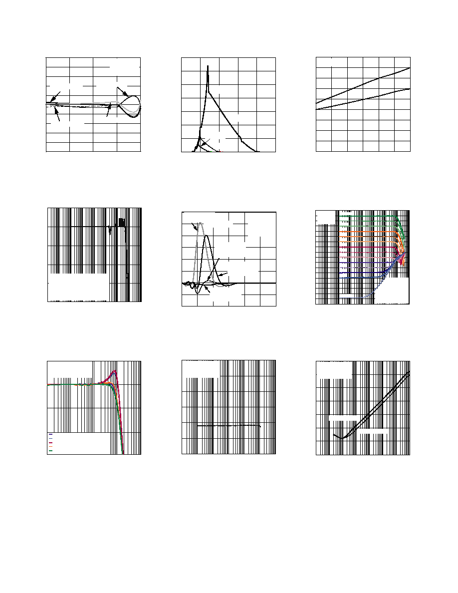
DAC SECTION
The AD5425 is an 8-bit current output DAC consisting of a
standard inverting R-2R ladder configuration. A simplified
diagram is shown in Figure 2. The feedback resistor R
FB
has a
value of R. The value of R is typically 10 k
(minimum 8 k
and maximum 12 k
). If I
OUT
1 and I
OUT
2 are kept at the same
potential, a constant current flows in each ladder leg, regardless
of digital input code. Therefore, the input resistance presented
at V
REF
is always constant and nominally of value R. The DAC
output (I
OUT
) is code-dependent, producing various resistances
and capacitances. External amplifier choice should take into
account the variation in impedance generated by the DAC on
the amplifiers inverting input node.
V
REF
I
OUT
2
DAC DATA LATCHES
AND DRIVERS
2R
S1
2R
S2
2R
S3
2R
S8
2R
R
R
R
I
OUT
1
R
FB
A
R
Figure 2. Simplified Ladder
Access is provided to the V
REF
, R
FB
, I
OUT
1 and I
OUT
2 terminals of
the DAC, making the device extremely versatile and allowing it to
be configured in several different operating modes, for example,
to provide a unipolar output, bipolar output, or in single-supply
modes of operation in unipolar mode or 4-quadrant multiplication
in bipolar mode. Note that a matching switch is used in series
with the internal R
FB
feedback resistor. If users attempt to mea-
sure R
FB
, power must be applied to V
DD
to achieve continuity.
SERIAL INTERFACE
The AD5425 has a simple 3-wire interface which is compatible
with SPI/QSPI/MICROWIRE and DSP interface standards. Data
is written to the device in 8 bit words. This 8-bit word consists
of 8 data bits as shown in Figure 3.
DB0 (LSB)
DB7 (MSB)
DATA BITS
DB7 DB6 DB5 DB4
DB3 DB2
DB0
DB1
Figure 3. 8-Bit Input Shift Register Contents
SYNC is an edge-triggered input that acts as a frame synchroni-
zation signal and chip enable. Data can be transferred into the
device only while
SYNC is low. To start the serial data transfer,
SYNC should be taken low, observing the minimum SYNC
falling to SCLK falling edge setup time, t
4
.
After loading eight data bits to the shift register, the
SYNC line is
brought high. The contents of the DAC register and the output
will be updated by bringing
LDAC low any time after the 8-bit
data transfer is complete as seen in the timing diagram of Figure 1.
LDAC may be tied permanently low if required. For another
serial transfer to take place, the interface must be enabled by
another falling edge of
SYNC.
Low Power Serial Interface
To minimize the power consumption of the device, the interface
powers up fully only when the device is being written to, i.e., on
the falling edge of
SYNC. The SCLK and SDIN input buffers
are powered down on the rising edge of
SYNC.
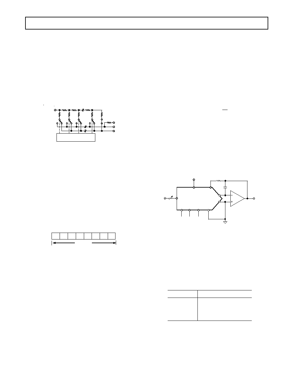
CIRCUIT OPERATION
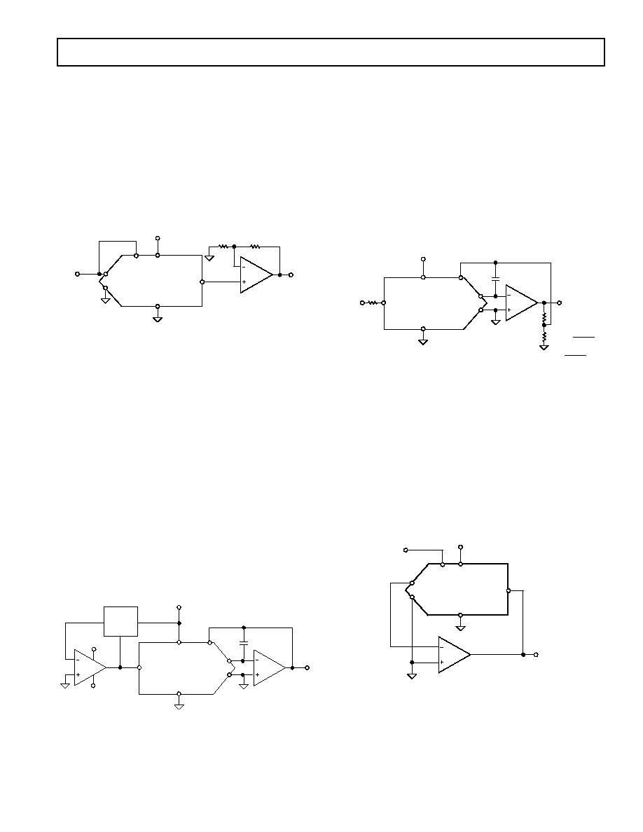
Unipolar Mode
Using a single op amp, this device can easily be configured to
provide 2-quadrant multiplying operation or a unipolar output
voltage swing as shown in Figure 4.
When an output amplifier is connected in unipolar mode, the
output voltage is given by:
V
V
OUT
REF
=
×
D
n
2
where D is the fractional representation of the digital word loaded
to the DAC, in this case 0 to 255, and n is the number of bits.
Note that the output voltage polarity is opposite to the V
REF
polarity for dc reference voltages.
This DAC is designed to operate with either negative or positive
reference voltages. The V
DD
power pin is used by only the internal
digital logic to drive the DAC switches' on and off states.
This DAC is also designed to accommodate ac reference input
signals in the range of 10 V to +10 V.
V
OUT
=
0 TO V
REF
SCLK SDIN
GND
V
REF
SYNC
I
OUT
2
I
OUT
1
R
FB
MICROCONTROLLER
AGND
AD5425
NOTES
1. R1 AND R2 USED ONLY IF GAIN ADJUSTMENT IS REQUIRED.
2. C1 PHASE COMPENSATION (1pF 2pF) MAY BE REQUIRED
IF A1 IS A HIGH SPEED AMPLIFIER.
R1
R2
A1
V
REF
V
DD
V
DD
C1
Figure 4. Unipolar Operation
With a fixed 10 V reference, the circuit shown in Figure 4 will
give an unipolar 0 V to 10 V output voltage swing. When V
IN
is an ac signal, the circuit performs 2-quadrant multiplication.
Table I shows the relationship between digital code and the
expected output voltage for unipolar operation.
Table I. Unipolar Code Table
Digital Input
Analog Output (V)
1111 1111
V
REF
(255/256)
1000 0000
V
REF
(128/256) = V
REF
/2
0000 0001
V
REF
(1/256)
0000 0000
V
REF
(0/256) = 0
REV. 0
12
AD5425
Bipolar Operation
In some applications, it may be necessary to generate full 4-quadrant
multiplying operation or a bipolar output swing. This can be
easily accomplished by using another external amplifier and some
external resistors as shown in Figure 5. In this circuit, the second
amplifier A2 provides a gain of 2. Biasing the external amplifier
with an offset from the reference voltage results in full 4-quadrant
multiplying operation. The transfer function of this circuit shows
that both negative and positive output voltages are created as the
input data (D) is incremented from code zero (V
OUT
= V
REF
)
to midscale (V
OUT
= 0 V ) to full scale (V
OUT
= + V
REF
).
V
V
V
OUT
REF
REF
=
×
(
)
-
D
n
/
2
1
Where D is the fractional representation of the digital word loaded
to the DAC and n is the resolution of the DAC.
When V
IN
is an ac signal, the circuit performs 4-quadrant
multiplication.
Table II shows the relationship between digital code and the
expected output voltage for bipolar operation.
Table II. Bipolar Code Table
Digital Input
Analog Output (V)
1111 1111
+V
REF
(127/128)
1000 0000
0
0000 0001
V
REF
(127/128)
0000 0000
V
REF
(128/128)
Stability
In the I-to-V configuration, the I
OUT
of the DAC and the inverting
node of the op amp must be connected as close as possible, and
proper PCB layout techniques must be employed. Since every
code change corresponds to a step function, gain peaking may
occur if the op amp has limited GBP and there is excessive para-
sitic capacitance at the inverting node. This parasitic capacitance
introduces a pole into the open-loop response, which can cause
ringing or instability in closed-loop applications.
An optional compensation capacitor, C1 can be added in parallel
with R
FB
for stability as shown in Figures 6 and 7. Too small a
value of C1 can produce ringing at the output, while too large a
value can adversely affect the settling time. C1 should be found
empirically but 1 pF2 pF is generally adequate for compensation.
SINGLE-SUPPLY APPLICATIONS
Current Mode Operation
Figure 6 shows a typical circuit for operation with a single 2.5 V
to 5 V supply. In the current mode circuit of Figure 6, I
OUT
2
and hence I
OUT
1 is biased positive by an amount applied to
V
BIAS
. In this configuration, the output voltage is given by
V
D
R
/ R
V
V
V
OUT
FB
DAC
BIAS
IN
BIAS
=
×
(
)
×
(
)
{
}
+
As D varies from 0 to 255, the output voltage varies from
V
V
toV
V
V
OUT
BIAS
OUT
BIAS
IN
=
= 2
V
OUT
V
DD
GND
V
IN
I
OUT
2
I
OUT
1
R
FB
V
DD
V
REF
V
BIAS
C1
NOTES
1. ADDITIONAL PINS OMITTED FOR CLARITY
2. C1 PHASE COMPENSATION (1pF2pF) MAY BE REQUIRED
IF A1 IS A HIGH SPEED AMPLIFIER.
A1
Figure 6. Single-Supply Current Mode Operation
V
BIAS
should be a low impedance source capable of sinking and
sourcing all possible variations in current at the I
OUT
2 terminal
without any problems.
It is important to note that V
IN
is limited to low voltages because
the switches in the DAC ladder no longer have the same source-
drain drive voltage. As a result their on resistance differs and this
degrades the linearity of the DAC.
V
OUT
=
V
REF
to +V
REF
SCLK SDIN
GND
V
REF
10V
SYNC
I
OUT
2
I
OUT
1
V
DD
V
REF
NOTES
1. R1 AND R2 ARE USED ONLY IF GAIN ADJUSTMENT IS REQUIRED.
ADJUST R1 FOR V
OUT
= 0 V WITH CODE 10000000 LOADED TO DAC.
2. MATCHING AND TRACKING IS ESSENTIAL FOR RESISTOR PAIRS R3 AND R4.
3. C1 PHASE COMPENSATION (1pF2pF) MAY BE REQUIRED IF A1/A2 IS
A HIGH SPEED AMPLIFIER.
AGND
R3
10k
AD5425
MICROCONTROLLER
R5
20k
R4
10k
A2
R1
V
DD
R
FB
R2
C1
A1
Figure 5. Bipolar Operation (4-Quadrant Multiplication)
REV. 0
AD5425
13
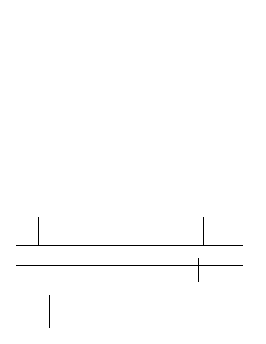
Voltage Switching Mode of Operation
Figure 7 shows this DAC operating in the voltage switching
mode. The reference voltage, V
IN
is applied to the I
OUT
1 pin,
I
OUT
2 is connected to AGND and the output voltage is available
at the V
REF
terminal. In this configuration, a positive reference
voltage results in a positive output voltage making single-supply
operation possible. The output from the DAC is voltage at a
constant impedance (the DAC ladder resistance), thus an op amp
is necessary to buffer the output voltage. The reference input no
longer sees a constant input impedance, but one that varies with
code. So, the voltage input should be driven from a low imped-
ance source.
V
OUT
V
DD
GND
V
IN
I
OUT
2
I
OUT
1
R
FB
V
DD
V
REF
NOTES
1. ADDITIONAL PINS OMITTED FOR CLARITY
2. C1 PHASE COMPENSATION (1pF 2pF) MAY BE REQUIRED
IF A1 IS A HIGH SPEED AMPLIFIER.
R2
R1
A1
Figure 7. Single-Supply Voltage Switching Mode Operation
It is important to note that V
IN
is limited to low voltage because
the switches in the DAC ladder no longer have the same source-
drain drive voltage. As a result, their on resistance differs, which
degrades the linearity of the DAC.
Also, V
IN
must not go negative by more than 0.3 V or an inter-
nal diode will turn on, exceeding the max ratings of the device.
In this type of application, the full range of multiplying capabil-
ity of the DAC is lost.
POSITIVE OUTPUT VOLTAGE
Note that the output voltage polarity is opposite to the V
REF
polarity for dc reference voltages. To achieve a positive voltage
output, an applied negative reference to the input of the DAC is
preferred over the output inversion through an inverting amplifier
because of the resistor tolerance errors. To generate a negative
reference, the reference can be level shifted by an op amp such
that the V
OUT
and GND pins of the reference become the virtual
ground and 2.5 V respectively, as shown in Figure 8.
V
OUT
=
0 TO +2.5V
V
DD
= 5V
GND
I
OUT
2
I
OUT
1
R
FB
V
DD
V
REF
C1
NOTES
1. ADDITIONAL PINS OMITTED FOR CLARITY
2. C1 PHASE COMPENSATION (1pF 2pF) MAY BE
REQUIRED IF A1 IS A HIGH SPEED AMPLIFIER.
GND
V
IN
V
OUT
ADR03
+5V
5V
1/2 AD8552
1/2 AD8552
2.5V
A1
A2
Figure 8. Positive Voltage Output with Minimum
of Components
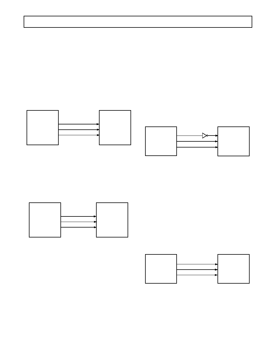
ADDING GAIN
In applications where the output voltage is required to be greater
than V
IN
, gain can be added with an additional external amplifier
or it can also be achieved in a single stage. It is important to
take into consideration the effect of temperature coefficients of
the thin film resistors of the DAC. Simply placing a resistor in
series with the R
FB
resistor will causing mismatches in the
temperature coefficients resulting in larger gain temperature
coefficient errors. Instead, the circuit of Figure 9 is a recom-
mended method of increasing the gain of the circuit. R1, R2,
and R3 should all have similar temperature coefficients, but
they need not match the temperature coefficients of the DAC.
This approach is recommended in circuits where gains of
greater than 1 are required.
V
OUT
V
DD
GND
I
OUT
2
I
OUT
1
R
FB
V
DD
V
REF
C1
NOTES
1. ADDITIONAL PINS OMITTED FOR CLARITY
2. C1 PHASE COMPENSATION (1pF 2pF) MAY BE
REQUIRED IF A1 IS A HIGH SPEED AMPLIFIER.
R
3
R
2
R2
V
IN
R1 = R2R3
R2 + R3
GAIN = R2 + R3
R2
A1
Figure 9. Increasing Gain of Current Output DAC
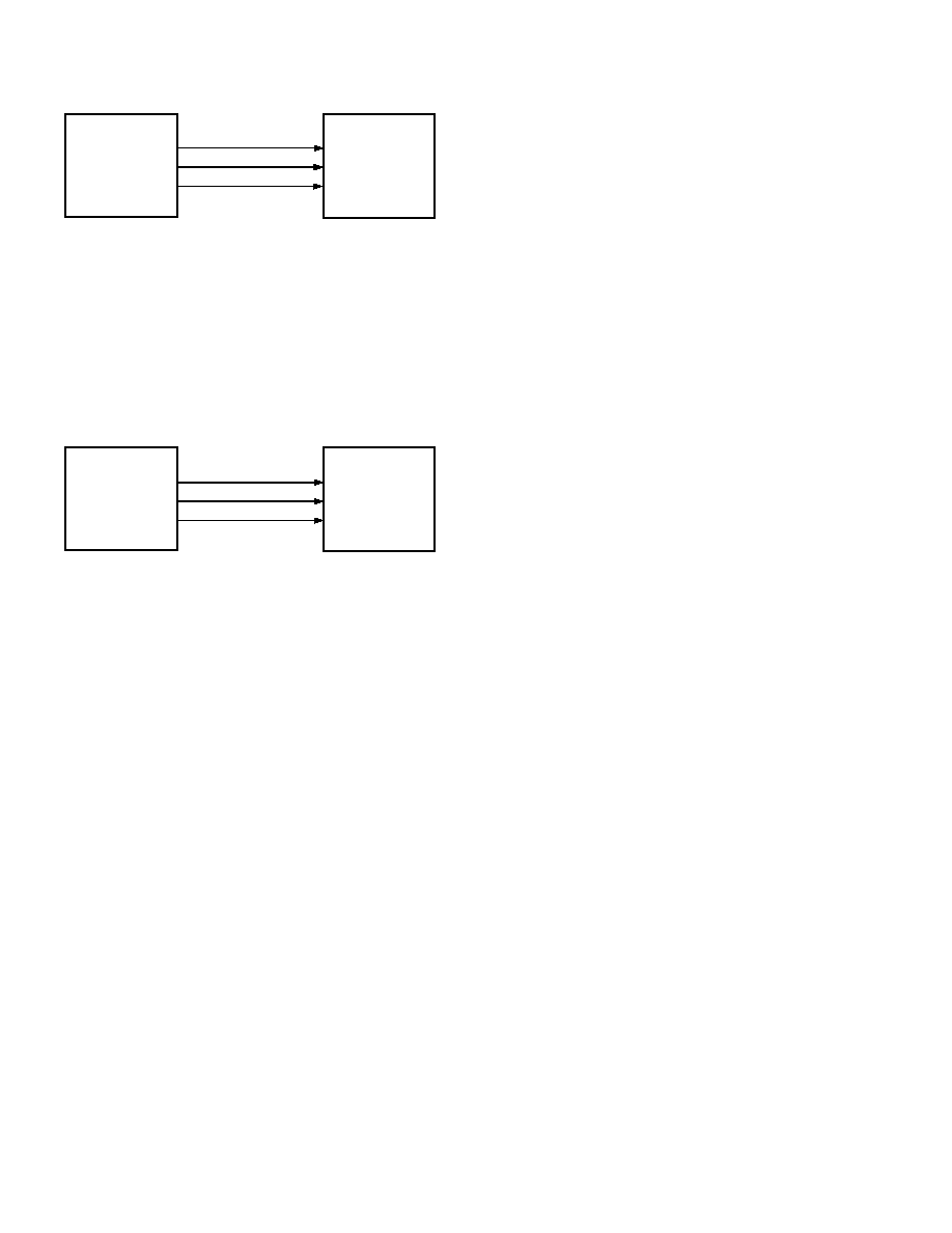
USED AS A DIVIDER OR PROGRAMMABLE GAIN
ELEMENT
Current steering DACs are very flexible and lend themselves to
many different applications. If this type of DAC is connected as the
feedback element of an op amp and R
FB
is used as the input resistor
as shown in Figure 10, then the output voltage is inversely pro-
portional to the digital input fraction D. For D = 1 2n the output
voltage is
V
V
/ D
V
/
OUT
IN
IN
n
=
=
(
)
1 2
V
OUT
V
DD
GND
V
IN
I
OUT
2
I
OUT
1
R
FB
V
DD
V
REF
NOTE
ADDITIONAL PINS OMITTED FOR CLARITY
A1
Figure 10. Current Steering DAC Used as a Divider
or Programmable Gain Element
As D is reduced, the output voltage increases. For small values
of the digital fraction D, it is important to ensure that the ampli-
fier does not saturate and also that the required accuracy is met.
For example, an eight bit DAC driven with the binary code 0
x/0
(00010000), i.e., 16 decimal, in the circuit of Figure 10 should
REV. 0
14
AD5425
cause the output voltage to be 16 V
IN
. However, if the DAC
has a linearity specification of 0.5 LSB, then D can in fact
have the weight anywhere in the range 15.5/256 to 16.5/256 so
that the possible output voltage will be in the range 15.5 V
IN
to
16.5 V
IN
--an error of +3% even though the DAC itself has a
maximum error of 0.2%.
DAC leakage current is also a potential error source in divider
circuits. The leakage current must be counterbalanced by an oppo-
site current supplied from the op amp through the DAC. Since
only a fraction D of the current into the V
REF
terminal is routed
to the I
OUT
1 terminal, the output voltage has to change as follows:
Output Error Voltage Due to DAC Leakage
Leakage
R / D
=
×
(
)
where R is the DAC resistance at the V
REF
terminal. For a DAC
leakage current of 10 nA, R = 10 k
and a gain (i.e., 1/D) of
16 the error voltage is 1.6 mV.
REFERENCE SELECTION
When selecting a reference for use with the AD5425 series of
current output DACs, pay attention to the reference's output
voltage temperature coefficient specification. This parameter not
only affects the full-scale error, but can also affect the linearity
(INL and DNL) performance. The reference temperature coeffi-
cient should be consistent with the system accuracy specifications.
For example, an 8-bit system required to hold its overall specifi-
cation to within 1 LSB over the temperature range 0
°C to 50°C
dictates that the maximum system drift with temperature should be
less than 78 ppm/
°C. A 12-bit system with the same temperature
range to overall specification within 2 LSB requires a maximum
drift of 10 ppm/
°C. By choosing a precision reference with low
output temperature coefficient, this error source can be mini-
mized. Table III suggests some of the suitable references available
from Analog Devices that are suitable for use with this range of
current output DACs.
AMPLIFIER SELECTION
The primary requirement for the current-steering mode is an
amplifier with low input bias currents and low input offset voltage.
The input offset voltage of an op amp is multiplied by the vari-
able gain (due to the code dependent output resistance of the DAC)
of the circuit. A change in this noise gain between two adjacent
digital fractions produces a step change in the output voltage
due to the amplifier's input offset voltage. This output voltage
change is superimposed on the desired change in output between
the two codes and gives rise to a differential linearity error, which
if large enough, could cause the DAC to be nonmonotonic. In
general, the input offset voltage should be a fraction (~<1/4) of
an LSB to ensure monotonic behavior when stepping through
codes.
The input bias current of an op amp also generates an offset at
the voltage output as a result of the bias current flowing in the
feedback resistor R
FB
. Most op amps have input bias currents
low enough to prevent any significant errors.
Common-mode rejection of the op amp is important in voltage
switching circuits, since it produces a code dependent error at
the voltage output of the circuit. Most op amps have adequate
common-mode rejection for use at 8-bit resolution.
Provided the DAC switches are driven from true wideband low
impedance sources (V
IN
and AGND), they settle quickly. Con-
sequently, the slew rate and settling time of a voltage switching
DAC circuit is determined largely by the output op amp. To obtain
minimum settling time in this configuration, it is important to
minimize capacitance at the V
REF
node (voltage output node in
this application) of the DAC. This is done by using low inputs
capacitance buffer amplifiers and careful board design.
Most single-supply circuits include ground as part of the analog
signal range, which in turns requires an amplifier that can
handle rail-to-rail signals. There is a large range of single-supply
amplifiers available from Analog Devices.
Table III. Suitable ADI Precision Voltage References Recommended for Use with AD5425 DACs
Part No.
Output Voltage
Initial Tolerance
Temperature Drift
0.1 Hz to 10 Hz Noise
Package
ADR01
10 V
0.1%
3 ppm/
°C
20 V p-p
SC70, TSOT, SOIC
ADR02
5 V
0.1%
3 ppm/
°C
10 V p-p
SC70, TSOT, SOIC
ADR03
2.5 V
0.2%
3 ppm/
°C
10 V p-p
SC70, TSOT, SOIC
ADR425
5 V
0.04%
3 ppm/
°C
3.4 V p-p
MSOP, SOIC
Table IV. Some Precision ADI Op Amps Suitable for Use with AD5425 DACs
Part No.
Max Supply Voltage (V)
V
OS
(max) ( V)
I
B
(max) (nA)
GBP (MHz)
Slew Rate (V/ s)
OP97
±20
25
0.1
0.9
0.2
OP1177
±18
60
2
1.3
0.7
AD8551
+6
5
0.05
1.5
0.4
Table V. Some High Speed ADI Op Amps Suitable for Use with AD5425 DACs
Max Supply Voltage
BW @ A
CL
Slew Rate
V
OS
(max)
I
B
(max)
Part No.
(V)
(MHz)
(V/ s)
( V)
(nA)
AD8065
±12
145
180
1500
0.01
AD8021
±12
200
100
1000
1000
AD8038
±5
350
425
3000
0.75
AD9631
±5
320
1300
10000
7000
REV. 0
AD5425
15
MICROPROCESSOR INTERFACING
Microprocessor interfacing to this DAC is via a serial bus that
uses standard protocol compatible with microcontrollers and DSP
processors. The communications channel is a 3-wire interface
consisting of a clock signal, a data signal, and a synchronization
signal. An
LDAC pin is also included. The AD5425 requires
an 8-bit word with the default being data valid on the falling
edge of SCLK, but this is changeable via the control bits in the
data-word.
ADSP-21xx to AD5425 Interface
The ADSP-21xx family of DSPs are easily interfaced to this family
of DACs without extra glue logic. Figure 11 shows an example
of an SPI interface between the DAC and the ADSP-2191.
SCK of the DSP drives the serial data line, DIN. SYNC is
driven from one of the port lines, in this case SPIxSEL.
SCLK
SCK
AD5425*
SYNC
SPIxSEL
SDIN
MOSI
ADSP-2191*
*ADDITIONAL PINS OMITTED FOR CLARITY
Figure 11. ADSP-2191 SPI to AD5425 Interface
A serial interface between the DAC and DSP SPORT is shown
in Figure 12. In this interface example, SPORT0 is used to
transfer data to the DAC shift register. Transmission is initiated
by writing a word to the Tx register after the SPORT has been
enabled. In a write sequence, data is clocked out on each rising
edge of the DSPs serial clock and clocked into the DAC input
shift register on the falling edge of its SCLK. The update of the
DAC output takes place on the rising edge of the
SYNC signal.
SCLK
SCLK
AD5425*
SYNC
TFS
SDIN
DT
ADSP-2101/
ADSP-2103/
ADSP-2191*
*ADDITIONAL PINS OMITTED FOR CLARITY
Figure 12. ADSP-2101/ADSP-2103/ADSP-2191 SPORT
to AD5425 Interface
Communication between two devices at a given clock speed is
possible when the following specifications are compatible: frame
sync delay and frame sync setup and hold, data delay and data
setup and hold, and SCLK width. The DAC interface expects a
t
4
(SYNC falling edge to SCLK falling edge setup time) of 13 ns
minimum. Consult the ADSP-21xx User Manual for information
on clock and frame sync frequencies for the SPORT register.
The SPORT Control Register should be set up as follows:
TFSW = 1, Alternate Framing
INVTFS = 1, Active Low Frame Signal
DTYPE = 00, Right Justify Data
ISCLK = 1, Internal Serial Clock
TFSR = 1, Frame Every Word
ITFS = 1, Internal Framing Signal
SLEN = 0111, 8-Bit Data-Word
80C51/80L51 to AD5425 Interface
A serial interface between the DAC and the 8051 is shown in
Figure 13. TxD of the 8051 drives SCLK of the DAC serial
interface, while RxD drives the serial data line, D
IN
. P3.3 is a
bit-programmable pin on the serial port and is used to drive
SYNC. When data is to be transmitted to the switch, P3.3 is
taken low. The 80C51/80L51 transmits data in 8-bit bytes
which is perfect for the AD5425 as it only requires an 8-bit
word. Data on RxD is clocked out of the microcontroller on
the rising edge of TxD and is valid on the falling edge. As
a result, no glue logic is required between the DAC and
microcontroller interface. P3.3 is taken high following the
completion of this cycle. The 8051 provides the LSB of its
SBUF register as the first bit in the data stream. The DAC
input register requires its data with the MSB as the first bit
received. The transmit routine should take this into account.
SCLK
TxD
8051*
SYNC
P1.1
SDIN
RxD
AD5425*
*ADDITIONAL PINS OMITTED FOR CLARITY
Figure 13. 80C51/80L51 to AD5425 Interface
MC68HC11 Interface to AD5425 Interface
Figure 14 shows an example of a serial interface between the DAC
and the MC68HC11 microcontroller. The serial peripheral
interface (SPI) on the MC68HC11 is configured for master mode
(MSTR = 1), clock polarity bit (CPOL) = 0, and the clock phase
bit (CPHA) = 1. The SPI is configured by writing to the SPI
control register (SPCR)--see the 68HC11 User Manual. SCK
of the 68HC11 drives the SCLK of the DAC interface, the
MOSI output drives the serial data line (D
IN
) of the AD5516. The
SYNC signal is derived from a port line (PC7). When data is being
transmitted to the AD5516, the
SYNC line is taken low (PC7).
Data appearing on the MOSI output is valid on the falling edge of
SCK. Serial data from the 68HC11 is transmitted in 8-bit bytes
with only eight falling clock edges occurring in the transmit cycle.
Data is transmitted MSB first. PC7 is taken high at the end of
the write.
SCLK
SCK
AD5425*
SYNC
PC7
SDIN
MOSI
MC68HC11*
*ADDITIONAL PINS OMITTED FOR CLARITY
Figure 14. 68HC11/68L11 to AD5425 Interface
MICROWIRE to AD5425 Interface
Figure 15 shows an interface between the DAC and any
MICROWIRE compatible device. Serial data is shifted out on
the falling edge of the serial clock, SK, and is clocked into the DAC
input shift register on the rising edge of SK, which corresponds
to the falling edge of the DAC's SCLK.
REV. 0
16
AD5425
SCLK
SK
MICROWIRE*
SYNC
CS
SDIN
SO
AD5425*
*ADDITIONAL PINS OMITTED FOR CLARITY
Figure 15. MICROWIRE to AD5425 Interface
PIC16C6x/7x to AD5425
The PIC16C6x/7x synchronous serial port (SSP) is configured
as an SPI master with the clock polarity bit (CKP) = 0. This is
done by writing to the synchronous serial port control register
(SSPCON). See the PIC16/17 Microcontroller User Manual.
In this example, I/O port RA1 is being used to provide a
SYNC signal and enable the serial port of the DAC. This
microcontroller transfers eight bits of data during each serial
transfer operation. Figure 16 shows the connection diagram.
SCLK
SCK/RC3
PIC16C6x/7x*
SYNC
RA1
SDIN
SDI/RC4
AD5425*
*ADDITIONAL PINS OMITTED FOR CLARITY
Figure 16. PIC16C6x/7x to AD5425 Interface
PCB LAYOUT AND POWER SUPPLY DECOUPLING
In any circuit where accuracy is important, careful consideration
of the power supply and ground return layout helps to ensure
the rated performance. The printed circuit board on which the
AD5425 is mounted should be designed so that the analog and
digital sections are separated and confined to certain areas of the
board. If the DAC is in a system where multiple devices require
an AGND-to-DGND connection, the connection should be
made at one point only. The star ground point should be estab-
lished as close as possible to the device.
These DACs should have ample supply bypassing of 10
µF in
parallel with 0.1
µF on the supply located as close to the pack-
age as possible, ideally right up against the device. The 0.1
µF
capacitor should have low effective series resistance (ESR) and
effective series inductance (ESI), such as the common ceramic
types that provide a low impedance path to ground at high
frequencies, to handle transient currents due to internal logic
switching. Low ESR 1
µF to 10 µF tantalum or electrolytic
capacitors should also be applied at the supplies to minimize
transient disturbance and to filter out low frequency ripple.
Fast switching signals such as clocks should be shielded with
digital ground to avoid radiating noise to other parts of the
board, and should never be run near the reference inputs.
Avoid crossover of digital and analog signals. Traces on opposite
sides of the board should run at right angles to each other. This
reduces the effects of feedthrough through the board. A micro-
strip technique is by far the best, but not always possible with a
double-sided board. In this technique, the component side of
the board is dedicated to ground plane while signal traces are
placed on the solder side.
It is good practice to employ compact, minimum lead length
PCB layout design. Leads to the input should be as short as
possible to minimize IR drops and stray inductance.
The PCB metal traces between V
REF
and R
FB
should also be
matched to minimize gain error. To maximize on high frequency
performance, the I-to-V amplifier should be located as close to
the device as possible.
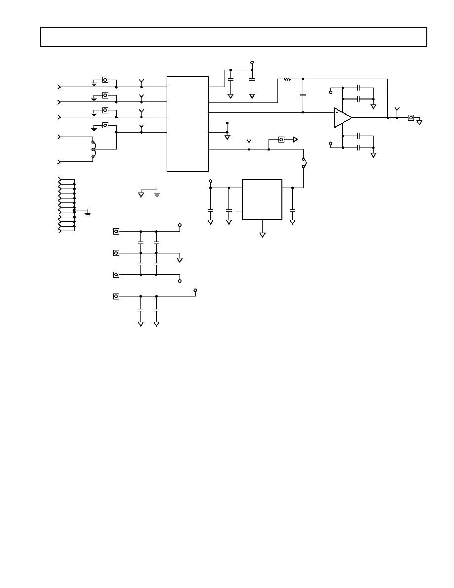
EVALUATION BOARD FOR THE AD5425 DAC
The board consists of an 8-bit AD5425 and a current to voltage
amplifier AD8065. Included on the evaluation board is a 10 V
reference ADR01. An external reference may also be applied via
an SMB input.
The evaluation kit consists of a CD-ROM with self-installing
PC software to control the DAC. The software simply allows the
user to write a code to the device.
OPERATING THE EVALUATION BOARD
Power Supplies
The board requires 12 V, and +5 V supplies. The +12 V V
DD
and V
SS
are used to power the output amplifier, while the +5 V
is used to power the DAC (V
DD1
) and transceivers (V
CC
).
Both supplies are decoupled to their respective ground plane
with 10
µF tantalum and 0.1 µF ceramic capacitors.
Link1 (LK1) is provided to allow selection between the on-board
reference (ADR01) or an external reference applied through J2.
Link2 should be connected to
LDAC position.
REV. 0
AD5425
17
V
DD
V
SS
V
OUT
P113
P15
P14
P12
P13
P119
P120
P121
P122
P123
P124
P125
P126
P127
P128
P129
P130
SCLK
SDIN
SYNC
LDAC
SCLK
SDIN
SYNC
SDO/
LDAC
SCLK
SDIN
SYNC
SDO/
LDAC
SDO
GND
I
OUT
2
V
DD
R
FB
V
REF
V
REF
V
DD1
V
REF
V
DD
+V
IN
V
OUT
TRIM
GND
I
OUT
1
AD5425/AD5426/
AD5432/AD5443
U1
U3
C5
4.7pF
C1
0.1 F
C2
10 F
C7
10 F
C8
0.1 F
P23
P22
P21
P24
AGND
V
SS
V
DD1
V
DD
C11
0.1 F
C12
10 F
C3
10 F
C4
0.1 F
C5
0.1 F
C13
0.1 F
C14
10 F
C15
0.1 F
C16
10 F
+
+
+
U2
ADR01AR
4
5
2
6
J2
J1
7
4
3
2
6
V
V+
+
+
C9
10 F
C10 0.1 F
+
TP1
R1 = 0
AD8065AR
8
10
4
5
6
1
2
3
7
9
J3
J4
J5
J6
LK2
LK1
A
B
Figure 17. Schematic of the AD5425 Evaluation Board
REV. 0
18
AD5425
EVALAD5425EB
P1
P2
J2
J6
J5
J4
U1
U3
C11
U2
J3
VREF
VREF
J1
VOUT
LK1
SDO/LDAC
SDO/LDAC
C10
C13
C14
C9
C1
R1
C2
C3
C6
C4
C16
C15
SYNC
SYNC
SDIN
SDIN
SCLK
SCLK
L
DAC
LK2
SDO
VDD
VSS
VDD1
A
GND
TP1
C8
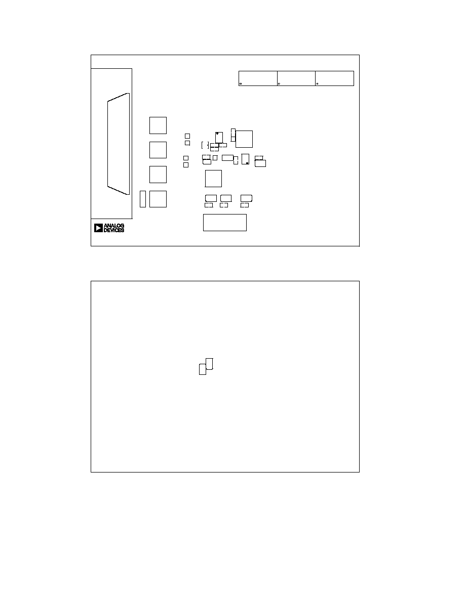
Figure 18. Silkscreen--Component Side View (Top Layer)
C7
C12
Figure 19. Silkscreen--Component Side View (Bottom Layer)

REV. 0
AD5425
19
Overview of AD54xx Devices
Part No.
Resolution
No. DACs
INL
t
S
max
Interface
Package
Features
AD5403
*
8
2
±0.25 60 ns
Parallel
CP-40
10 MHz Bandwidth,
10 ns
CS Pulse Width,
4-Quadrant Multiplying Resistors
AD5410
*
8
1
±0.25 100 ns
Serial
RU-16
10 MHz Bandwidth, 50 MHz Serial,
4-Quadrant Multiplying Resistors
AD5413
*
8
2
±0.25 100 ns
Serial
RU-24
10 MHz Bandwidth, 50 MHz Serial,
4-Quadrant Multiplying Resistors
AD5424
8
1
±0.25 60 ns
Parallel
RU-16, CP-20 10 MHz Bandwidth,
17 ns
CS Pulse Width
AD5425
8
1
±0.25 100 ns
Serial
RM-10
Byte Load, 10 MHz Bandwidth,
50 MHz Serial
AD5426
8
1
±0.25 100 ns
Serial
RM-10
10 MHz Bandwidth, 50 MHz Serial
AD5428
8
2
±0.25 60 ns
Parallel
RU-20
10 MHz Bandwidth,
17 ns
CS Pulse Width
AD5429
8
2
±0.25 100 ns
Serial
RU-10
10 MHz Bandwidth, 50 MHz Serial
AD5450
8
1
±0.25 100 ns
Serial
RJ-8
10 MHz Bandwidth, 50 MHz Serial
AD5404
*
10
2
±0.5
70 ns
Parallel
CP-40
10 MHz Bandwidth,
17 ns
CS Pulse Width,
4-Quadrant Multiplying Resistors
AD5411
*
10
1
±0.5
110 ns
Serial
RU-16
10 MHz Bandwidth, 50 MHz Serial,
4-Quadrant Multiplying Resistors
AD5414
*
10
2
±0.5
110 ns
Serial
RU-24
10 MHz Bandwidth, 50 MHz Serial,
4-Quadrant Multiplying Resistors
AD5432
10
1
±0.5
110 ns
Serial
RM-10
10 MHz Bandwidth, 50 MHz Serial
AD5433
10
1
±0.5
70 ns
Parallel
RU-20, CP-20 10 MHz Bandwidth,
17 ns
CS Pulse Width
AD5439
10
2
±0.5
110 ns
Serial
RU-16
10 MHz Bandwidth, 50 MHz Serial
AD5440
10
2
±0.5
70 ns
Parallel
RU-24
10 MHz Bandwidth,
17 ns
CS Pulse Width
AD5451
10
1
±0.25 110 ns
Serial
RJ-8
10 MHz Bandwidth, 50 MHz Serial
AD5405
12
2
±1
120 ns
Parallel
CP-40
10 MHz Bandwidth,
17 ns
CS Pulse Width,
4-Quadrant Multiplying Resistors
AD5412
*
12
1
±1
160 ns
Serial
RU-16
10 MHz Bandwidth, 50 MHz Serial,
4-Quadrant Multiplying Resistors
AD5415
12
2
±1
160 ns
Serial
RU-24
10 MHz Bandwidth, 50 MHz Serial,
4-Quadrant Multiplying Resistors
AD5443
12
1
±1
160 ns
Serial
RM-10
10 MHz Bandwidth, 50 MHz Serial
AD5444
12
1
±0.5
160 ns
Serial
RM-10
10 MHz Bandwidth, 50 MHz Serial
AD5445
12
1
±1
120 ns
Parallel
RU-20, CP-20 10 MHz Bandwidth,
17 ns
CS Pulse Width
AD5446
14
1
±2
180 ns
Serial
RM-10
10 MHz Bandwidth, 50 MHz Serial
AD5447
12
2
±1
120 ns
Parallel
RU-24
10 MHz Bandwidth,
17 ns
CS Pulse Width
AD5449
12
2
±1
160 ns
Serial
RU-16
10 MHz Bandwidth,
17 ns
CS Pulse Width
AD5452
12
1
±0.5
160 ns
Serial
RJ-8, RM-8
10 MHz Bandwidth, 50 MHz Serial
AD5453
14
1
±2
180 ns
Serial
RJ-8, RM-8
10 MHz Bandwidth, 50 MHz Serial
*Future parts, contact factory for availability
REV. 0
D0316101/04(0)
20
AD5425
Back Page_w/Content
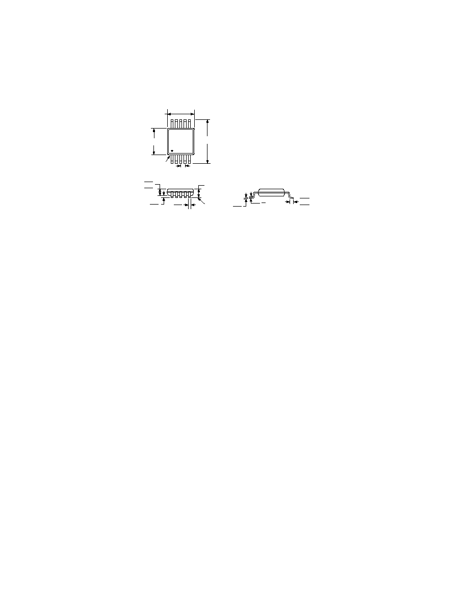
OUTLINE DIMENSIONS
10-Lead Mini Small Outline Package [MSOP]
(RM-10)
Dimensions shown in millimeters
0.23
0.08
0.80
0.60
0.40
8
0
0.15
0.00
0.27
0.17
0.95
0.85
0.75
SEATING
PLANE
1.10 MAX
10
6
5
1
0.50 BSC
3.00 BSC
3.00 BSC
4.90 BSC
PIN 1
COPLANARITY
0.10
COMPLIANT TO JEDEC STANDARDS MO-187BA
Document Outline
- FEATURES
- FUNCTIONAL BLOCK DIAGRAM
- GENERAL DESCRIPTION
- SPECIFICATIONS
- TIMING CHARACTERISTICS
- ABSOLUTE MAXIMUM RATINGS
- ORDERING GUIDE
- PIN CONFIGURATION
- PIN FUNCTION DESCRIPTIONS
- Typical Performance Characteristics
- TERMINOLOGY
- Relative Accuracy
- Differential Nonlinearity
- Gain Error
- Output Leakage Current
- Output Capacitance
- Output Current Settling Time
- Digital-to-Analog Glitch lmpulse
- Digital Feedthrough
- Multiplying Feedthrough Error
- Total Harmonic Distortion (THD)
- Spurious-Free Dynamic Range (SFDR)
- DAC SECTION
- SERIAL INTERFACE
- Low Power Serial Interface
- CIRCUIT OPERATION
- Unipolar Mode
- Bipolar Operation
- Stability
- SINGLE-SUPPLY APPLICATIONS
- Current Mode Operation
- Voltage Switching Mode of Operation
- POSITIVE OUTPUT VOLTAGE
- ADDING GAIN
- USED AS A DIVIDER OR PROGRAMMABLE GAIN ELEMENT
- REFERENCE SELECTION
- AMPLIFIER SELECTION
- MICROPROCESSOR INTERFACING
- ADSP-21xx to AD5425 Interface
- 80C51/80L51 to AD5425 Interface
- MC68HC11 Interface to AD5425 Interface
- MICROWIRE to AD5425 Interface
- PIC16C6x/7x to AD5425
- PCB LAYOUT AND POWER SUPPLY DECOUPLING
- EVALUATION BOARD FOR THE AD5425 DAC
- OPERATING THE EVALUATION BOARD
- Overview of AD54xx Devices
- OUTLINE DIMENSIONS