Äîêóìåíòàöèÿ è îïèñàíèÿ www.docs.chipfind.ru
REV. 0
Information furnished by Analog Devices is believed to be accurate and
reliable. However, no responsibility is assumed by Analog Devices for its
use, nor for any infringements of patents or other rights of third parties that
may result from its use. No license is granted by implication or otherwise
under any patent or patent rights of Analog Devices.
a
AD5516
*
One Technology Way, P.O. Box 9106, Norwood, MA 02062-9106, U.S.A.
Tel: 781/329-4700
www.analog.com
Fax: 781/326-8703
© Analog Devices, Inc., 2002
16-Channel, 12-Bit Voltage-Output DAC
with 14-Bit Increment Mode
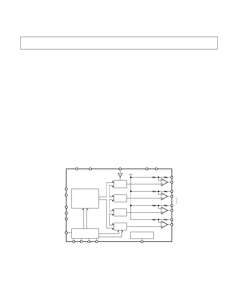
FUNCTIONAL BLOCK DIAGRAM
R
FB
0
RESET
BUSY
DACGND
AGND
DGND
DCEN
AD5516
DV
CC
AV
CC
V
DD
V
SS
V
OUT
0
R
FB
1
V
OUT
1
R
FB
14
V
OUT
14
R
FB
15
V
OUT
15
R
O F F S
R
F B
DAC
V
BIAS
R
O F F S
R
F B
DAC
R
O F F S
R
F B
DAC
R
O F F S
R
F B
DAC
REF_IN
PD
POWER-DOWN
LOGIC
SCLK
D
IN
D
OUT
SYNC
INTERFACE
CONTROL
LOGIC
7-BIT BUS
ANALOG
CALIBRATION
LOOP
12-BIT BUS
MODE1
MODE2
FEATURES
High Integration:
16-Channel DAC in 12 mm 12 mm
LFBGA
14-Bit Resolution via Increment/Decrement Mode
Guaranteed Monotonic
Low Power, SPI
TM
, QSPI
TM
,
MICROWIRE
TM
,
and DSP-
Compatible
3-Wire Serial Interface
Output Impedance 0.5
Output Voltage Range
2.5 V (AD5516-1)
5 V (AD5516-2)
10 V (AD5516-3)
Asynchronous Reset-Facility (via
RESET Pin)
Asynchronous Power-Down Facility (via PD Pin)
Daisy-Chain Mode
Temperature Range: 40 C to +85 C
APPLICATIONS
Level Setting
Instrumentation
Automatic Test Equipment
Optical Networks
Industrial Control Systems
Data Acquisition
Low Cost I/O
GENERAL DESCRIPTION
The AD5516 is a 16-channel, 12-bit voltage-output DAC. The
selected DAC register is written to via the 3-wire serial interface.
DAC selection is accomplished via address bits A3A0. 14-bit
resolution can be achieved by fine adjustment in Increment/
Decrement Mode (Mode 2). The serial interface operates at
clock rates up to 20 MHz and is compatible with standard SPI,
MICROWIRE, and DSP interface standards. The output volt-
age range is fixed at
±2.5 V (AD5516-1), ±5 V (AD5516-2),
and
±10 V (AD5516-3). Access to the feedback resistor in each
channel is provided via R
FB
0 to R
FB
15 pins.
The device is operated with AV
CC
= 5 V
± 5%, DV
CC
= 2.7 V to
5.25 V, V
SS
= 4.75 V to 12 V, and V
DD
= +4.75 V to +12 V
and requires a stable 3 V reference on REF_IN.
PRODUCT HIGHLIGHTS
1. Sixteen 12-bit DACs in one package, guaranteed monotonic
2. Available in a 74-lead LFBGA package with a body size of
12 mm 12 mm
*Protected by U.S. Patent No. 5,969,657; other patents pending
SPI and QSPI are trademarks of Motorola, Inc.
MICROWIRE is a trademark of National Semiconductor Corporation.

REV. 0
2
AD5516
Parameter
1
A Version
2
Unit
Conditions/Comments
DAC DC PERFORMANCE
Resolution
12
Bits
Integral Nonlinearity (INL)
±2
LSB max
Mode 1
Differential Nonlinearity (DNL)
1/+1.3
LSB max
±0.5 LSB typ, Monotonic; Mode 1
Increment/Decrement Step-Size
±0.25
LSB typ
Monotonic; Mode 2 Only
Bipolar Zero Error
±7
LSB max
Positive Full-Scale Error
±10
LSB max
Negative Full-Scale Error
±10
LSB max
VOLTAGE REFERENCE
REF_IN
Nominal Input Voltage
3
V
Input Voltage Range
3
2.875/3.125
V min/max
Input Current
±1
µA max
< 1 nA typ
ANALOG OUTPUTS (V
OUT
015)
Output Temperature Coefficient
3, 4
10
ppm/
°C typ
of FSR
DC Output Impedance
3
0.5
typ
Output Range
5
AD5516-1
±2.5
V typ
AD5516-2
±5
V typ
AD5516-3
±10
V typ
Resistive Load
3, 6
5
k
min
Capacitive Load
3, 6
200
pF
Short-Circuit Current
3
7
mA typ
DC Power-Supply Rejection Ratio
3
85
dB typ
V
DD
= +12 V
± 5%, V
SS
= 12 V
± 5%
DC Crosstalk
3
120
µV max
DIGITAL INPUTS
3
Input Current
±10
µA max
±5 µA typ
Input Low Voltage
0.8
V max
DV
CC
= 5 V
± 5%
0.4
V max
DV
CC
= 3 V
± 10%
Input High Voltage
2.4
V min
DV
CC
= 5 V
± 5%
2
V min
DV
CC
= 3 V
± 10%
Input Hysteresis (SCLK and
SYNC)
150
mV typ
Input Capacitance
10
pF max
5 pF typ
DIGITAL OUTPUTS (
BUSY, D
OUT
)
3
Output Low Voltage, DV
CC
= 5 V
0.4
V max
Sinking 200
µA
Output High Voltage, DV
CC
= 5 V
4
V min
Sourcing 200
µA
Output Low Voltage, DV
CC
= 3 V
0.4
V max
Sinking 200
µA
Output High Voltage, DV
CC
= 3 V
2.4
V min
Sourcing 200
µA
High Impedance Leakage Current (D
OUT
only)
±1
µA max
DCEN = 0
High Impedance Output Capacitance (D
OUT
only)
5
pF typ
DCEN = 0
POWER REQUIREMENTS
Power Supply Voltages
V
DD
+4.75/+15.75
V min/max
V
SS
4.75/15.75
V min/max
AV
CC
4.75/5.25
V min/max
DV
CC
2.7/5.25
V min/max
Power Supply Currents
7
I
DD
5
mA max
3.5 mA typ. All Channels Full-Scale
I
SS
5
mA max
3.5 mA typ. All Channels Full-Scale
AI
CC
17
mA max
13 mA typ
DI
CC
1.5
mA max
1 mA typ
Power-Down Currents
7
I
DD
2
µA max
200 nA typ
I
SS
3
µA max
200 nA typ
AI
CC
2
µA max
200 nA typ
DI
CC
2
µA max
200 nA typ
Power Dissipation
7
105
mW typ
V
DD
= +5 V, V
SS
= 5 V
NOTES
1
See Terminology section.
2
A Version: Industrial temperature range 40
°C to +85°C; typical at +25°C.
3
Guaranteed by design and characterization; not production tested.
4
AD780 as reference for the AD5516.
5
Output range is restricted from V
SS
+ 2 V to V
DD
2 V. Output span varies with reference voltage and is functional down to 2 V.
6
Ensure that you do not exceed T
J (MAX)
. See Absolute Maximum Ratings section.
7
Outputs unloaded.
Specifications subject to change without notice.
SPECIFICATIONS
(V
DD
= +4.75 V to +13.2 V, V
SS
= 4.75 V to 13.2 V; AV
CC
= 4.75 V to 5.25 V; DV
CC
=
2.7 V to 5.25 V; AGND = DGND = DACGND = 0 V; REF_IN = 3 V; All outputs unloaded.
All specifications T
MIN
to T
MAX
unless otherwise noted.)
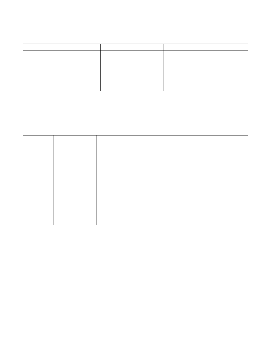
3
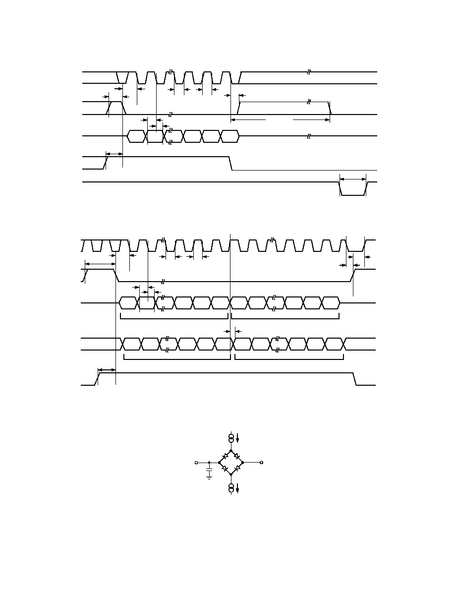
AC CHARACTERISTICS
AD5516
(V
DD
= +4.75 V to +13.2 V, V
SS
= 4.75 V to 13.2 V; AV
CC
= 4.75 V to 5.25 V; DV
CC
= 2.7 V to 5.25 V; AGND = DGND
= DACGND = 0 V; REF_IN = 3 V; All outputs unloaded. All specifications T
MIN
to T
MAX
unless otherwise noted.)
Parameter
1, 2
A Version
3
Unit
Conditions/Comments
Output Voltage Settling Time (Mode 1)
4
32
s max
100 pF, 5 k
Load Full-Scale Change
Output Voltage Settling Time (Mode 2)
4
2.5
s max
100 pF, 5 k
Load, 1 Code Increment
Slew Rate
0.85
V/ s typ
Digital-to-Analog Glitch Impulse
1
nV-s typ
1 LSB Change around Major Carry
Digital Crosstalk
5
nV-s typ
Analog Crosstalk AD5516-1
10
nV-s typ
Digital Feedthrough
1
nV-s typ
Output Noise Spectral Density @ 1 kHz
150
nV/(Hz)
1/2
typ
AD5516-1
NOTES
1
See Terminology section.
2
Guaranteed by design and characterization; not production tested.
3
A version: Industrial temperature range 40
°C to +85°C.
4
Timed from the end of a write sequence.
Specifications subject to change without notice.
Limit at T
MIN
, T
MAX
Parameter
1, 2, 3
(A Version)
Unit
Conditions/Comments
f
UPDATE1
32
kHz max
DAC Update Rate (Mode 1)
f
UPDATE2
750
kHz max
DAC Update Rate (Mode 2)
f
CLKIN
20
MHz max
SCLK Frequency
t
1
20
ns min
SCLK High Pulsewidth
t
2
20
ns min
SCLK Low Pulsewidth
t
3
15
ns min
SYNC Falling Edge to SCLK Falling Edge Setup Time
t
4
5
ns min
D
IN
Setup Time
t
5
5
ns min
D
IN
Hold Time
t
6
0
ns min
SCLK Falling Edge to
SYNC Rising Edge
t
7
10
ns min
Minimum
SYNC High Time (Standalone Mode)
t
7MODE2
400
ns min
Minimum
SYNC High Time (Daisy-Chain Mode)
t
8MODE1
10
ns min
BUSY Rising Edge to SYNC Falling Edge
t
9MODE2
200
ns min
18th SCLK Falling Edge to
SYNC Falling Edge (Standalone Mode)
t
10
10
ns min
SYNC Rising Edge to SCLK Rising Edge (Daisy-Chain Mode)
t
11
4
20
ns max
SCLK Rising Edge to D
OUT
Valid (Daisy-Chain Mode)
t
12
20
ns min
RESET Pulsewidth
NOTES
1
See Timing Diagrams in Figures 1 and 2.
2
Guaranteed by design and characterization; not production tested.
3
All input signals are specified with tr = tf = 5 ns (10% to 90% of DV
CC
) and timed from a voltage level of (V
IL
+ V
IH
)/2.
4
This is measured with the load circuit of Figure 3.
Specifications subject to change without notice.
TIMING CHARACTERISTICS
(V
DD
= +4.75 V to +13.2 V, V
SS
= 4.75 V to 13.2 V; AV
CC
= 4.75 V to 5.25 V; DV
CC
= 2.7 V to 5.25 V;
AGND = DGND = DACGND = 0 V. All specifications T
MIN
to T
MAX
unless otherwise noted.)
REV. 0
AD5516
4
SERIAL INTERFACE TIMING DIAGRAMS
t
12
SCLK
SYNC
DIN
BUSY
RESET
1
2
17
18
t
3
t
7
t
4
t
5
t
2
t
1
t
6
t
9
MODE2
t
8
MODE1
BIT 17
BIT 0
LSB
MSB
Figure 1. Serial Interface Timing Diagram
SCLK
SYNC
D
IN
D
OUT
BUSY
BIT 17
BIT 0
BIT 17
BIT 0
INPUT WORD FOR DEVICE N+1
UNDEFINED
INPUT WORD FOR DEVICE N
INPUT WORD FOR DEVICE N
BIT 17
BIT 0
t
7
MODE2
t
3
t
2
t
1
t
6
t
10
t
5
t
4
t
11
t
8
MODE1
LSB
MSB
Figure 2. Daisy-Chaining Timing Diagram
TO OUTPUT
PIN
C
L
50pF
200 A
I
OH
200 A
I
OL
1.6V
Figure 3. Load Circuit for D
OUT
Timing Specifications
REV. 0
AD5516
5
CAUTION
ESD (electrostatic discharge) sensitive device. Electrostatic charges as high as 4000 V readily
accumulate on the human body and test equipment and can discharge without detection. Although
the AD5516 features proprietary ESD protection circuitry, permanent damage may occur on
devices subjected to high-energy electrostatic discharges. Therefore, proper ESD precautions are
recommended to avoid performance degradation or loss of functionality.
WARNING!
ESD SENSITIVE DEVICE
ABSOLUTE MAXIMUM RATINGS
1, 2
(T
A
= 25
°C unless otherwise noted.)
V
DD
to AGND . . . . . . . . . . . . . . . . . . . . . . . . 0.3 V to +17 V
V
SS
to AGND . . . . . . . . . . . . . . . . . . . . . . . . +0.3 V to 17 V
AV
CC
to AGND, DACGND . . . . . . . . . . . . . . 0.3 V to +7 V
DV
CC
to DGND . . . . . . . . . . . . . . . . . . . . . . . 0.3 V to +7 V
Digital Inputs to DGND . . . . . . . . . . 0.3 V to DV
CC
+ 0.3 V
Digital Outputs to DGND . . . . . . . . . 0.3 V to DV
CC
+ 0.3 V
REF_IN to AGND, DACGND . . . . . 0.3 V to AV
CC
+ 0.3 V
V
OUT
015 to AGND . . . . . . . . . . . . V
SS
0.3 V to V
DD
+ 0.3 V
AGND to DGND . . . . . . . . . . . . . . . . . . . . 0.3 V to +0.3 V
R
FB
015 to AGND . . . . . . . . . . . . V
SS
0.3 V to V
DD
+ 0.3 V
Operating Temperature Range, Industrial . . . . . 40
°C to +85°C
Storage Temperature Range . . . . . . . . . . . . 65
°C to +150°C
Junction Temperature (T
J
MAX
) . . . . . . . . . . . . . . . . . . . 150
°C
74-Lead LFBGA Package,
JA
Thermal Impedance . . 41
°C/W
Reflow Soldering
Peak Temperature . . . . . . . . . . . . . . . . . . . . . . . . . . . 220
°C
Time at Peak Temperature . . . . . . . . . . . . . 10 sec to 40 sec
NOTES
1
Stresses above those listed under Absolute Maximum Ratings may cause permanent
damage to the device. This is a stress rating only; functional operation of the device
at these or any other conditions above those listed in the operational sections of this
specification is not implied. Exposure to absolute maximum rating conditions for
extended periods may affect device reliability.
2
Transient currents of up to 100 mA will not cause SCR latch-up.
ORDERING GUIDE
Model
Function
Output Voltage Span
Package Option
AD5516ABC-1
16 DACs
±2.5 V
74-Lead LFBGA
AD5516ABC-2
16 DACs
±5 V
74-Lead LFBGA
AD5516ABC-3
16 DACs
±10 V
74-Lead LFBGA
Document Outline
- Specifications
- Pinout
- Package Drawings
- Ordering Guide
- Features
- Applications
- Product Description
- Timing characteristics
- Absolute Maximum Ratings
- Functional Block Diagram
- Pin Function Description
- PRODUCT HIGHLIGHTS
- AC CHARACTERISTICS
- TIMING CHARACTERISTICS
- SERIAL INTERFACE TIMING DIAGRAMS
- CAUTION
- TERMINOLOGY
- FUNCTIONAL DESCRIPTION
- DIGITAL-TO-ANALOG SECTION
- SERIAL INTERFACE
- SYNC FUNCTION
- MICROPROCESSOR INTERFACING
- APPLICATION CIRCUITS
- POWER SUPPLY DECOUPLING
- DIAGRAMS
- Serial Interface Timing Diagram
- Daisy-Chaining Timing Diagram
- Load Circuit for DOUT Timing Specifications
- Mode 2 Data Format
- AD5516 to ADSP-2106x Interface
- AD5516 to PIC16C6x/7x Interface
- AD5516 to MC68HC11 Interface
- AD5516 to 8051 Interface
- AD5516 in an ATE System
- AD5516 in an Optical Control Loop