 | ÐлекÑÑоннÑй компоненÑ: AD5531 | СкаÑаÑÑ:  PDF PDF  ZIP ZIP |
Äîêóìåíòàöèÿ è îïèñàíèÿ www.docs.chipfind.ru
REV. 0
a
Information furnished by Analog Devices is believed to be accurate and
reliable. However, no responsibility is assumed by Analog Devices for its
use, nor for any infringements of patents or other rights of third parties that
may result from its use. No license is granted by implication or otherwise
under any patent or patent rights of Analog Devices.
One Technology Way, P.O. Box 9106, Norwood, MA 02062-9106, U.S.A.
Tel: 781/329-4700
www.analog.com
Fax: 781/326-8703
© Analog Devices, Inc., 2002
AD5530/AD5531
Serial Input, Voltage Output
12-/14-Bit DACs
SPI and QSPI are trademarks of Motorola, Inc.
MICROWIRE is a trademark of National Semiconductor Corporation.
FEATURES
Pin-Compatible 12- and 14-Bit DACs
Serial Input, Voltage Output
Maximum Output Voltage Range of 10 V
Data Readback
3-Wire Serial Interface
Clear Function to a User-Defined Voltage
Power-Down Function
Serial Data Output for Daisy-Chaining
16-Lead TSSOP Packages
APPLICATIONS
Industrial Automation
Automatic Test Equipment
Process Control
General-Purpose Instrumentation
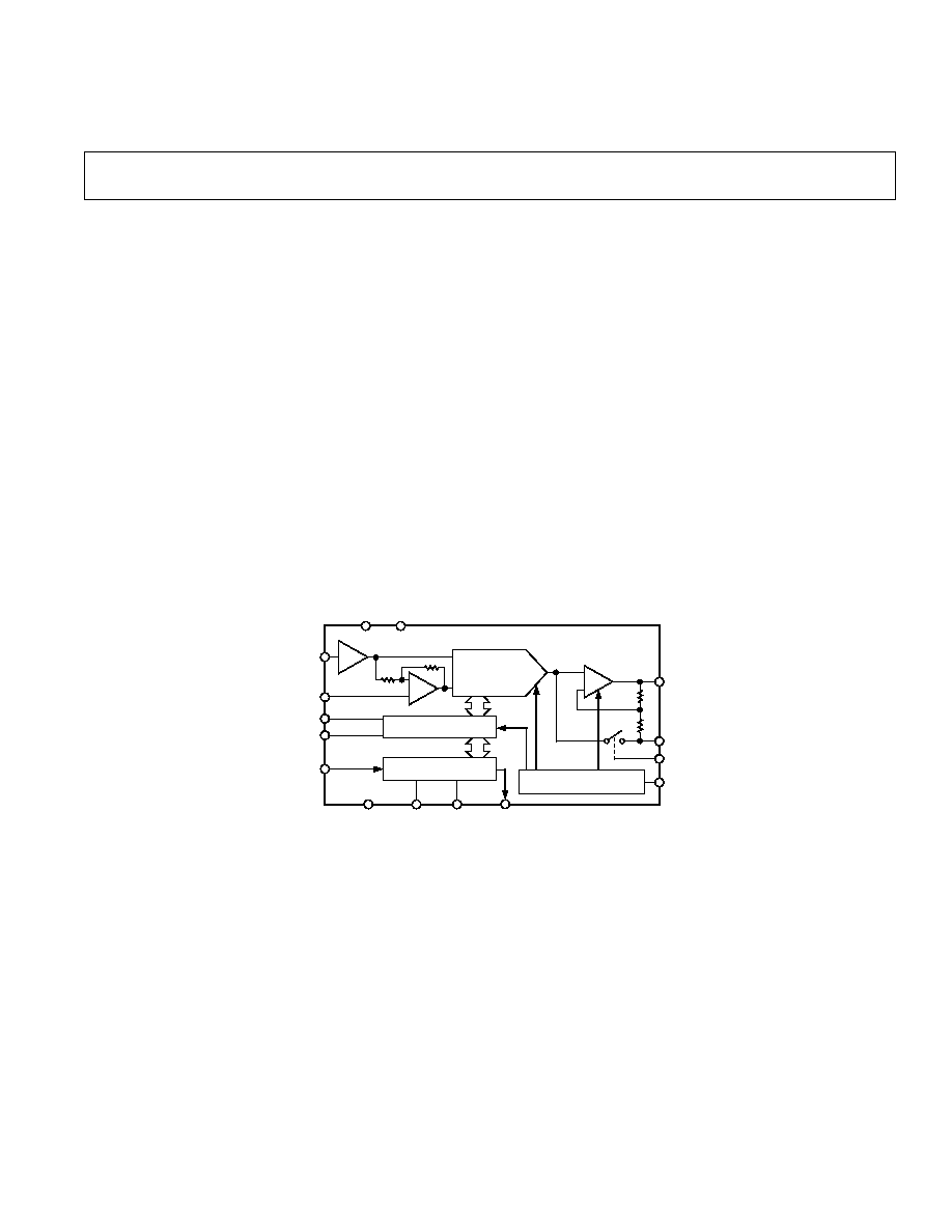
GENERAL DESCRIPTION
The AD5530 and AD5531 are single 12-/14-bit serial input,
voltage output DACs, respectively.
They utilize a versatile 3-wire interface that is compatible with
SPI
TM
, QSPI
TM
, MICROWIRE
TM
, and DSP interface standards.
Data is presented to the part in the format of a 16-bit serial word.
Serial data is available on the SDO pin for daisy-chaining pur-
poses. Data readback allows the user to read the contents of the
DAC register via the SDO pin.
The DAC output is buffered by a gain of 2 amplifier and refer-
enced to the potential at DUTGND.
LDAC may be used to update
the output of the DAC asynchronously. A power-down (
PD) pin
allows the DAC to be put into a low power state, and a
CLR pin
allows the output to be cleared to a user-defined voltage, the
potential at DUTGND.
The AD5530 and AD5531 are available in 16-lead TSSOP
packages.
FUNCTIONAL BLOCK DIAGRAM
SYNC
SCLK
GND
+
R
R
V
OUT
DUTGND
PD
SDO
V
SS
V
DD
RBEN
LDAC
+
R
R
REFIN
REFAGND
DAC REGISTER
SDIN
SHIFT REGISTER
12-/14-BIT DAC
POWER-DOWN
CONTROL LOGIC
CLR
AD5530/AD5531

REV. 0
2
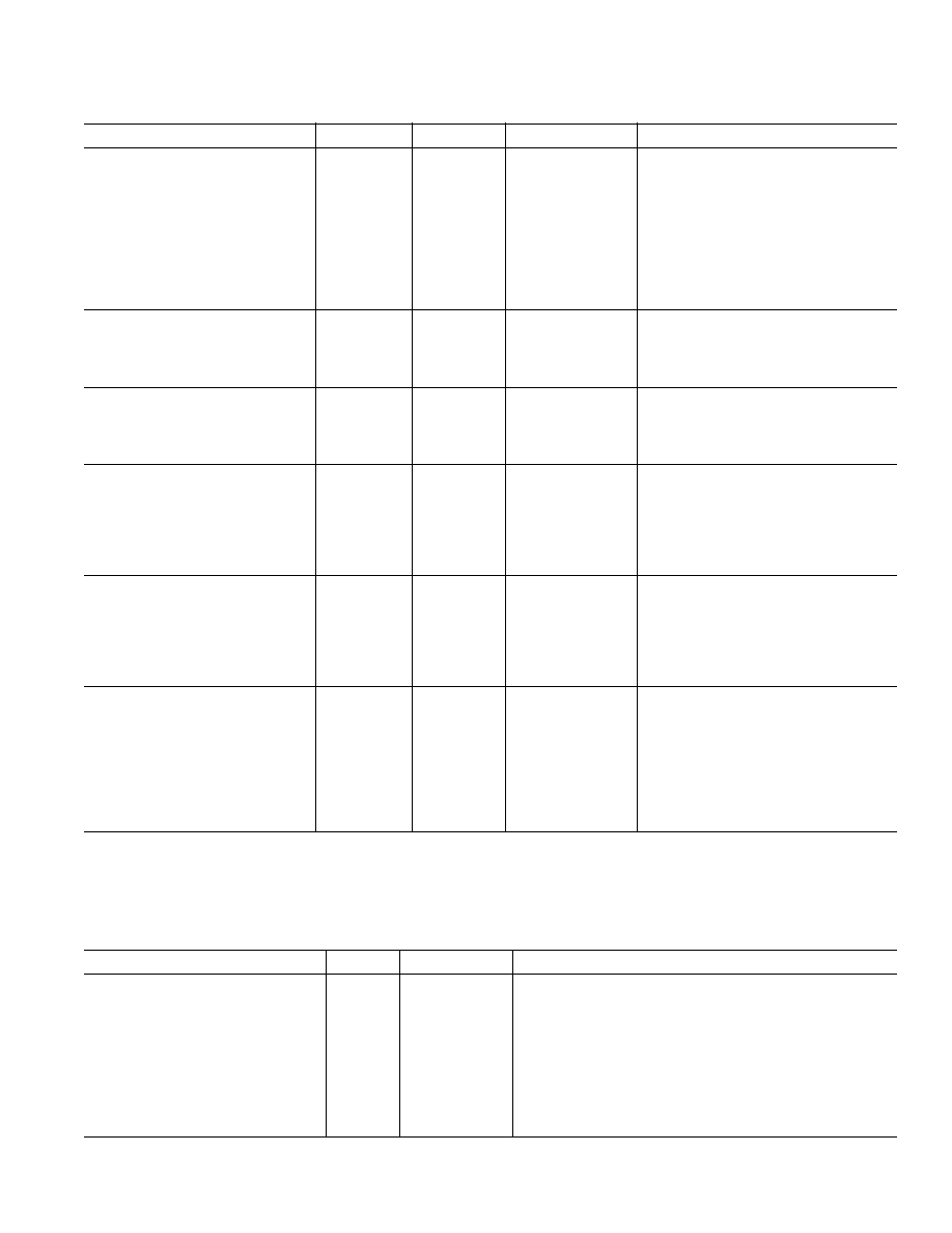
AD5530/AD5531SPECIFICATIONS
1
(V
DD
= +15 V
±
10%; V
SS
= 15 V
±
10%; GND = 0 V; R
L
= 5 k
and
C
L
= 220 pF to GND. All specifications T
MIN
to T
MAX
, unless otherwise noted.)
Parameter
AD5530
AD5531
Unit
Test Conditions/Comments
ACCURACY
Resolution
12
14
Bits
Relative Accuracy
±1
±2
LSB max
Differential Nonlinearity
±1
±1
LSB max
Guaranteed Monotonic Over Temperature
Zero-Scale Error
±2
±8
LSB max
Typically within
±1 LSB
Full-Scale Error
±2
±8
LSB max
Typically within
±1 LSB
Gain Error
±1
±4
LSB typ
Gain Temperature Coefficient
2
0.5
0.5
ppm FSR/
°C typ
10
10
ppm FSR/
°C max
REFERENCE INPUTS
2
Reference Input Range
0/5
0/5
V min/V max
Max Output Range
±10 V
DC Input Resistance
100
100
M
typ
Input Current
±1
±1
µA max
Per Input. Typically
±20 nA.
DUTGND INPUT
2
DC Input Impedance
60
60
k
typ
Max Input Current
±0.3
±0.3
mA typ
Input Range
4/+4
4/+4
V min/V max
Max Output Range
±10 V
O/P CHARACTERISTICS
2
Output Voltage Swing
±10
±10
V max
Short Circuit Current
15
15
mA max
Resistive Load
5
5
k
min
To 0 V
Capacitive Load
1200
1200
pF max
To 0 V
DC Output Impedance
0.5
0.5
max
DIGITAL I/O
V
INH
, Input High Voltage
2.4
2.4
V min
V
INL
, Input Low Voltage
0.8
0.8
V max
I
INH
, Input Current
±10
±10
µA max
Total for All Pins
C
IN
, Input Capacitance
2
10
10
pF max
3 pF Typ
SDO V
OL
Output Low Voltage
0.4
0.4
V max
I
SINK
= 1 mA
POWER REQUIREMENTS
V
DD
/V
SS
+15/15
+15/15
V nom
±10% For Specified Performance
Power Supply Sensitivity
Full Scale/V
DD
110
110
dB typ
Full Scale/V
SS
100
100
dB typ
I
DD
2
2
mA max
Outputs Unloaded
I
SS
2
2
mA max
Outputs Unloaded
I
DD
in Power-Down
150
150
µA max
Typically 50
µA
NOTES
1
Temperature range for B Version: 40
°C to +85°C.
2
Guaranteed by design, not subject to production test.
Specifications subject to change without notice.
REV. 0
AD5530/AD5531
3
Parameter
AD5530
AD5531
Unit
Test Conditions/Comments
ACCURACY
Resolution
12
14
Bits
Relative Accuracy
±1
±2
LSB max
Differential Nonlinearity
±1
±1
LSB max
Guaranteed Monotonic Over Temperature
Zero-Scale Error
±2
±8
LSB max
Typically within
±1 LSB
Full-Scale Error
±2
±8
LSB max
Typically within
±1 LSB
Gain Error
±1
±4
LSB typ
Gain Temperature Coefficient
2
0.5
0.5
ppm FSR/
°C typ
10
10
ppm FSR/
°C max
REFERENCE INPUTS
2
Reference Input Range
0/4.096
0/4.096
V min/V max
Max Output Range
±8.192 V
DC Input Resistance
100
100
M
typ
Input Current
±1
±1
µA max
Per Input. Typically
±20 nA.
DUTGND INPUT
2
DC Input Impedance
60
60
k
typ
Max Input Current
±0.3
±0.3
mA typ
Input Range
3/+3
3/+3
V min/V max
Max Output Range
±8.192 V
O/P CHARACTERISTICS
2
Output Voltage Swing
±8.192
±8.192
V max
Short Circuit Current
15
15
mA max
Resistive Load
5
5
k
min
To 0 V
Capacitive Load
1200
1200
pF max
To 0 V
DC Output Impedance
0.5
0.5
max
DIGITAL I/O
V
INH
, Input High Voltage
2.4
2.4
V min
V
INL
, Input Low Voltage
0.8
0.8
V max
I
INH
, Input Current
±10
±10
µA max
Total for All Pins
C
IN
, Input Capacitance
2
10
10
pF max
3 pF Typ
SDO V
OL
Output Low Voltage
0.4
0.4
V max
I
SINK
= 1 mA
POWER REQUIREMENTS
V
DD
/V
SS
+12/12
+12/12
V nom
±10% For Specified Performance
Power Supply Sensitivity
Full Scale/V
DD
110
110
dB typ
Full Scale/V
SS
100
100
dB typ
I
DD
2
2
mA max
Outputs Unloaded
I
SS
2
2
mA max
Outputs Unloaded
I
DD
in Power-Down
150
150
µA max
Typically 50
µA
NOTES
1
Temperature range for B Version: 40
°C to +85°C.
2
Guaranteed by design, not subject to production test.
Specifications subject to change without notice.
AC PERFORMANCE CHARACTERISTICS
Parameter
A
Unit
Test Conditions/Comments
DYNAMIC PERFORMANCE
Output Voltage Settling Time
20
µs typ
Full-Scale Change to
±1/2 LSB. DAC Latch Contents
alternately loaded with all 0s and all 1s.
Slew Rate
1.3
V/
µs typ
Digital-to-Analog Glitch Impulse
120
nV-s typ
DAC Latch alternately loaded with 0FFF Hex and
1000 Hex. Not dependent on load conditions.
Digital Feedthrough
0.5
nV-s typ
Effect of Input Bus Activity on DAC Output Under Test
Output Noise Spectral Density
@ 1 kHz
100
nV/(Hz)
1/2
typ
All 1s Loaded to DAC
Specifications subject to change without notice. Guaranteed by design, not subject to production test.
SPECIFICATIONS
1
(V
DD
= +12 V
±
10%; V
SS
= 12 V
±
10%; GND = 0 V;
R
L
= 5 k
and C
L
= 220 pF to GND; T
A
= T
MIN
to T
MAX
, unless otherwise noted.)
(V
DD
= 10.8 V to 16.5 V, V
SS
= 10.8 V to 16.5 V; GND = 0 V; R
L
= 5 k
and
C
L
= 220 pF to GND. All specifications T
MIN
to T
MAX
, unless otherwise noted.)
REV. 0
4
AD5530/AD5531
(V
DD
= 10.8 V to 16.5 V, V
SS
= 10.8 V to 16.5 V; GND = 0 V;
R
L
= 5 k
and C
L
= 220 pF to GND. All specifications T
MIN
to T
MAX
, unless otherwise noted.)
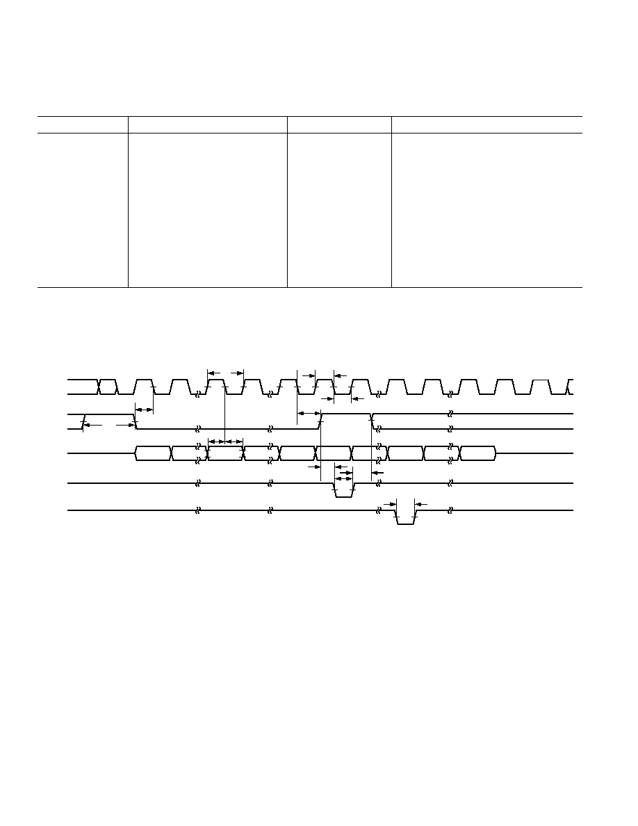
SCLK
SYNC
SDIN
LDAC*
CLR
*
LDAC MAY BE TIED PERMANENTLY LOW IF REQUIRED
t
1
DB15
DB14
DB11
DB0
MSB
LSB
t
4
t
6
t
7
t
8
t
12
t
9
t
10
t
11
t
5
t
3
t
2
Figure 1. Timing Diagram for Standalone Mode
STANDALONE TIMING CHARACTERISTICS
1, 2
Parameter
Limit at T
MIN
, T
MAX
Unit
Description
f
MAX
7
MHz max
SCLK Frequency
t
1
140
ns min
SCLK Cycle Time
t
2
60
ns min
SCLK Low Time
t
3
60
ns min
SCLK High Time
t
4
50
ns min
SYNC to SCLK Falling Edge Setup Time
t
5
40
ns min
SCLK Falling Edge to
SYNC Rising Edge
t
6
50
ns min
Min
SYNC High Time
t
7
40
ns min
Data Setup Time
t
8
15
ns min
Data Hold Time
t
9
5
ns min
SYNC High to LDAC Low
t
10
50
ns min
LDAC Pulsewidth
t
11
5
ns min
LDAC High to SYNC Low
t
12
50
ns min
CLR Pulsewidth
1
Guaranteed by design. Not production tested.
2
Sample tested during initial release and after any redesign or process change that may affect this parameter. All input signals are measured with tr = tf = 5 ns
(10% to 90% of V
DD
) and timed from a voltage level of (V
IL
+V
IH
)/2.
Specifications subject to change without notice.
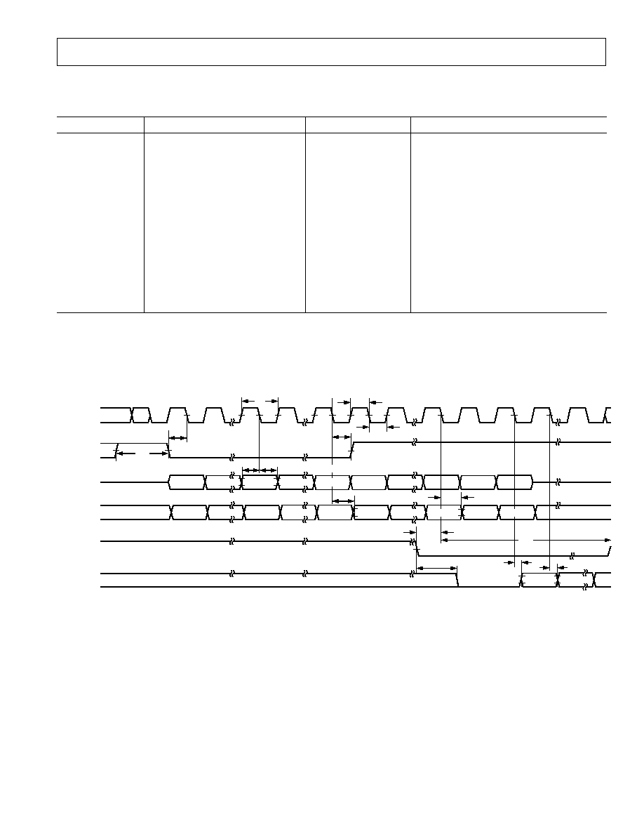
REV. 0
AD5530/AD5531
5
SCLK
SYNC
SDIN
t
1
DB15
DB14
DB11
MSB
t
4
t
6
t
7
t
8
t
5
t
3
t
2
SDO
(DAISY
CHAINING)
RBEN
SDO
(READBACK)
DB15
MSB
LSB
t
14
t
15
t
16
t
17
RB13
RB0
MSB
LSB
0
t
13
t
14
DB0
LSB
DB11
DB0
t
13
0
Figure 2. Timing Diagram for Daisy-Chaining and READBACK Mode
DAISY-CHAINING AND READBACK TIMING CHARACTERISTICS
1, 2, 3
Parameter
Limit at T
MIN
, T
MAX
Unit
Description
f
MAX
2
MHz max
SCLK Frequency
t
1
500
ns min
SCLK Cycle Time
t
2
200
ns min
SCLK Low Time
t
3
200
ns min
SCLK High Time
t
4
50
ns min
SYNC to SCLK Falling Edge Setup Time
t
5
40
ns min
SCLK Falling Edge to
SYNC Rising Edge
t
6
50
ns min
Min
SYNC High Time
t
7
40
ns min
Data Setup Time
t
8
15
ns min
Data Hold Time
t
12
50
ns min
CLR Pulsewidth
t
13
130
ns min
SCLK Falling Edge to SDO Valid
t
14
50
ns max
SCLK Falling Edge to SDO Invalid
t
15
50
ns min
RBEN to SCLK Falling Edge Setup Time
t
16
50
ns min
RBEN Hold Time
t
17
100
ns min
RBEN Falling Edge to SDO Valid
1
Guaranteed by design. Not production tested.
2
Sample tested during initial release and after any redesign or process change that may affect this parameter. All input signals are measured with tr = tf = 5 ns
(10% to 90% of V
DD
) and timed from a voltage level of (V
IL
+ V
IH
)/2.
3
SDO; R
PULLUP
= 5 k
, C
L
= 15 pF.
Specifications subject to change without notice.
(V
DD
= 10.8 V to 16.5 V, V
SS
= 10.8 V
to 16.5 V; V
SS
= 15 V
±10%; GND = 0 V; R
L
= 5 k
and C
L
= 220 pF to GND. All specifications T
MIN
to T
MAX
, unless otherwise noted.)