AD5535 32-Channel, 14-Bit DAC with Full-Scale Output Voltage Programmable from 50 V to 200 V Data Sheet (Rev. A)
32-Channel, 14-Bit DAC with Full-Scale Output
Voltage Programmable from 50 V to 200 V
AD5535
Rev. A
Information furnished by Analog Devices is believed to be accurate and reliable. However, no
responsibility is assumed by Analog Devices for its use, nor for any infringements of patents or other
rights of third parties that may result from its use. Specifications subject to change without notice.
No license is granted by implication or otherwise under any patent or patent rights of Analog
Devices. Trademarks and registered trademarks are the property of their respective owners.
One Technology Way, P.O. Box 9106, Norwood, MA 02062-9106, U.S.A.
Tel: 781.329.4700
www.analog.com
Fax: 781.461.3113
© 2005 Analog Devices, Inc. All rights reserved.
FEATURES
GENERAL DESCRIPTION
High integration
32-channel, 14-bit DAC with integrated high voltage
output amplifier
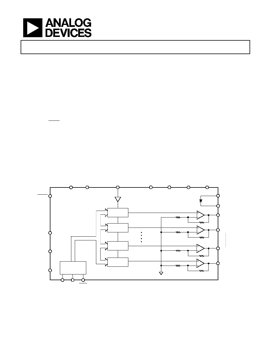
The AD5535 is a 32-channel, 14-bit DAC with an on-chip high
voltage output amplifier. This device is targeted for optical
micro-electromechanical systems. The output voltage range is
programmable via the REF_IN pin. The output range is 0 V to
50 V when REF_IN = 1 V, and 0 V to 200 V when REF_IN = 4 V.
Each amplifier can source 700 A, which is ideal for the
deflection and control of optical MEMS mirrors.
Guaranteed monotonic
Housed in 15 mm × 15 mm CSP_BGA package
Full-scale output voltage
Programmable from 50 V to 200 V via reference input
700 A drive capability
Integrated silicon diode for temperature monitoring
The selected DAC register is written to via the 3-wire interface.
The serial interface operates at clock rates of up to 30 MHz and
is compatible with DSP and microcontroller interface standards.
DSP-/microcontroller-compatible serial interface
1.2 MHz channel update rate
Asynchronous RESET facility
10°C to +85°C temperature range
APPLICATIONS
Optical micro-electromechanical systems (MEMS)
Optical crosspoint switches
Micropositioning applications using piezoelectric actuators
Level setting in automotive test and measurement
The device is operated with AV
CC
= 4.75 V to 5.25 V, DV
CC
=
2.7 V to 5.25 V, V
-
= -4.75 V to -5.25 V, V
+
= 4.75 V to 5.25 V,
and V
PP
= 210 V. REF_IN is buffered internally on the AD5535
and should be driven from a stable reference source.
FUNCTIONAL BLOCK DIAGRAM
RF
R1
RF
R1
RF
R1
RF
R1
INTERFACE
CONTROL
LOGIC
DAC
DAC
DAC
DAC
DV
CC
AV
CC
SYNC
D
IN
SCLK
DGND
AGND
DAC_GND
RESET
REF_IN
V
PP
PGND
V
V
+
14-BIT BUS
ANODE
CATHODE
V
OUT
0
V
OUT
1
V
OUT
30
V
OUT
31
AD5535
05068-001
Figure 1.

AD5535
Rev. A | Page 2 of 16
TABLE OF CONTENTS
Features .............................................................................................. 1
Applications....................................................................................... 1
General Description ......................................................................... 1
Functional Block Diagram .............................................................. 1
Specifications..................................................................................... 3
Timing Characteristics ................................................................ 5
Absolute Maximum Ratings............................................................ 6
ESD Caution.................................................................................. 6
Pin Configuration and Function Descriptions............................. 7
Typical Performance Characteristics ............................................. 9
Terminology .................................................................................... 11
Functional Description .................................................................. 12
DAC Section................................................................................ 12
Reset Function ............................................................................ 12
Serial Interface ............................................................................ 12
Microprocessor Interfacing....................................................... 12
Applications..................................................................................... 14
MEMS Mirror Control Application......................................... 14
IPC-221-Compliant Board Layout........................................... 14
Power Supply Sequencing and Decoupling
Recommendations...................................................................... 15
Guidelines for Printed Circuit Board Layout ......................... 15
Outline Dimensions ....................................................................... 16
Ordering Guide .......................................................................... 16
REVISION HISTORY
8/05--Rev. 0 to Rev. A
Changes to Table 3............................................................................ 6
Changes to Ordering Guide .......................................................... 16
5/05--Revision 0: Initial Version

AD5535
Rev. A | Page 3 of 16
SPECIFICATIONS
V
PP
= 210 V, V
-
= -5 V, V
+
= +5 V; AV
CC
= 5.25 V; DV
CC
= 2.7 V to 5.25 V; PGND = AGND = DGND = DAC_GND = 0 V;
REF_IN = 4.096 V; all outputs unloaded. All specifications T
MIN
to T
MAX
, unless otherwise noted.
Table 1.
A Grade
2
Parameter
1
Min
Typ
Max
Unit
Conditions/Comments
DC PERFORMANCE
3
Resolution
14
Bits
Integral Nonlinearity (INL)
±0.1
% of FSR
Differential Nonlinearity (DNL)
1
±0.5
+1
LSB
Guaranteed monotonic
Zero-Code Voltage
1
2.5
V
Output Offset Error
2
+2
V
Offset Drift
0.02
mV/°C
Voltage Gain
47.5
50
52.5
V/V
Gain Temperature Coefficient
5
ppm/°C
Channel-to-Channel Gain Match
4
5
+5
%
Full-Scale Voltage Drift
3
ppm/°C
OUTPUT CHARACTERISTICS
Output Voltage Range
3
2.5
V
PP
- 10
V
Output Impedance
50
Resistive Load
4, 5
1
M
Capacitive Load
4
200
pF
Short-Circuit Current
0.7
mA
DC Crosstalk
4
3
LSB
DC Power Supply Rejection (PSRR), V
PP
70
dB
AC CHARACTERISTICS
4
Settling Time
¼ to ¾ Scale Step
30
s
No load
65
s
200 pF load
1 LSB Step
10
s
No load
10
s
200 pF load
Slew Rate
10
V/s
No load
3
V/s
200 pF load
3 dB Bandwidth
5
kHz
Output Noise Spectral Density
4.5
V/Hz
Measured at 10 kHz
0.1 Hz to 10 Hz Output Noise Voltage
1
mV p-p
Digital-to-Analog Glitch Impulse
10
nV-s
1 LSB change around major carry
Analog Crosstalk
13
V-s
Digital Feedthrough
1
nV-s
VOLTAGE REFERENCE, REF_IN
6
AV
CC
must exceed REF_IN by 1.15 V min
Input Voltage Range
4
1
4.096
V
Input Current
1.25
A
TEMPERATURE MEASUREMENT DIODE
4
Peak Inverse Voltage, P
IV
5
V
Cathode to anode
Forward Diode Drop, V
F
0.65
0.8
V
I
F
= 100 A, anode to cathode
Forward Diode Current, I
F
100
A
Anode to cathode
V
F
Temperature Coefficient, T
C
-2.20
mV/°C
Anode to cathode

AD5535
Rev. A | Page 4 of 16
A Grade
2
Parameter
1
Min
Typ
Max
Unit
Conditions/Comments
DIGITAL INPUTS
4
Input Current
±5
±10
A
Input Low Voltage
0.8
V
Input High Voltage
2.0
V
Input Hysteresis (SCLK and SYNC Only)
200
mV
Input Capacitance
10
pF
POWER SUPPLY VOLTAGES
7
V
PP
(50 × REF_IN) + 10
225
V
V
5.25
4.75
V
V
+
4.75
5.25
V
AV
CC
4.75
5.25
V
DV
CC
2.7
5.25
V
POWER SUPPLY CURRENTS
7
I
PP
75
100
A/channel
I
-
2.3
3.5
mA
I
+
0.5
1
mA
AI
CC
15
18
mA
DI
CC
0.25
0.5
mA
POWER DISSIPATION
7
594
mW
1
See the Terminology section.
2
A Grade temperature range: -10°C to +85°C; typical = +25°C.
3
Linear output voltage range: +7 V to V
PP
- 10 V.
4
Guaranteed by design and characterization, not production tested.
5
Ensure that T
J
max is not exceeded. See the Absolute Maximum Ratings section.
6
Reference input determines output voltage range. Using a 4.096 V reference (REF198) gives an output voltage range of 2.50 V to 200 V. The output range is programmable
via the reference input. The full-scale output range is programmable from 50 V to 200 V. The linear output voltage range is restricted from 7 V to V
PP
- 10 V.
7
Outputs unloaded.
AD5535
Rev. A | Page 5 of 16
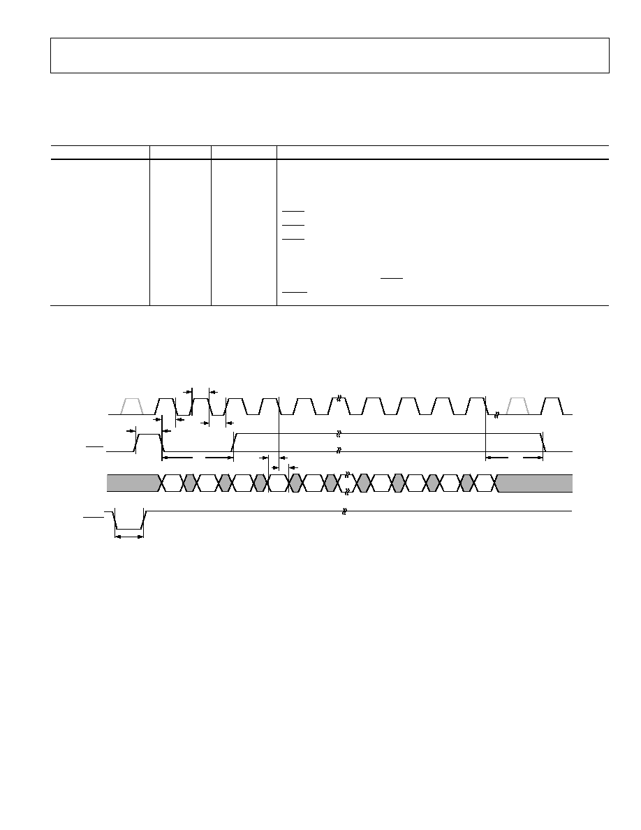
TIMING CHARACTERISTICS
V
PP
= 210 V, V
-
= 5 V, V
+
= +5 V; AV
CC
= 5.25 V; DV
CC
= 2.7 V to 5.25 V; AGND = DGND = DAC_GND = 0 V; REF_IN = 4.096 V.
All specifications T
MIN
to T
MAX
, unless otherwise noted.
Table 2.
Parameter
A Grade
Unit
Conditions/Comments
1 , ,
2 3
f
1.2
MHz max
Channel Update Rate
UPDATE
f
30
MHz max
SCLK Frequency
CLKIN
t
1
13
ns min
SCLK High Pulse Width
t
13
ns min
SCLK Low Pulse Width
2
t
3
15 ns
min
SYNC Falling Edge to SCLK Falling Edge Setup Time
t
4
50
ns min
SYNC Low Time
t
5
10 ns
min
SYNC High Time
t
6
10
ns min
D
IN
Setup Time
t
7
5
ns min
D
IN
Hold Time
t
8
200 ns
min
19
th
SCLK Falling Edge to SYNC Falling Edge for Next Write
t
9
20
ns min
RESET Pulse Width
1
See Figure 2.
2
Guaranteed by design and characterization, not production tested.
3
All input signals are specified with tr = tf = 5 ns (10% to 90% of DV
CC
) and timed from a voltage level of (V
IL
+ V )/2.
IH
1
LSB
16
17
18
19
MSB
1
RESET
2
3
4
5
t
8
t
7
t
6
t
4
t
9
D
IN
SYNC
SCLK
t
5
t
3
t
2
t
1
05068-002
Figure 2. Serial Interface Timing Diagram
Document Outline
- þÿ
- þÿ
- þÿ
- þÿ
- þÿ
- þÿ
- þÿ
- þÿ
- þÿ
- þÿ
- þÿ
- þÿ