 | –≠–ª–µ–∫—Ç—Ä–æ–Ω–Ω—ã–π –∫–æ–º–ø–æ–Ω–µ–Ω—Ç: AD5544 | –°–∫–∞—á–∞—Ç—å:  PDF PDF  ZIP ZIP |
ƒÓÍÛÏÂÌÚýˆËˇ Ë ÓÔËÒýÌˡ www.docs.chipfind.ru
REV. 0
Information furnished by Analog Devices is believed to be accurate and
reliable. However, no responsibility is assumed by Analog Devices for its
use, nor for any infringements of patents or other rights of third parties
which may result from its use. No license is granted by implication or
otherwise under any patent or patent rights of Analog Devices.
a
AD5544/AD5554
One Technology Way, P.O. Box 9106, Norwood, MA 02062-9106, U.S.A.
Tel: 781/329-4700
World Wide Web Site: http://www.analog.com
Fax: 781/326-8703
© Analog Devices, Inc., 2000
Quad, Current-Output
Serial-Input, 16-Bit/14-Bit DACs
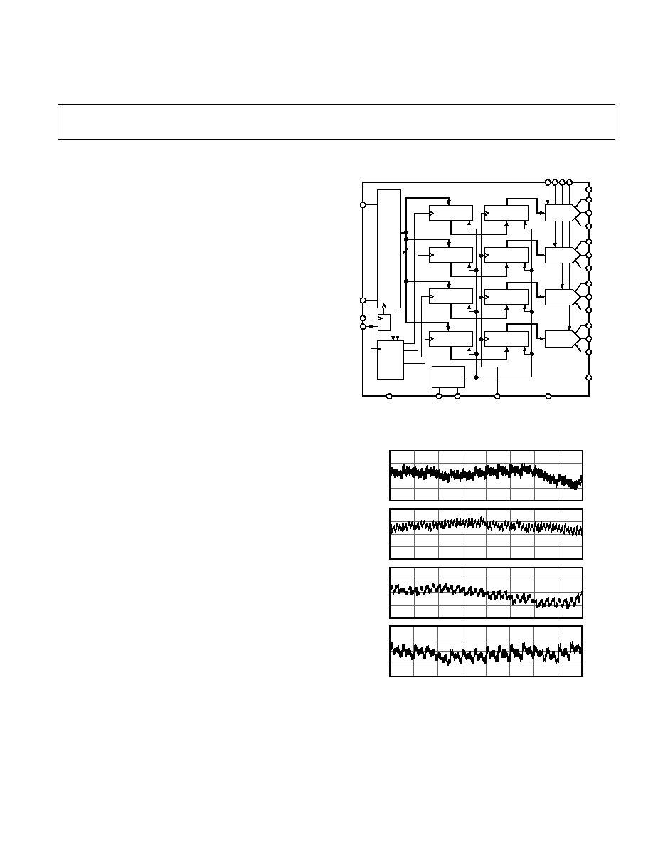
FUNCTIONAL BLOCK DIAGRAM
INPUT
REGISTER R
16
DAC A
REGISTER R
2:4
DECODE
DAC A
B
C
D
POWER-
ON
RESET
D0
D1
D2
D3
D4
D5
D6
D7
D8
D9
D10
D11
D12
D13
D14
D15
A0
A1
DAC B
DAC C
DAC D
DAC A
EN
V
DD
R
FB
A
I
OUT
A
A
GND
A
A
GND
F
V
SS
LDAC
MSB
RS
DGND
CLK
CS
SDI
SDO
V
REF
A B C D
R
FB
B
I
OUT
B
A
GND
B
R
FB
C
I
OUT
C
A
GND
C
R
FB
D
I
OUT
D
A
GND
D
AD5544
INPUT
REGISTER R
INPUT
REGISTER R
INPUT
REGISTER R
DAC B
REGISTER R
DAC C
REGISTER R
DAC D
REGISTER R
FEATURES
AD5544 16-Bit Resolution
AD5554 14-Bit Resolution
2 mA Full-Scale Current 20%, with V
REF
= 10 V
2 s Settling Time
V
SS
BIAS for Zero-Scale Error Reduction @ Temp
Midscale or Zero-Scale Reset
Four Separate 4Q Multiplying Reference Inputs
SPI-Compatible 3-Wire Interface
Double Buffered Registers Enable
Simultaneous Multichannel Change
Internal Power ON Reset
Compact SSOP-28 Package
APPLICATIONS
Automatic Test Equipment
Instrumentation
Digitally-Controlled Calibration
GENERAL DESCRIPTION
The AD5544/AD5554 quad, 16-/14-bit, current-output, digital-
to-analog converters are designed to operate from a single 5 V
supply.
The applied external reference input voltage (V
REF
) determines
the full-scale output current. Integrated feedback resistors (R
FB
)
provide temperature-tracking, full-scale voltage outputs when
combined with an external I-to-V precision amplifier.
A doubled-buffered serial-data interface offers high-speed,
3-wire, SPI- and microcontroller-compatible inputs using
serial-data-in (SDI), clock (CLK), and a chip-select (
CS). In
addition, a serial-data-out pin (SDO) allows for daisy-chaining
when multiple packages are used. A common level-sensitive
load-DAC strobe (
LDAC) input allows simultaneous update of
all DAC outputs from previously loaded input registers. Addi-
tionally, an internal power ON reset forces the output voltage to
zero at system turn ON. An MSB pin allows system reset asser-
tion (
RS) to force all registers to zero code when MSB = 0, or
to half-scale code when MSB = 1.
AD5544/AD5554 are packaged in the compact SSOP-28.
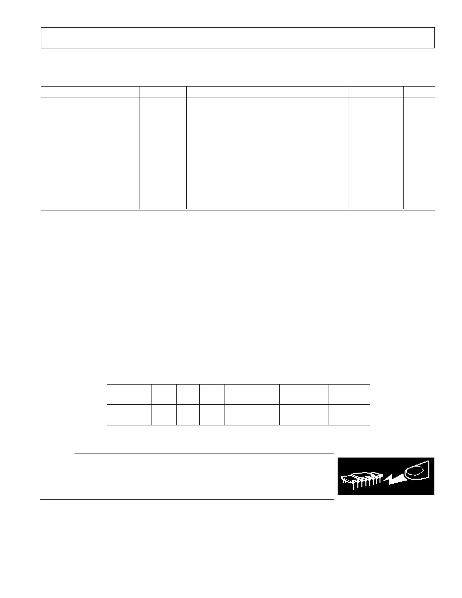
57344
49152
40960
32768
24576
16384
8192
0
65536
CODE ≠ Decimal
1.0
0.5
0.0
≠0.5
≠1.0
1.0
0.5
0.0
≠0.5
≠1.0
1.0
0.5
0.0
≠0.5
≠1.0
1.0
0.5
0.0
≠0.5
≠1.0
INL ≠ LSB
DAC A
DAC B
DAC C
DAC D
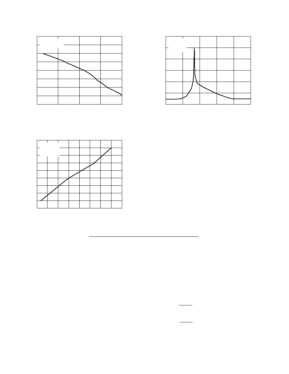
Figure 1. AD5544 INL vs. Code Plot (T
A
= 25
∞C)

REV. 0
≠2≠
AD5544/AD5554≠SPECIFICATIONS
AD5544 ELECTRICAL CHARACTERISTICS
Parameter
Symbol
Condition
Min
Typ
Max
Unit
STATIC PERFORMANCE
1
Resolution
N
1 LSB = V
REF
/2
16
= 153
µV when V
REF
= 10 V
16
Bits
Relative Accuracy
INL
±4
LSB
Differential Nonlinearity
DNL
±1.5
LSB
Output Leakage Current
I
OUT
X
Data = 0000
H
, T
A
= 25
∞C
10
nA
I
OUT
X
Data = 0000
H
, T
A
= T
A
Max
20
nA
Full-Scale Gain Error
G
FSE
Data = FFFF
H
±0.75
±3
mV
Full-Scale Tempco
2
TCV
FS
1
ppm/
∞C
Feedback Resistor
R
FB
X
V
DD
= 5 V
4
6
8
k
REFERENCE INPUT
V
REF
X Range
V
REF
X
≠15
+15
V
Input Resistance
R
REF
X
4
6
8
k
Input Resistance Match
R
REF
X
Channel-to-Channel
1
%
Input Capacitance
2
C
REF
X
5
pF
ANALOG OUTPUT
Output Current
I
OUT
X
Data = FFFF
H
1.25
2.5
mA
Output Capacitance
2
C
OUT
X
Code-Dependent
80
pF
LOGIC INPUTS AND OUTPUT
Logic Input Low Voltage
V
IL
0.8
V
Logic Input High Voltage
V
IH
2.4
V
Input Leakage Current
I
IL
1
µA
Input Capacitance
2
C
IL
10
pF
Logic Output Low Voltage
V
OL
I
OL
= 1.6 mA
0.4
V
Logic Output High Voltage
V
OH
I
OH
= 100
µA
4
V
INTERFACE TIMING
2, 3
Clock Width High
t
CH
25
ns
Clock Width Low
t
CL
25
ns
CS to Clock Setup
t
CSS
0
ns
Clock to
CS Hold
t
CSH
25
ns
Clock to SDO Prop Delay
t
PD
2
20
ns
Load DAC Pulsewidth
t
LDAC
25
ns
Data Setup
t
DS
20
ns
Data Hold
t
DH
20
ns
Load Setup
t
LDS
5
ns
Load Hold
t
LDH
25
ns
SUPPLY CHARACTERISTICS
Power Supply Range
V
DD RANGE
4.5
5.5
V
Positive Supply Current
I
DD
Logic Inputs = 0 V
50
250
µA
Negative Supply Current
I
SS
Logic Inputs = 0 V, V
SS
= ≠5 V
0.001
1
µA
Power Dissipation
P
DISS
Logic Inputs = 0 V
1.25
mW
Power Supply Sensitivity
PSS
V
DD
=
±5%
0.006
%/%
NOTES
1
All static performance tests (except I
OUT
) are performed in a closed-loop system using an external precision OP177 I-to-V converter amplifier. The AD5544
R
FB
terminal is tied to the amplifier output. Typical values represent average readings measured at 25
∞C.
2
These parameters are guaranteed by design and not subject to production testing.
3
All input control signals are specified with t
R
= t
F
= 2.5 ns (10% to 90% of 3 V) and timed from a voltage level of 1.5 V.
Specifications subject to change without notice.
(@ V
DD
= 5 V
10%, V
SS
= 0 V, I
OUT
X = Virtual GND, A
GND
X = 0 V,
V
REF
A, B, C, D = 10 V, T
A
= Full Operating Temperature Range,
unless otherwise noted.)

REV. 0
AD5544/AD5554
≠3≠
AD5544 ELECTRICAL CHARACTERISTICS
Parameter
Symbol
Condition
Min
Typ Max
Unit
AC CHARACTERISTICS
1
Output Voltage Settling Time t
S
To
±0.1% of Full Scale, Data = 0000
H
1
µs
to FFFF
H
to 0000
H
Output Voltage Settling Time t
S
To
±0.0015% of Full Scale, Data = 0000
H
2
µs
to FFFF
H
to 0000
H
Reference Multiplying BW
BW ≠3 dB
V
REF
X = 100 mV rms, Data = FFFF
H
,
2
MHz
C
FB
= 15 pF
DAC Glitch Impulse
Q
V
REF
X = 10 V, Data 0000
H
to 8000
H
to 0000
H
1.2
nV-s
Feedthrough Error
V
OUT
X/V
REF
X Data = 0000
H
, V
REF
X = 100 mV rms, f = 100 kHz
≠65
dB
Crosstalk Error
V
OUT
A/V
REF
B Data = 0000
H
, V
REF
B = 100 mV rms,
≠90
dB
Adjacent Channel, f = 100 kHz
Digital Feedthrough
Q
CS = 1, and f
CLK
= 1 MHz
5
nV-s
Total Harmonic Distortion
THD
V
REF
= 5 V p-p, Data = FFFF
H
, f = 1 kHz
≠90
dB
Output Spot Noise Voltage
e
N
f = 1 kHz, BW = 1 Hz
7
nV/
Hz
NOTES
1
All ac characteristic tests are performed in a closed-loop system using an OP42 I-to-V converter amplifier.
Specifications subject to change without notice.
(@ V
DD
= 5 V 10%, V
SS
= ≠300 mV, I
OUT
X = Virtual GND, A
GND
X = 0 V,
V
REF
A, B, C, D = 10 V, T
A
= full operating temperature range, unless
otherwise noted.)

REV. 0
≠4≠
AD5544/AD5554≠SPECIFICATIONS
AD5554 ELECTRICAL CHARACTERISTICS
Parameter
Symbol
Condition
Min
Typ
Max
Unit
STATIC PERFORMANCE
1
Resolution
N
1 LSB = V
REF
/2
14
= 610
µV when V
REF
= 10 V
14
Bits
Relative Accuracy
INL
±1
LSB
Differential Nonlinearity
DNL
±1
LSB
Output Leakage Current
I
OUT
X
Data = 0000
H
, T
A
= 25
∞C
10
nA
I
OUT
X
Data = 0000
H
, T
A
= T
A
Max
20
nA
Full-Scale Gain Error
G
FSE
Data = 3FFF
H
±2
±10
mV
Full-Scale Tempco
2
TCV
FS
1
ppm/
∞C
Feedback Resistor
R
FB
X
V
DD
= 5 V
4
6
8
k
REFERENCE INPUT
V
REF
X Range
V
REF
X
≠15
+15
V
Input Resistance
R
REF
X
4
6
8
k
Input Resistance Match
R
REF
X
Channel-to-Channel
1
%
Input Capacitance
2
C
REF
X
5
pF
ANALOG OUTPUT
Output Current
I
OUT
X
Data = 3FFF
H
1.25
2.5
mA
Output Capacitance
2
C
OUT
X
Code-Dependent
80
pF
LOGIC INPUTS AND OUTPUT
Logic Input Low Voltage
V
IL
0.8
V
Logic Input High Voltage
V
IH
2.4
V
Input Leakage Current
I
IL
1
µA
Input Capacitance
2
C
IL
10
pF
Logic Output Low Voltage
V
OL
I
OL
= 1.6 mA
0.4
V
Logic Output High Voltage
V
OH
I
OH
= 100
µA
4
V
INTERFACE TIMING
2, 3
Clock Width High
t
CH
25
ns
Clock Width Low
t
CL
25
ns
CS to Clock Setup
t
CSS
0
ns
Clock to
CS Hold
t
CSH
25
ns
Clock to SDO Prop Delay
t
PD
2
20
ns
Load DAC Pulsewidth
t
LDAC
25
ns
Data Setup
t
DS
20
ns
Data Hold
t
DH
20
ns
Load Setup
t
LDS
5
ns
Load Hold
t
LDH
25
ns
SUPPLY CHARACTERISTICS
Power Supply Range
V
DD RANGE
4.5
5.5
V
Positive Supply Current
I
DD
Logic Inputs = 0 V
50
250
µA
Negative Supply Current
I
SS
Logic Inputs = 0 V, V
SS
= ≠5 V
0.001
1
µA
Power Dissipation
P
DISS
Logic Inputs = 0 V
1.25
mW
Power Supply Sensitivity
PSS
V
DD
=
±5%
0.006
%/%
NOTES:
1
All static performance tests (except I
OUT
) are performed in a closed-loop system using an external precision OP177 I-to-V converter amplifier. The AD5554
R
FB
terminal is tied to the amplifier output. Typical values represent average readings measured at 25
∞C.
2
These parameters are guaranteed by design and not subject to production testing.
3
All input control signals are specified with t
R
= t
F
= 2.5 ns (10% to 90% of 3 V) and timed from a voltage level of 1.5 V.
Specifications subject to change without notice.
(@ V
DD
= 5 V 10%, V
SS
= 0 V, I
OUT
X = Virtual GND, A
GND
X = 0 V,
V
REF
A, B, C, D = 10 V, T
A
= full operating temperature range,
unless otherwise noted.)
REV. 0
AD5544/AD5554
≠5≠
AD5554 ELECTRICAL CHARACTERISTICS
Parameter
Symbol
Condition
Min Typ Max
Unit
AC CHARACTERISTICS
1
Output Voltage Settling Time t
S
To
±0.1% of Full Scale, Data = 0000
H
1
µs
to 3FFF
H
to 0000
H
Output Voltage Settling Time t
S
To
±0.0015% of Full Scale, Data = 0000
H
2
µs
to 3FFF
H
to 0000
H
Reference Multiplying BW
BW ≠3 dB
V
REF
X = 100 mV rms, Data = 3FFF
H
, C
FB
= 15 pF
2
MHz
DAC Glitch Impulse
Q
V
REF
X = 10 V, Data 0000
H
to 2000
H
to 0000
H
1.2
nV-s
Feedthrough Error
V
OUT
X/V
REF
X Data = 0000
H
, V
REF
X = 100 mV rms, f = 100 kHz
≠65
dB
Crosstalk Error
V
OUT
A/V
REF
B Data = 0000
H
, V
REF
B = 100 mV rms,
Adjacent Channel, f = 100 kHz
≠90
dB
Digital Feedthrough
Q
CS = 1, and f
CLK
= 1 MHz
5
nV-s
Total Harmonic Distortion
THD
V
REF
= 5 V p-p, Data = 3FFF
H
, f = 1 kHz
≠90
dB
Output Spot Noise Voltage
e
N
f = 1 kHz, BW = 1 Hz
7
nV/
Hz
NOTES:
1
All ac characteristic tests are performed in a closed-loop system using an OP42 I-to-V converter amplifier.
Specifications subject to change without notice.
(@ V
DD
= 5 V 10%, V
SS
= ≠300 mV, I
OUT
X = Virtual GND, A
GND
X = 0 V, V
REF
A,
B, C, D = 10 V, T
A
= full operating temperature range, unless otherwise
noted.)
ABSOLUTE MAXIMUM RATINGS
*
V
DD
to GND . . . . . . . . . . . . . . . . . . . . . . . . . . . . ≠0.3 V, +8 V
V
SS
to GND . . . . . . . . . . . . . . . . . . . . . . . . . . . . . +0.3 V, ≠7 V
V
REF
to GND . . . . . . . . . . . . . . . . . . . . . . . . . . . . ≠18 V, +18 V
Logic Inputs and Output to GND . . . . . . . . . . . . ≠0.3 V, +8 V
V(I
OUT
) to GND . . . . . . . . . . . . . . . . . . . . ≠0.3 V, V
DD
+ 0.3 V
A
GND
X to DGND . . . . . . . . . . . . . . . . . . . . . . ≠0.3 V, + 0.3 V
Input Current to Any Pin Except Supplies . . . . . . . . .
±50 mA
Package Power Dissipation . . . . . . . . . . . . (T
J
MAX ≠ T
A
)/
JA
Thermal Resistance
JA
28-Lead Shrink Surface-Mount (RS-28) . . . . . . . . 100
∞C/W
Maximum Junction Temperature (T
J
MAX) . . . . . . . . . 150
∞C
CAUTION
ESD (electrostatic discharge) sensitive device. Electrostatic charges as high as 4000 V readily
accumulate on the human body and test equipment and can discharge without detection. Although
the AD5544/AD5554 features proprietary ESD protection circuitry, permanent damage may occur
on devices subjected to high-energy electrostatic discharges. Therefore, proper ESD precautions
are recommended to avoid performance degradation or loss of functionality.
WARNING!
ESD SENSITIVE DEVICE
ORDERING GUIDE
RES
INL
DNL
Temperature
Package
Package
Model
Bit
LSB
LSB
Range
Description
Option
AD5544ARS
16
±4
±1.5
≠40/+85
∞C
SSOP-28
RS-28
AD5554BRS
14
±1
±1
≠40/+85
∞C
SSOP-28
RS-28
The AD5544/AD5554 contain 4196 transistors. The die size is 122 mil
◊ 204 mil.
Operating Temperature Range
Model A . . . . . . . . . . . . . . . . . . . . . . . . . . . ≠40
∞C to +85∞C
Storage Temperature Range . . . . . . . . . . . . . ≠65
∞C to +150∞C
Lead Temperature:
RS-28 (Vapor Phase, 60 secs) . . . . . . . . . . . . . . . . . . 215
∞C
RS-28 (Infrared, 15 secs) . . . . . . . . . . . . . . . . . . . . . . 220
∞C
*Stresses above those listed under Absolute Maximum Ratings may cause perma-
nent damage to the device. This is a stress rating only; functional operation of the
device at these or any other conditions above those indicated in the operational
sections of this specification is not implied. Exposure to absolute maximum rating
conditions for extended periods may affect device reliability.
REV. 0
AD5544/AD5554
≠6≠
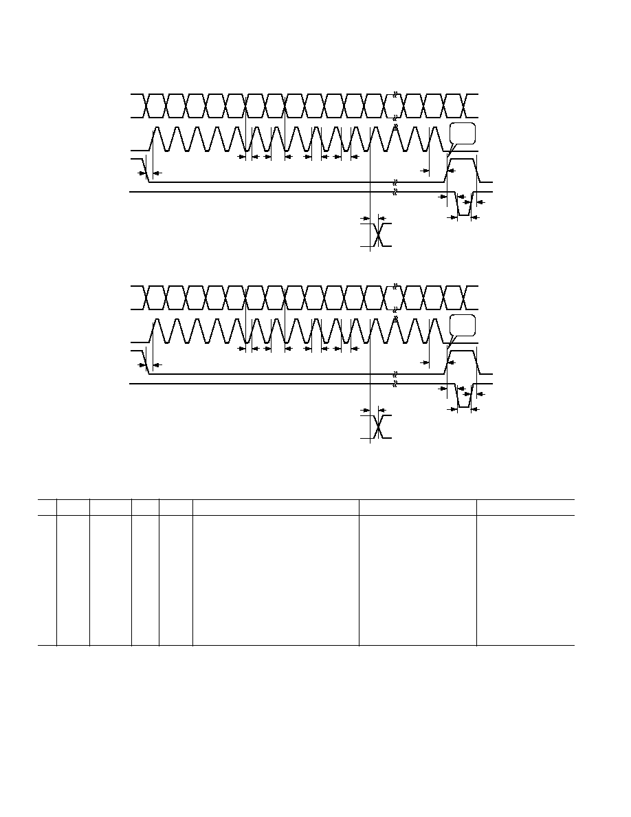
t
LDH
t
LDS
t
LDAC
t
CSH
t
PD
t
CL
t
CH
t
DH
t
DS
t
CSS
SDI
CLK
CS
LDAC
SDO
INPUT
REG
LD
A1
A0
D15
D14
D13
D12
D11
D10
D1
D0
Figure 2. AD5544 Timing Diagram
t
LDH
t
LDS
t
LDAC
t
CSH
t
PD
t
CL
t
CH
t
DH
t
DS
t
CSS
SDI
CLK
CS
LDAC
SDO
INPUT
REG
LD
A1
A0
D13
D12
D11
D10
D09
D08
D1
D0
Figure 3. AD5554 Timing Diagram
Table I. AD5544 Control-Logic Truth Table
CS
CLK
LDAC
RS
MSB
Serial Shift Register Function
Input Register Function
DAC Register
H
X
H
H
X
No Effect
Latched
Latched
L
L
H
H
X
No Effect
Latched
Latched
L
+
H
H
X
Shift-Register-Data Advanced One Bit
Latched
Latched
L
H
H
H
X
No Effect
Latched
Latched
+
L
H
H
X
No Effect
Selected DAC Updated
Latched
with Current SR Contents
H
X
L
H
X
No Effect
Latched
Transparent
H
X
H
H
X
No Effect
Latched
Latched
H
X
+
H
X
No Effect
Latched
Latched
H
X
H
L
0
No Effect
Latched Data = 0000
H
Latched Data = 0000
H
H
X
H
L
H
No Effect
Latched Data = 8000
H
Latched Data = 8000
H
REV. 0
AD5544/AD5554
≠7≠
Table II. AD5554 Control-Logic Truth Table
CS
CLK
LDAC
RS
MSB
Serial Shift Register Function
Input Register Function
DAC Register
H
X
H
H
X
No Effect
Latched
Latched
L
L
H
H
X
No Effect
Latched
Latched
L
+
H
H
X
Shift-Register-Data Advanced One Bit
Latched
Latched
L
H
H
H
X
No Effect
Latched
Latched
+
L
H
H
X
No Effect
Selected DAC Updated
Latched
with Current SR Contents
H
X
L
H
X
No Effect
Latched
Transparent
H
X
H
H
X
No Effect
Latched
Latched
H
X
+
H
X
No Effect
Latched
Latched
H
X
H
L
0
No Effect
Latched Data = 0000
H
Latched Data = 0000
H
H
X
H
L
H
No Effect
Latched Data = 2000
H
Latched Data = 2000
H
NOTES
1. SR = Shift Register.
2.
+ positive logic transition; X = Don't Care.
3. At power ON both the Input Register and the DAC Register are loaded with all zeros.
4. For AD5544, data appears at the SDO Pin 19 clock pulses after input at the SDI pin.
5. For AD5554, data appears at the SDO Pin 17 clock pulses after input at the SDI pin.
Table III. AD5544 Serial Input Register Data Format, Data Is Loaded in the MSB-First Format
MSB
LSB
Bit Position B17
B16
B15
B14
B13
B12
B11
B10
B9
B8
B7
B6
B5
B4
B3
B2
B1 B0
Data Word A1
A0
D15
D14
D13
D12
D11
D10
D9
D8
D7
D6
D5
D4
D3
D2
D1 D0
NOTE
Only the last 18 bits of data clocked into the serial register (Address + Data) are inspected when the
CS line's positive edge returns to logic high. At this point an inter-
nally generated load strobe transfers the serial register data contents (Bits D15≠D0) to the decoded DAC-Input-Register address determined by bits A1 and A0. Any
extra bits clocked into the AD5544 shift register are ignored, only the last 18 bits clocked in are used. If double-buffered data is not needed, the
LDAC pin can be tied
logic low to disable the DAC Registers.
Table IV. AD5554 Serial Input Register Data Format, Data Is Loaded in the MSB-First Format
MSB
LSB
Bit Position B15
B14
B13
B12
B11
B10
B9
B8
B7
B6
B5
B4
B3
B2
B1
B0
Data Word
A1
A0
D13
D12
D11
D10
D9
D8
D7
D6
D5
D4
D3
D2
D1
D0
NOTE
Only the last 16 bits of data clocked into the serial register (Address + Data) are inspected when the
CS line's positive edge returns to logic high. At this point an inter-
nally generated load strobe transfers the serial register data contents (Bits D13≠D0) to the decoded DAC-Input-Register address determined by bits A1 and A0. Any
extra bits clocked into the AD5554 shift register are ignored, only the last 16 bits clocked in are used. If double-buffered data is not needed, the
LDAC pin can be tied
logic low to disable the DAC Registers.
Table V. Address Decode
A1
A0
DAC Decoded
0
0
DAC A
0
1
DAC B
1
0
DAC C
1
1
DAC D
REV. 0
AD5544/AD5554
≠8≠
AD5544/AD5554 PIN FUNCTION DESCRIPTIONS
Pin # Name
Function
1
A
GND
A
DAC A Analog Ground.
2
I
OUT
A
DAC A Current Output.
3
V
REF
A
DAC A Reference Voltage Input Terminal. Establishes DAC A full-scale output voltage. Pin can be tied to V
DD
pin.
4
R
FB
A
Establish Voltage Output for DAC A by Connecting to External Amplifier Output.
5
MSB
MSB Bit Set Pin During a Reset Pulse (
RS) or at System Power ON if Tied to Ground or V
DD
.
6
RS
Reset Pin, Active Low Input. Input registers and DAC registers are set to all zeros or half-scale code (8000
H
for
AD5544 and 2000
H
for AD5554) determined by the voltage on the MSB pin. Register Data = 0000
H
when MSB
= 0. Register Data = 8000
H
for AD5544 and 2000
H
for AD5554 when MSB = 1.
7
V
DD
Positive Power Supply Input. Specified range of operation 5 V
± 10%.
8
CS
Chip Select, Active Low Input. Disables shift register loading when high. Transfers serial register data to the Input
Register when
CS/LDAC returns High. Does not effect LDAC operation.
9
CLK
Clock Input, Positive Edge Clocks Data into Shift Register.
10
SDI
Serial Data Input, Input Data Loads Directly into the Shift Register.
11
R
FB
B
Establish Voltage Output for DAC B by Connecting to External Amplifier Output.
12
V
REF
B
DAC B Reference Voltage Input Terminal. Establishes DAC B full-scale output voltage. Pin can be tied to V
DD
pin.
13
I
OUT
B
DAC B Current Output.
14
A
GND
B
DAC B Analog Ground.
15
A
GND
C
DAC C Analog Ground.
16
I
OUT
C
DAC C Current Output.
17
V
REF
C
DAC C Reference Voltage Input Terminal. Establishes DAC C full-scale output voltage. Pin can be tied to V
DD
pin.
18
R
FB
C
Establish voltage output for DAC C by connecting to external amplifier output.
19
NC
No Connect. Leave pin unconnected.
20
SDO
Serial Data Output, input data loads directly into the shift register. Data appears at SDO, 19 clock pulses for
AD5544 and 17 clock pulses for AD5554 after input at the SDI pin.
21
LDAC
Load DAC Register Strobe, Level Sensitive Active Low. Transfers all Input Register data to DAC registers. Asyn-
chronous active low input. See Control Logic Truth Table for operation.
22
A
GND
F
High Current Analog Force Ground.
23
V
SS
Negative Bias Power Supply Input. Specified range of operation ≠0.3 V to ≠5.5 V.
24
DGND
Digital Ground Pin.
25
R
FB
D
Establish Voltage Output for DAC D by Connecting to External Amplifier Output.
26
V
REF
D
DAC D Reference Voltage Input Terminal. Establishes DAC D full-scale output voltage. Pin can be tied to V
DD
pin.
27
I
OUT
D
DAC D Current Output.
28
A
GND
D
DAC D Analog Ground.
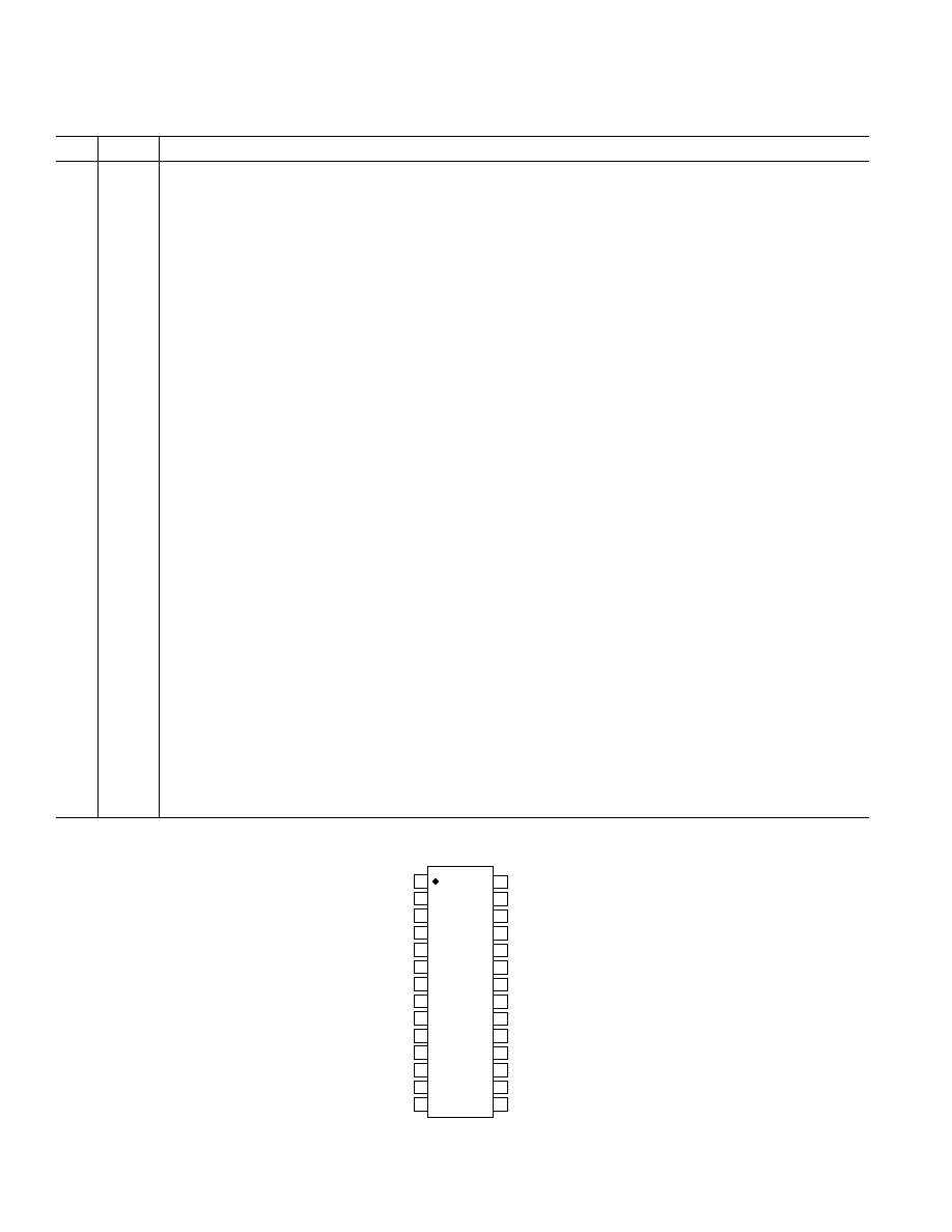
AD5544/AD5554 PIN CONFIGURATION
TOP VIEW
(Not to Scale)
28
27
26
25
24
23
22
21
20
19
18
17
16
15
1
2
3
4
5
6
7
8
9
10
11
12
13
14
AD5544/
AD5554
A
GND
A
A
GND
D
I
OUT
A
I
OUT
D
V
REF
A
V
REF
D
R
FB
A
R
FB
D
MSB
DGND
RS
V
SS
V
DD
A
GND
F
CS
LDAC
CLK
SDO
SDI
NC
R
FB
B
R
FB
C
V
REF
B
V
REF
C
I
OUT
B
I
OUT
C
A
GND
B
A
GND
C
NC = NO CONNECT
REV. 0
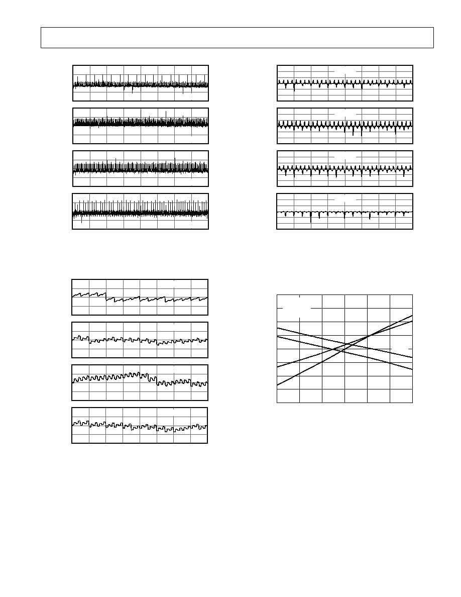
Typical Performance Characteristics≠AD5544/AD5554
≠9≠
57344
49152
40960
32768
24576
16384
8192
0
65536
CODE ≠ Decimal
0.50
0.25
0.00
≠0.25
≠0.50
DAC D
DAC A
DAC C
0.50
0.25
0.00
≠0.25
≠0.50
DAC B
0.50
0.25
0.00
≠0.25
≠0.50
DNL
≠
LSB
0.50
0.25
0.00
≠0.25
≠0.50
TPC 1. AD5544 DNL vs. Code (T
A
= 25
∞C)
14336
12288
10240
8192
6144
4096
2048
0
16384
CODE ≠ Decimal
DAC D
DAC A
DAC C
DAC B
INL
≠
LSB
1.0
0.5
0.0
≠0.5
≠1.0
1.0
0.5
0.0
≠0.5
≠1.0
1.0
0.5
0.0
≠0.5
≠1.0
1.0
0.5
0.0
≠0.5
≠1.0
TPC 2. AD5554 INL vs. Code (T
A
= 25
∞C)
14336
12288
10240
8192
6144
4096
2048
0
16384
CODE ≠ Decimal
DAC D
DAC A
DAC C
DAC B
DNL
≠
LSB
0.75
0.50
0.25
0.00
≠0.25
≠0.50
≠0.75
0.75
0.50
0.25
0.00
≠0.25
≠0.50
≠0.75
0.75
0.50
0.25
0.00
≠0.25
≠0.50
≠0.75
0.75
0.50
0.25
0.00
≠0.25
≠0.50
≠0.75
TPC 3. AD5554 DNL vs. Code (T
A
= 25
∞C)
OP AMP OFFSET VOLTAGE ≠ V
2.0
INTEGRAL NONLINEARITY ERROR
≠
LSB
≠1500
1.5
1.0
0.5
0
≠0.5
≠1.0
≠1.5
≠2.0
≠1000
≠500
0
500
1000
1500
V
DD
= 5V
V
REF
= 10V
T
A
= 25 C
F000
H
8000
H
0FFF
H
7FFF
H
TPC 4. AD5544 Integral Nonlinearity Error vs.
Op Amp Offset
REV. 0
AD5544/AD5554
≠10≠
OP AMP OFFSET VOLTAGE ≠ V
0.75
INTEGRAL NONLINEARITY ERROR
≠
LSB
≠2000
0.50
0.25
0.00
≠0.25
≠0.50
≠0.75
≠1500
≠1000
≠500
0
500
2000
1000
1500
1FFF
H
2000
H
3000
H
0FFF
H
V
DD
= 5V
V
REF
= 10V
T
A
= 25 C
TPC 5. AD5554 Integral Nonlinearity Error vs.
Op Amp Offset
OP AMP OFFSET VOLTAGE ≠ V
1.00
DIFFERENTIAL NONLINEARITY ERROR
≠
LSB
≠1000
0.75
0.50
0.25
0.00
≠0.25
≠0.50
≠0.75
≠1.00
≠750
≠500
≠250
0
250
500
750
1000
V
DD
= 5V
V
REF
= 10V
T
A
= 25 C
8000
H
F000
H
0FFF
H
TPC 6. AD5544 Differential Nonlinearity Error vs.
Op Amp Offset
OP AMP OFFSET VOLTAGE ≠ V
0.3
DIFFERENTIAL NONLINEARITY ERROR
≠
LSB
≠1500
0.2
0.1
0.0
≠0.1
≠0.2
≠0.3
≠1000
≠500
0
500
1500
1000
V
DD
= 5V
V
REF
= 10V
T
A
= 25 C
2000
H
3000
H
0FFF
H
ACCURACY DEGRADATION
DUE TO EXTERNAL OP AMP
INPUT OFFSET VOLTAGE
SPECIFICATION.
TPC 7. AD5554 Differential Nonlinearity Error vs.
Op Amp Offset
OP AMP OFFSET VOLTAGE ≠ V
10.0
GAIN ERROR
≠
LSB
≠1500
7.5
5.0
2.5
0.0
≠2.5
≠5.0
≠1000
≠500
0
500
1000
1500
V
DD
= 5V
V
REF
= 10V
T
A
= 25 C
≠7.5
≠10.0
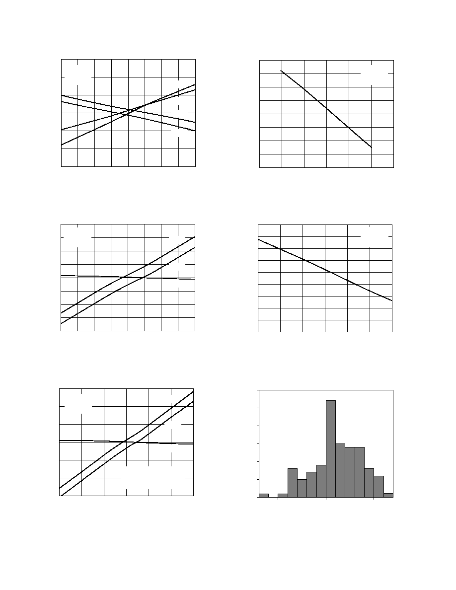
TPC 8. AD5544 Gain Error vs. Op Amp Offset
OP AMP OFFSET VOLTAGE ≠ V
4
GAIN ERROR
≠
LSB
≠1500
3
2
1
0
≠1
≠2
≠3
≠5
≠1000
≠500
0
500
1000
1500
≠4
V
DD
= 5V
V
REF
= 10V
T
A
= 25 C
TPC 9. AD5554 Gain Error vs. Op Amp Offset
FULL-SCALE TEMPCO ≠ ppm/ C
30
FREQUENCY
0
20
10
0
0.5
1.0
1.5
SS = 120 UNITS
V
DD
= 5V
V
REF
= 10V
T
A
= ≠40 C TO +85 C
TPC 10. AD5544 Full-Scale Tempco (ppm/ C)
REV. 0
AD5544/AD5554
≠11≠
FULL-SCALE ERROR TEMPCO ≠ ppm/ C
40
FREQUENCY
0.2
30
20
10
0.4
0.6
0.8
1.0
1.2
1.4
1.6
1.8
0
60
SS = 180 UNITS
V
DD
= 5V
V
REF
= 10V
T
A
= ≠40 C TO +85 C
TPC 11. AD5554 Full-Scale Tempco (ppm/ C)
100ns/DIV
CS
(5V/DIV)
V
OUT
(50mV/DIV)
V
DD
= 5V
V
REF
= 10V
T
A
= 25 C
7FFF
H
8000
H
TPC 12. AD5544 Midscale Transition
2 s/DIV
CS
(5V/DIV)
V
OUT
(5V/DIV)
V
DD
= 5V
V
REF
= 10V
T
A
= 25 C
0000
H
FFFF
H
TPC 13. AD5544 Large Signal Settling Time
1 s/DIV
V
OUT
(10V/DIV)
V
OUT
(50mV/DIV)
V
DD
= 5V
V
REF
= 10V
T
A
= 25 C
A
V
= ≠343
1LSB = 52mV
TPC 14. AD5544 Small Signal Settling Time
CLOCK FREQUENCY ≠ Hz
10000
1k
I
DD
≠
A
1000
100
10
10k
100k
1M
10M
100M
V
DD
= 5V
V
REF
= 10V
T
A
= 25 C
5555
H
FFFF
H
8000
H
0000
H
TPC 15. AD5544 Power Supply Current vs.
Clock Frequency
CLOCK FREQUENCY ≠ Hz
10000
1k
I
DD
≠
A
1000
100
10
10k
100k
1M
10M
100M
V
DD
= 5V
V
REF
= 10V
T
A
= 25 C
1555
H
3FFF
H
2000
H
0000
H
TPC 16. AD5554 Power Supply Current vs.
Clock Frequency
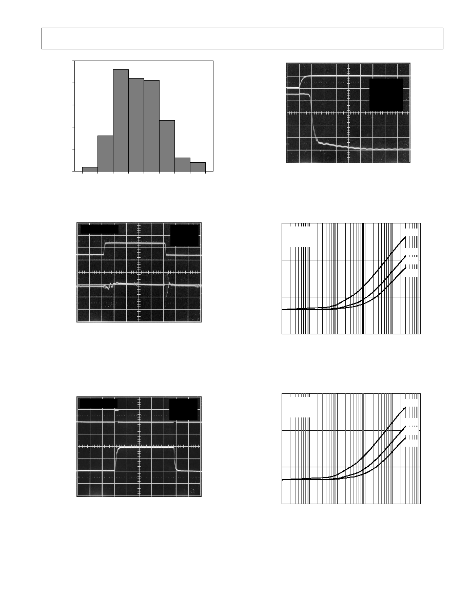
REV. 0
AD5544/AD5554
≠12≠
CLOCK FREQUENCY ≠ Hz
100
1k
PSRR
≠
dB
10k
100k
1M
100
V
DD
= 5V 10%
T
A
= 25 C
90
80
70
60
50
40
30
20
TPC 17. AD5544/AD5554 Power Supply Rejection
vs. Frequency
TEMPERATURE ≠ C
55
SUPPLY CURRENT
≠
A
≠50
V
DD
= 5V
V
REF
= 10V
LOGIC = V
DD
54
53
52
51
50
49
48
47
46
≠25
0
25
50
75
100
125
150
TPC 18. AD5544/AD5554 Power Supply Current
vs. Temperature
LOGIC INPUT VOLTAGE ≠ Volts
600
I
DD
≠
A
0
V
DD
= 5V
V
REF
= 10V
T
A
= 25 C
500
400
300
200
100
0
1
2
3
4
5
TPC 19. AD5544/AD5554 Power Supply Current
vs. Logic Input Voltage
CIRCUIT OPERATION
The AD5544 and AD5554 contain four, 16-bit and 14-bit,
current-output, digital-to-analog converters respectively. Each
DAC has its own independent multiplying reference input. Both
AD5544/AD5554 use 3-wire SPI compatible serial data inter-
face, with a configurable asynchronous
RS pin for half-scale
(MSB = 1) or zero-scale (MSB = 0) preset. In addition, an
LDAC strobe enables four channel simultaneous updates for
hardware synchronized output voltage changes.
D/A Converter Section
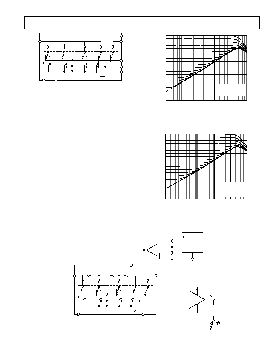
Each part contains four current-steering R-2R ladder DACs.
Figure 4 shows a typical equivalent DAC. Each DAC contains
a matching feedback resistor for use with an external I-to-V
converter amplifier. The R
FB
X pin is connected to the output of
the external amplifier. The I
OUT
X terminal is connected to the
inverting input of the external amplifier. The A
GND
X pin should
be Kelvin-connected to the load point in the circuit requiring
the full 16-bit accuracy. These DACs are designed to operate
with both negative or positive reference voltages. The V
DD
power
pin is only used by the logic to drive the DAC switches ON and
OFF. Note that a matching switch is used in series with the
internal 5 k
feedback resistor. If users are attempting to mea-
sure the value of R
FB
, power must be applied to V
DD
in order to
achieve continuity. An additional V
SS
bias pin is used to guard
the substrate during high temperature applications to minimize
zero-scale leakage currents that double every 10
∞C. The DAC
output voltage is determined by V
REF
and the digital data (D) as:
V
V
OUT
REF
= -
◊
D
65536
(For AD5544)
(Equation 1)
V
V
OUT
REF
= -
◊
D
16384
(For AD5554)
(Equation 2)
Note that the output polarity is opposite to the V
REF
polarity for
dc reference voltages.
REV. 0
AD5544/AD5554
≠13≠
V
REF
X
V
SS
DGND
V
DD
R
FB
X
I
OUT
X
A
GND
F
A
GND
X
R
R
R
R
2R
2R
2R
5k
S1
S2
FROM OTHER DACS A
GND
DIGITAL INTERFACE CONNECTIONS OMITTED FOR CLARITY.
SWITCHES S1 AND S2 ARE CLOSED, V
DD
MUST BE POWERED.
Figure 4. Typical Equivalent DAC Channel
These DACs are also designed to accommodate ac reference
input signals. Both AD5544/AD5554 will accommodate input
reference voltages in the range of ≠12 V to +12 V. The reference
voltage inputs exhibit a constant nominal input resistance of
5 k
, ± 30%. On the other hand, the DAC outputs I
OUT
A, B,
C, D are code-dependent and produce various output resis-
tances and capacitances. The choice of external amplifier
should take into account the variation in impedance generated
by the AD5544/AD5554 on the amplifiers' inverting input
node. The feedback resistance, in parallel with the DAC ladder
resistance, dominates output voltage noise. For multiplying
mode applications, an external feedback compensation capacitor
(C
FB
) may be needed to provide a critically damped output
response for step changes in reference input voltages. Figures 5
and 6 show the gain vs. frequency performance at various
attenuation settings using a 23 pF external feedback capacitor
connected across the I
OUT
X and R
FB
X terminals for AD5544
and AD5554 respectively. In order to maintain good analog
performance, power supply bypassing of 0.01
µF, in parallel
with 1
µF, is recommended. Under these conditions, clean
power supply with low ripple voltage capability should be used.
Switching power supplies is usually not suitable for this application
due to the higher ripple voltage and PSS frequency-dependent
characteristics. It is best to derive the AD5544/AD5554's 5 V
supply from the systems' analog supply voltages. (Do not use
the digital 5 V supply.) See Figure 7.
FREQUENCY ≠ Hz
1k
GAIN
≠
12dB/DIV
FFFF
H
10k
100k
1M
10M
100
B15
B14
B13
B12
B11
B10
B9
B8
B7
B6
B5
B4
B3
B2
ZS
V
DD
= 5V
V
REF
= 100mV rms
T
A
= 25 C
B1
B0
Figure 5. AD5554 Reference Multiplying Bandwidth
vs. Code
FREQUENCY ≠ Hz
1k
GAIN
≠
12dB/DIV
3FFF
H
10k
100k
1M
10M
100
B13
B12
B11
B10
B9
B8
B7
B6
B5
B4
B3
B2
B1
B0
ZS
V
DD
= 5V
V
REF
= 100mV rms
T
A
= 25 C
C
F
= 23pF
Figure 6. AD5554 Reference Multiplying Bandwidth
vs. Code
V
REF
X
V
SS
DGND
V
DD
R
FB
X
I
OUT
X
A
GND
F
A
GND
X
R
R
R
R
2R
2R
2R
5k
S1
S2
FROM OTHER DACS A
GND
AD5544
+
A1
15V
V
EE
V
CC
V
OUT
LOAD
2R
R
5V
15V
ANALOG
POWER
SUPPLY
DIGITAL INTERFACE CONNECTIONS OMITTED.
FOR CLARITY SWITCHES S1 AND S2 ARE CLOSED,
V
DD
MUST BE POWERED.
+
Figure 7. Recommended Kelvin-Sensed Hookup
REV. 0
AD5544/AD5554
≠14≠
SERIAL DATA INTERFACE
The AD5544/AD5554 uses a 3-wire (
CS, SDI, CLK) SPI com-
patible serial data interface. Serial data of AD5544 and AD5554
is clocked into the serial input register in an 18-bit and 16-bit
data-word format respectively. MSB bits are loaded first. Table
II defines the 18 data-word bits for AD5544. Table III defines
the 16 data-word bits for AD5554. Data is placed on the SDI
pin, and clocked into the register on the positive clock edge of
CLK subject to the data setup and data hold time requirements
specified in the Interface Timing Specifications. Data can only
be clocked in while the
CS chip select pin is active low. For
AD5544, only the last 18 bits clocked into the serial register will
be interrogated when the
CS pin returns to the logic high state,
extra data bits are ignored. For AD5554, only the last 16 bits
clocked into the serial register will be interrogated when the
CS
pin returns to the logic high state. Since most microcontrollers
output serial data in 8-bit bytes, three right-justified data bytes
can be written to the AD5544. Keeping the
CS line low between
the first, second, and third byte transfers will result in a success-
ful serial register update. Similarly, two right-justified data bytes
can be written to the AD5554. Keeping the
CS line low between
the first and second byte transfer will result in a successful serial
register update.
Once the data is properly aligned in the shift register, the posi-
tive edge of the
CS initiates the transfer of new data to the target
DAC register, determined by the decoding of address bits A1
and A0. For AD5544, Tables I, III, V, and Figure 2 define the
characteristics of the software serial interface. For AD5554,
Tables II, IV, V, and Figure 3 define the characteristics of the
software serial interface. Figures 8 and 9 show the equivalent
logic interface for the key digital control pins for AD5544.
AD5554 has similar configuration, except with 14 data bits.
Two additional pins
RS and MSB provide hardware control
over the preset function and DAC Register loading. If these
functions are not needed, the
RS pin can be tied to logic high.
The asynchronous input
RS pin forces all input and DAC regis-
ters to either the zero-code state (MSB = 0), or the half-scale
state (MSB = 1)
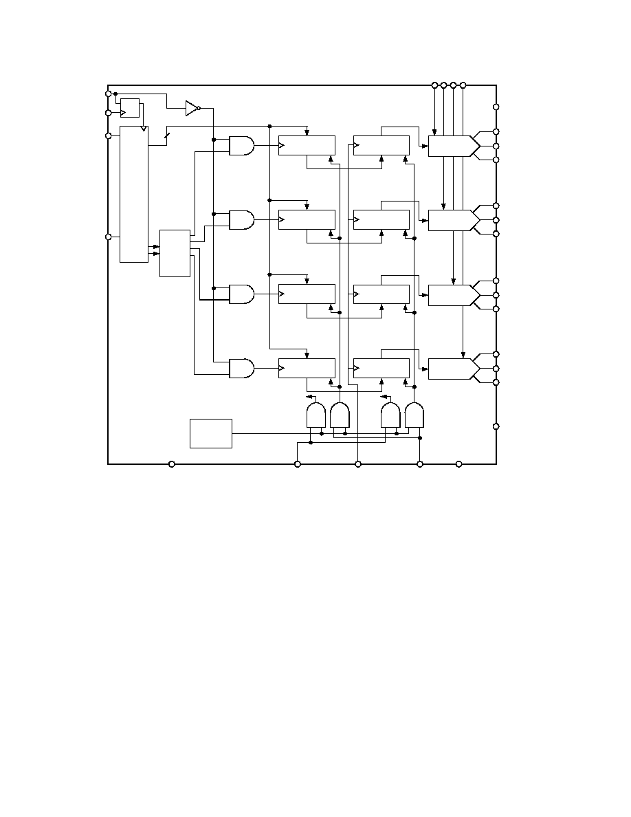
INPUT
REGISTER
R
INPUT
REGISTER
R
INPUT
REGISTER
R
INPUT
REGISTER
R
DAC A
B
C
D
2:4
DECODE
D0
D1
D2
D3
D4
D5
D6
D7
D8
D9
D10
D11
D12
D13
D14
D15
A0
A1
EN
16
DAC D
REGISTER
R
DAC C
REGISTER
R
DAC B
REGISTER
R
DAC A
REGISTER
R
POWER-
ON
RESET
DAC B
DAC C
DAC D
DAC A
AD5544
V
REF
A B C D
V
DD
R
FB
A
I
OUT
A
A
GND
A
R
FB
B
I
OUT
B
A
GND
B
R
FB
C
I
OUT
C
A
GND
C
R
FB
D
I
OUT
D
A
GND
D
A
GND
F
DGND
MSB
LDAC
RS
V
SS
SET
MSB
SET
MSB
SDO
SDI
CLK
CS
Figure 8. System Level Digital Interfacing
REV. 0
AD5544/AD5554
≠15≠
EN
SHIFT REGISTER
ADDRESS
DECODER
A
B
C
D
TO INPUT REGISTER
19
TH
/17
TH
CLOCK
SDO
SDI
CLK
CS
Figure 9. AD5544/AD5554 Equivalent Logic Interface
POWER-ON RESET
When the V
DD
power supply is turned ON, an internal reset
strobe forces all the Input and DAC registers to the zero-code
state or half-scale, depending on the MSB pin voltage. The V
DD
power supply should have a smooth positive ramp without
drooping in order to have consistent results, especially in the
region of V
DD
= 1.5 V to 2.3 V. The V
SS
supply has no effect on
the power-ON reset performance. The DAC register data will
stay at zero or half-scale setting until a valid serial register data
load takes place.
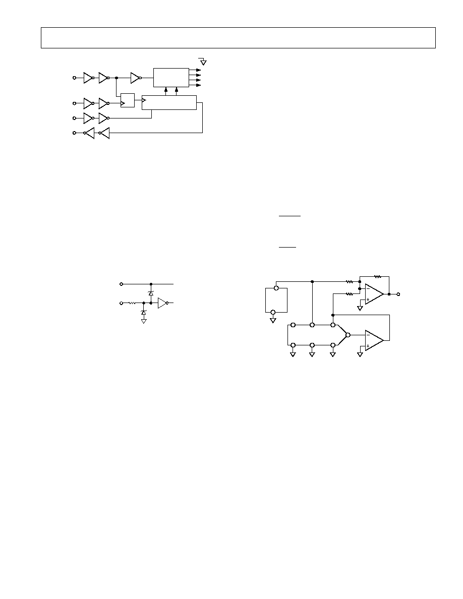
ESD Protection Circuits
All logic-input pins contain back-biased ESD protection Zeners
connected to ground (DGND) and V
DD
as shown in Figure 9.
V
DD
DIGITAL
INPUTS
5k
DGND
Figure 10. Equivalent ESD Protection Circuits
PCB LAYOUT
In PCB layout, all analog ground, A
GND
X, should be tied together.
Amplifiers suitable for I-to-V conversion include:
∑ High Accuracy: OP97, OP297
∑ Speed and Accuracy: OP42
∑
±5 V Applications: OP162/OP262/OP462, OP184/OP284/
OP484
APPLICATIONS
The AD5544/AD5554 are inherently 2-quadrant multiplying
D/A converters. That is, they can be easily set up for unipolar
output operation. The full-scale output polarity is the inverse of
the reference-input voltage.
In some applications it may be necessary to generate the full 4-
quadrant multiplying capability or a bipolar output swing. This
is easily accomplished using an additional external amplifier
(A2) configured as a summing amplifier (see Figure 11). In this
circuit the first and second amplifiers (A1 and A2) provide a
total gain-of-2 which increases the output voltage span to 20 V.
Biasing the external amplifier with a 10 V offset from the refer-
ence voltage results in a full 4-quadrant multiplying circuit. The
transfer equation of this circuit shows that both negative and
positive output voltages are created as the input data (D) is
incremented from code zero (V
OUT
= ≠10 V) to midscale (V
OUT
= 0 V) to full-scale (V
OUT
= 10 V).
V
D
V
OUT
REF
=
-
◊
32768
1
(For AD5544)
(Equation 3)
V
D
V
OUT
REF
=
-
◊
8192
1
(For AD5554)
(Equation 4)
A2
A1
ONE CHANNEL
AD5544
I
OUT
X
R
FB
X
V
REF
X
V
DD
V
SS
A
GND
F
A
GND
X
V
OUT
10k
10k
5k
AD588
V
REF
10V
DIGITAL INTERFACE CONNECTIONS
OMITTED FOR CLARITY.
≠10V < V
OUT
< +10V
Figure 11. Four-Quadrant Multiplying Application Circuit
REV. 0
≠16≠
C3563≠8≠4/00 (rev. 0) 00943
PRINTED IN U.S.A.
AD5544/AD5554
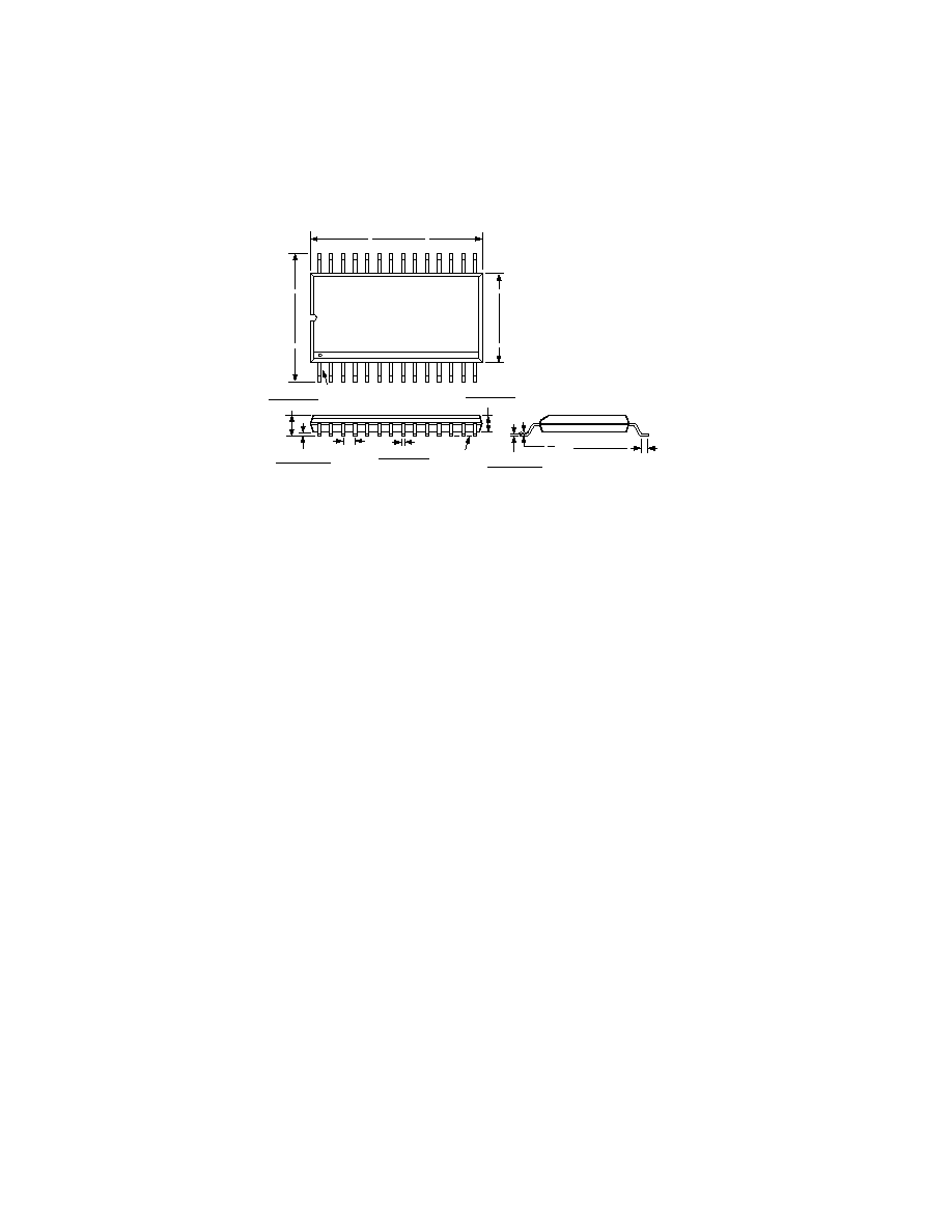
OUTLINE DIMENSIONS
Dimensions shown in inches and (mm).
28-Lead SSOP
(RS-28)
0.009 (0.229)
0.005 (0.127)
0.03 (0.762)
0.022 (0.558)
8∞
0∞
0.008 (0.203)
0.002 (0.050)
0.07 (1.79)
0.066 (1.67)
0.078 (1.98)
0.068 (1.73)
0.015 (0.38)
0.010 (0.25)
SEATING
PLANE
0.0256
(0.65)
BSC
0.311 (7.9)
0.301 (7.64)
0.212 (5.38)
0.205 (5.21)
28
15
14
1
0.407 (10.34)
0.397 (10.08)
PIN 1