 | ÐлекÑÑоннÑй компоненÑ: AD5555CRU | СкаÑаÑÑ:  PDF PDF  ZIP ZIP |
Äîêóìåíòàöèÿ è îïèñàíèÿ www.docs.chipfind.ru
Dual, Current-Output,
Serial-Input, 16-/14-Bit DAC
AD5545/AD5555
Rev. 0
Information furnished by Analog Devices is believed to be accurate and reliable.
However, no responsibility is assumed by Analog Devices for its use, nor for any
infringements of patents or other rights of third parties that may result from its use.
Specifications subject to change without notice. No license is granted by implication
or otherwise under any patent or patent rights of Analog Devices. Trademarks and
registered trademarks are the property of their respective companies.
One Technology Way, P.O. Box 9106, Norwood, MA 02062-9106, U.S.A.
Tel: 781.329.4700
www.analog.com
Fax: 781.326.8703
© 2003 Analog Devices, Inc. All rights reserved.
FEATURES
16-bit resolution AD5545
14-bit resolution AD5555
±1 LSB DNL monotonic
±2 LSB INL AD5545
2 mA full-scale current ±20%, with V
REF
= 10 V
0.5 µs settling time
2Q multiplying reference-input 4 MHz BW
Zero or midscale power-up preset
Zero or midscale dynamic reset
3-wire interface
Compact TSSOP-16 package
APPLICATIONS
Automatic test equipment
Instrumentation
Digitally controlled calibration
Industrial control PLCs
Programmable attentuator
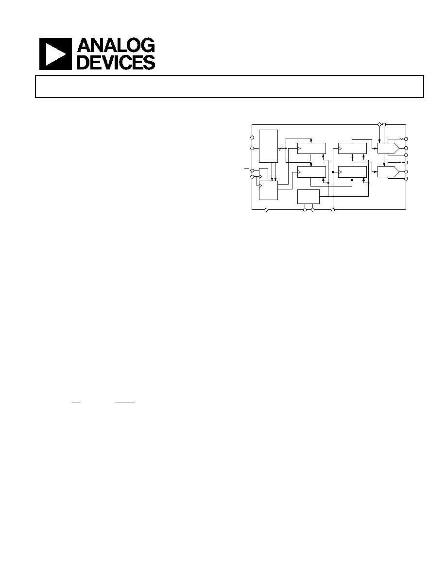
PRODUCT OVERVIEW
The AD5545/AD5555 are 16-bit/14-bit, current-output, digital-
to-analog converters designed to operate from a single 5 V
supply with bipolar output up to ±15 V capability.
An external reference is needed to establish the full-scale out-
put-current. An internal feedback resistor (R
FB
) enhances the
resistance and temperature tracking when combined with an
external op amp to complete the I-to-V conversion.
A serial data interface offers high speed, 3-wire microcontroller
compatible inputs using serial data in (SDI), clock (CLK), and
chip select (CS). Additional LDAC function allows simultane-
ous update operation. The internal reset logic allows power-on
preset and dynamic reset at either zero or midscale, depending
on the state of the MSB pin.
The AD5545/AD5555 are packaged in the compact TSSOP-16
package and can be operated from 40°C to +85°C.
FUNCTIONAL BLOCK DIAGRAM
AD5545/
AD5555
V
DD
R
FB
A
V
REF
B
V
REF
A
I
OUT
A
A
GND
A
SDI
CS
CLK
DGND
MSB
RS
LDAC
DAC A
DAC A
B
D0..DX
EN
R
R
R
R
16 OR 14
ADDR
DECODE
INPUT
REGISTER
POWER-
ON
RESET
INPUT
REGISTER
DAC A
REGISTER
DAC B
REGISTER
R
FB
B
I
OUT
B
A
GND
B
DAC B
02918-0-001
Figure 1.

AD5545/AD5555
TABLE OF CONTENTS
AD5545/AD5555--Electrical Characteristics .............................. 3
Absolute Maximum Ratings............................................................ 5
Pin Configuration And Functional Descriptions......................... 6
Typical Performance Characteristics ............................................. 9
Circuit Operation ........................................................................... 11
D/A Converter Section .............................................................. 11
Serial Data Interface................................................................... 11
Power-Up Sequence ................................................................... 12
Layout and Power Supply Bypassing ....................................... 12
Grounding ................................................................................... 12
Applications..................................................................................... 13
Stability ........................................................................................ 13
Positive Voltage Output ............................................................. 13
Bipolar Output............................................................................ 13
Programmable Current Source ................................................ 13
DAC with Programmable Input Reference Range................ 14
Outline Dimensions ....................................................................... 16
ESD Caution................................................................................ 16
Ordering Guide .......................................................................... 16
REVISION HISTORY
Revision 0: Initial Version
Rev. 0 | Page 2 of 16

AD5545/AD5555
Rev. 0 | Page 3 of 16
AD5545/AD5555--ELECTRICAL CHARACTERISTICS
Table 1. V
DD
= 5 V ± 10%, I
OUT
= Virtual GND, GND = 0 V, V
REF
= 10 V, T
A
= Full Operating Tempearture Range,
unless otherwise noted.
Parameter
Symbol
Conditions
5 V ± 10%
Units
STATIC PERFORMANCE
1
Resolution
N
AD5545, 1 LSB = V
REF
/2
16
= 153 µV when V
REF
= 10 V
16
Bits
Resolution
N
AD5555, 1 LSB = V
REF
/2
14
= 610 µV when V
REF
= 10 V
14
Bits
Relative Accuracy
INL
AD5545
±2
LSB max
Relative Accuracy
INL
AD5555
±1
LSB max
Differential Nonlinearity
DNL
Monotonic
±1
LSB max
Output Leakage Current
I
OUT
Data = 0x0000, T
A
= 25°C
10
nA max
Output Leakage Current
I
OUT
Data = 0x0000, T
A
= T
A
Max
20
nA max
Full-Scale Gain Error
G
FSE
Data = Full Scale
±1/±4
mV typ/max
Full-Scale Temperature Coefficient
2
TCV
FS
1
ppm/°C
typ
REFERENCE INPUT
V
REF
Range
V
REF
12/+12
V min/V max
Input Resistance
R
REF
5
k
typ
3
Input Capacitance
2
C
REF
5
pF
typ
ANALOG OUTPUT
Output Current
I
OUT
Data = Full Scale
2
mA typ
Output Capacitance
2
C
OUT
Code Dependent
200
pF typ
LOGIC INPUTS AND OUTPUT
Logic Input Low Voltage
V
IL
0.8 V
max
Logic Input High Voltage
V
IH
2.4 V
min
Input Leakage Current
I
IL
10 µA
max
Input Capacitance
2
C
IL
10 pF
max
INTERFACE TIMING
2, 4
Clock Input Frequency
f
CLK
50 MHz
Clock Width High
t
CH
10 ns
min
Clock Width Low
t
CL
10 ns
min
CS to Clock Setup
t
CSS
0
ns
min
Clock to CS Hold
t
CSH
10 ns
min
Data Setup
t
DS
5 ns
min
Data Hold
t
DH
10 ns
min
LDAC Setup
t
LDS
5
ns
min
Hold
t
LDH
10 ns
min
LDAC Width
t
LDAC
10
ns
min
SUPPLY CHARACTERISTICS
Power Supply Range
V
DD
Range
4.5/5.5
V min/V max
Positive Supply Current
I
DD
Logic Inputs = 0 V
10
µA max
Power Dissipation
P
DISS
Logic Inputs = 0 V
0.055
mW max
Power Supply Sensitivity
PSS
V
DD
= ±5%
0.006
%/% max
1
All static performance tests (except I
OUT
) are performed in a closed-loop system using an external precision OP1177 I-to-V converter amplifier. The AD5545 R
FB
terminal
is tied to the amplifier output. Typical values represent average readings measured at 25°C.
2
These parameters are guaranteed by design and not subject to production testing.
3
All ac characteristic tests are performed in a closed-loop system using an O42 I-to-V converter amplifier.
4
All input control signals are specified with t
R
= t
F
= 2.5 ns (10% to 90% of 3 V) and timed from a voltage level of 1.5 V.

AD5545/AD5555
Parameter
Symbol
Conditions
5 V ± 10%
Units
AC CHARACTERISTICS
Output Voltage Setting Time
t
S
To ±0.1% Full Scale, Data = Zero Scale to
Full Scale to Zero Scale
0.5 µs
typ
Reference Multiplying BW
BW
V
REF
= 5 V p-p, Data = Full Scale
4
MHz typ
DAC Glitch Impulse
Q
V
REF
= 0 V, Data = Zero Scale to Midscale to Zero
Scale
7 nV-s
typ
Feedthrough Error
V
OUT
/V
REF
Data = Zero Scale, V
REF
= 100 mV rms,
f = 1 kHz, Same Channel
65 dB
Digital Feedthrough
Q
CS = Logic High and f
CLK
= 1 MHz
7 nV-s
typ
Total Harmonic Distortion
THD
V
REF
= 5 V p-p, Data = Full Scale, f = 1 kHz to 10 kHz
85
dB typ
Analog Crosstalk
C
TA
V
REFB
= 0 V, Measure V
OUTB
with V
REFA
= 5 V p-p Sine
Wave, Data = Full Scale, f = 1 kHz to 10 kHz
95 dB
typ
Output Spot Noise Voltage
e
N
f = 1 kHz, BW = 1 Hz
12
nV/Hz
Rev. 0 | Page 4 of 16

AD5545/AD5555
ABSOLUTE MAXIMUM RATINGS
Table 2. AD5545/AD5555 Absolute Maximum Ratings
Parameter Rating
V
DD
to GND
0.3 V, +8 V
V
REF
to GND
18 V, +18 V
Logic Inputs to GND
0.3 V, +8 V
V(I
OUT
) to GND
0.3 V, V
DD
+ 0.3 V
Input Current to Any Pin except Supplies
±50 mA
Package Power Dissipation
(T
J
max T
A
)/ JA
Thermal Resistance
JA
16-Lead TSSOP
150°C/W
Maximum Junction Temperature (T
J
max)
150°C
Operating Temperature Range
40°C to +85°C
Storage Temperature Range
65°C to +150°C
Lead Temperature
RU-16 (Vapor Phase, 60 sec)
215°C
RU-16 (Infrared, 15 sec)
220°C
Stresses above those listed under Absolute Maximum Ratings may cause permanent damage to the device. This is a stress rating only and
functional operation of the device at these or any other conditions above those indicated in the operational section of this specification is
not implied. Exposure to absolute maximum rating conditions for extended periods may affect device reliability.
Rev. 0 | Page 5 of 16
AD5545/AD5555
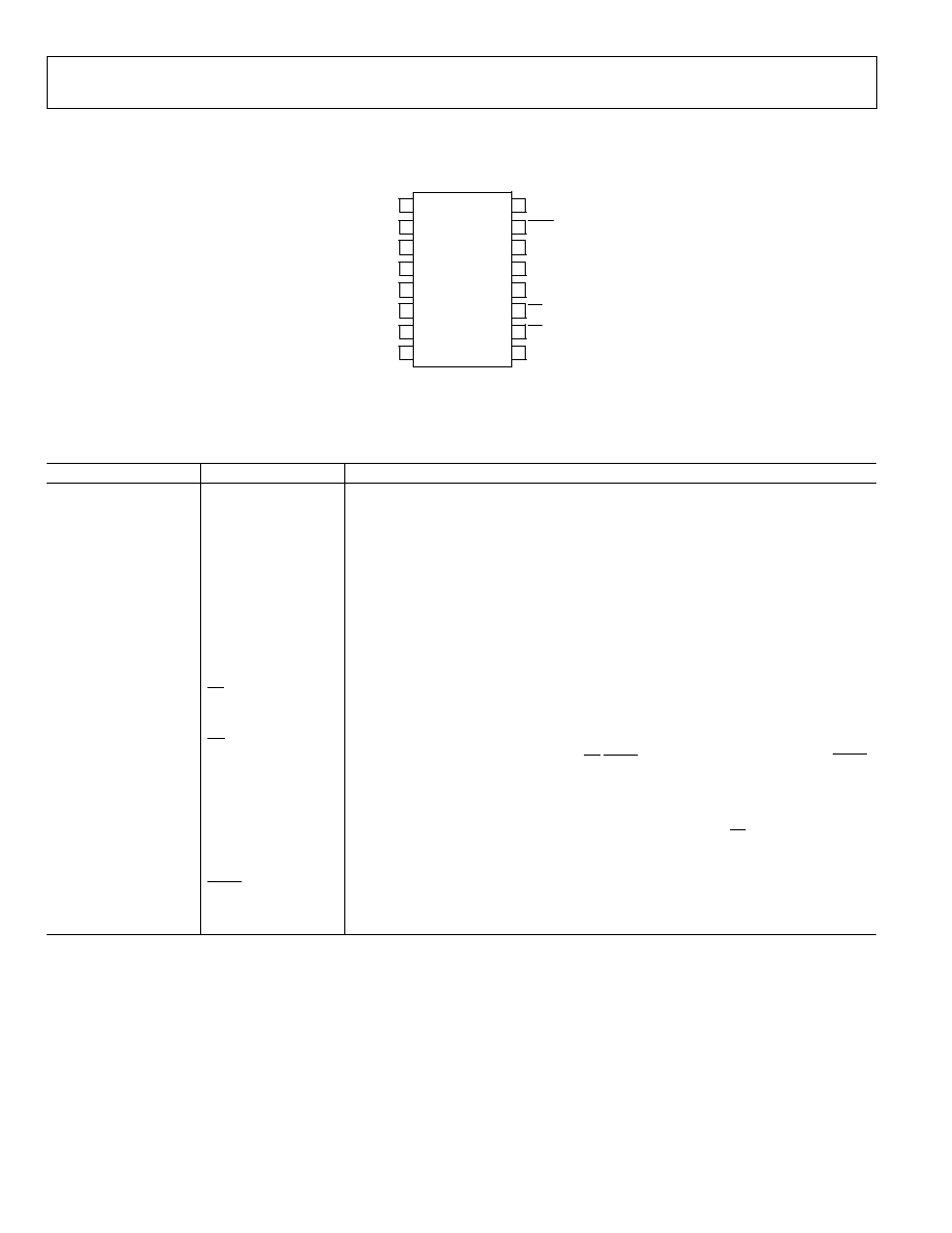
PIN CONFIGURATION AND FUNCTIONAL DESCRIPTIONS
AD5545/
AD5555
TOP VIEW
(Not to Scale)
8
7
6
5
1
4
3
2
9
10
11
12
16
13
14
15
CS
DGND
CLK
V
DD
MSB
LDAC
RS
SDI
V
REF
B
R
FB
B
A
GND
B
I
OUT
B
R
FB
A
A
GND
A
I
OUT
A
V
REF
A
02918-0-002
Figure 2. 16-Lead TSSOP
Table 3. Pin Function Descriptions--16-Lead TSSOP
Pin No.
Mnemonic
Function
1 R
FB
A
Establish voltage output for DAC A by connecting to external amplifier output.
2 V
REF
A
DAC A Reference Voltage Input Terminal. Establishes DAC A full-scale output voltage.
Pin can be tied to V
DD
pin.
3 I
OUT
A
DAC A Current Output.
4 A
GND
A
DAC A Analog Ground.
5 A
GND
B
DAC B Analog Ground.
6 I
OUT
B
DAC B Current Output.
7 V
REF
B
DAC B Reference Voltage Input Terminal. Establishes DAC B full-scale output voltage.
Pin can be tied to V
DD
pin.
8 R
FB
B
Establish voltage output for DAC B by connecting to external amplifier output.
9
SDI
Serial Data Input. Input data loads directly into the shift register.
10
RS
RESET Pin, Active Low Input. Input registers and DAC registers are set to all 0s or
midscale. Register Data = 0x0000 when MSB = 0. Register Data = 0x8000 for AD5545 and
0x2000 for AD5555 when MSB = 1.
11
CS
Chip Select, Active Low Input. Disables shift register loading when high. Transfers serial
register data to the input register when CS/LDAC returns high. This does not affect LDAC
operation.
12
DGND
Digital Ground Pin.
13 V
DD
Positive Power Supply Input. Specified range of operation 5 V ± 10% or 3 V ± 10%.
14 MSB
MSB bit sets output to either 0 or midscale during a RESET pulse (RS) or at system power-
on. Output equals zero scale when MSB = 0 and midscale when MSB = 1. MSB pin can
also be tied permanently to ground or V
DD
.
15
LDAC
Load DAC Register Strobe, Level Sensitive Active Low. Transfers all input register data to
DAC registers. Asynchronous active low input. See Table 4 and Table 5 for operation.
16
CLK
Clock Input. Positive edge clocks data into shift register.
Rev. 0 | Page 6 of 16
AD5545/AD5555
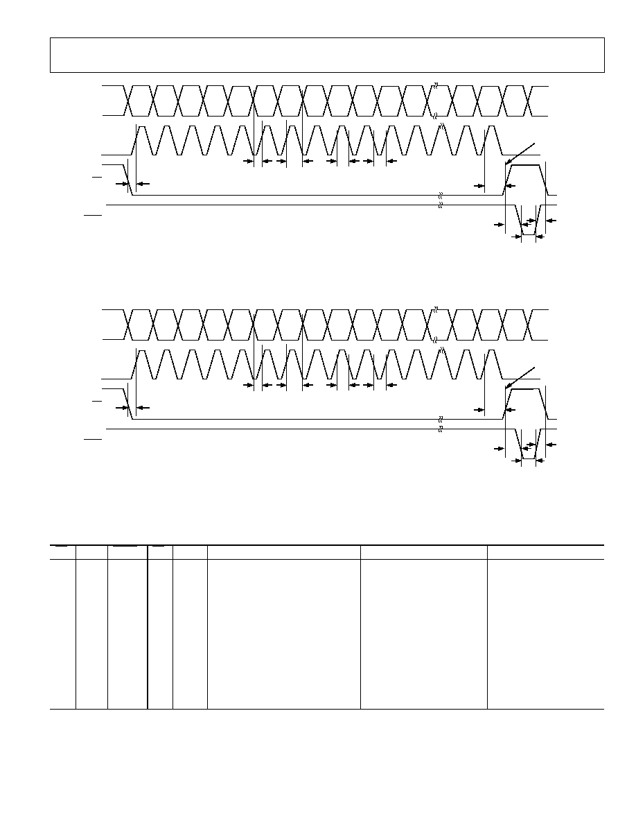
Rev. 0 | Page 7 of 16
02918- 0-003
A1
SDI
CLK
CS
t
CSS
t
DS
t
DH
t
CH
t
CL
t
LDAC
t
CSH
t
LDS
t
LDH
LDAC
A0
INPUT REG LD
D1
D0
D15
D14
D13
D12
D11
D10
Figure 3. AD5545 18-Bit Data Word Timing Diagram
02918- 0-004
A1
SDI
CLK
CS
t
CSS
t
DS
t
DH
t
CH
t
CL
t
LDAC
t
CSH
t
LDS
t
LDH
LDAC
A0
INPUT REG LD
D1
D0
D13
D12
D11
D10
D09
D08
Figure 4. AD5555 16-Bit Data Word Timing Diagram
Table 4. AD5545 Control Logic Truth Table
CS CLK LDAC
RS
MSB
Serial Shift Register Function
Input Register Function
DAC Register
H X H
H X
No
Effect
Latched
Latched
L L H
H X No
Effect
Latched
Latched
L
+
H H
X
Shift Register Data
Advanced One Bit
Latched Latched
L H H
H X No
Effect
Latched
Latched
+
L H H
X No
Effect
Selected DAC Updated
with Current SR Current
Latched
H X L
H X
No
Effect
Latched
Transparent
H X H
H X
No
Effect
Latched
Latched
H X
+
H X
No
Effect
Latched
Latched
H
X
H
L
0
No Effect
Latched Data = 0x0000
Latched Data = 0x0000
H
X
H
L
H
No Effect
Latched Data = 0x8000
Latched Data = 0x8000
NOTES
1. SR = Shift Register, + = Positive Logic Transition, and X = Don't Care.
2. At power-on, both the input register and the DAC register are loaded with all 0s.
AD5545/AD5555
Table 5. AD5555 Control Logic Truth Table
CS CLK LDAC
RS
MSB
Serial Shift Register Function
Input Register Function
DAC Register
H X H
H X
No
Effect
Latched
Latched
L L H
H X No
Effect
Latched
Latched
L
+
H H
X
Shift Register Data
Advanced One Bit
Latched Latched
L H H
H X No
Effect
Latched
Latched
+
L H H
X No
Effect
Selected DAC Updated
with Current SR Current
Latched
H X L
H X
No
Effect
Latched
Transparent
H X H
H X
No
Effect
Latched
Latched
H X
+
H X
No
Effect
Latched
Latched
H
X
H
L
0
No Effect
Latched Data = 0x0000
Latched Data = 0x0000
H
X
H
L
H
No Effect
Latched Data = 0x2000
Latched Data = 0x2000
NOTES
1. SR = Shift Register, + = Positive Logic Transition, and X = Don't Care.
2. At power-on, both the input register and the DAC register are loaded with all 0s.
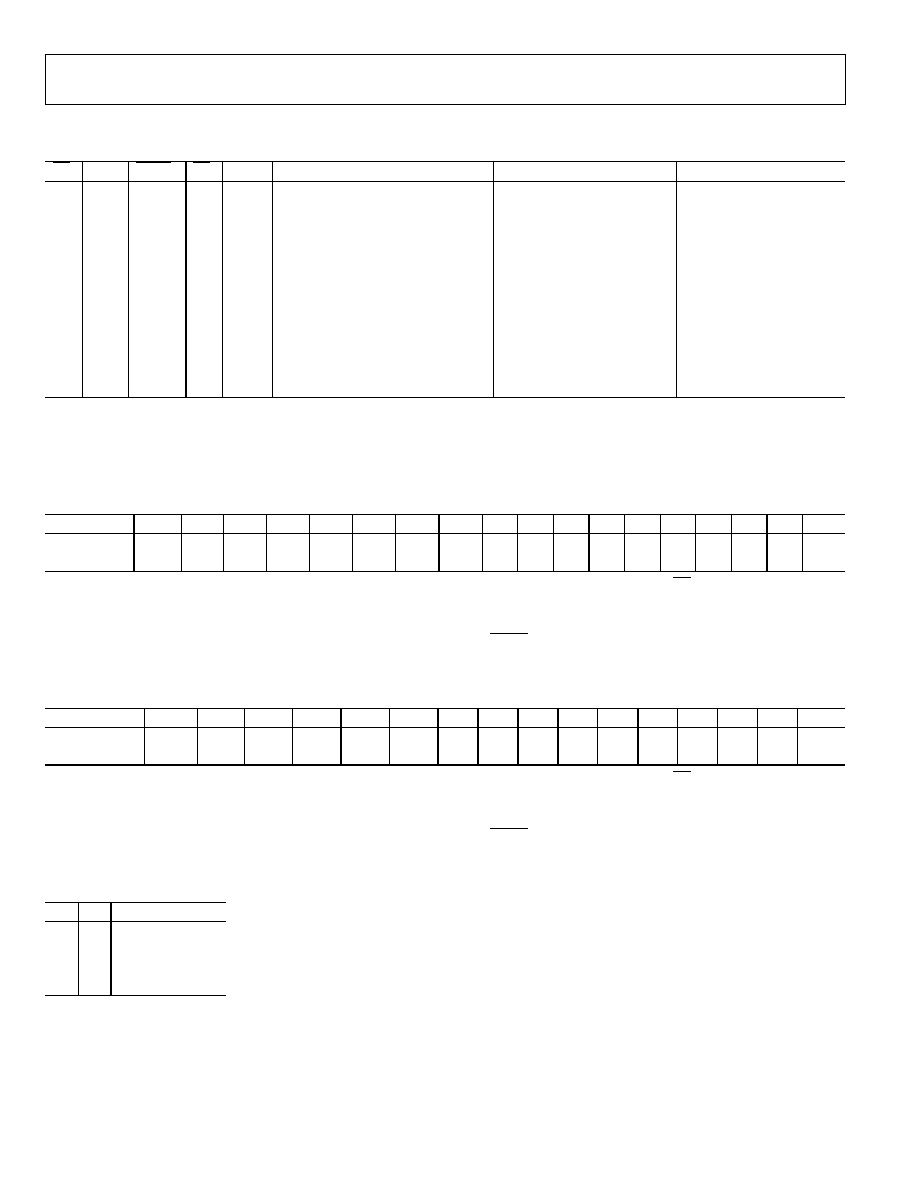
Table 6. AD5545 Serial Input Register Data Format, Data Is Loaded in the MSB-First Format
MSB
LSB
Bit
Position B17 B16 B15 B14 B13 B12 B11 B10 B9 B8 B7 B6 B5 B4 B3 B2 B1 B0
Data
Word A1
A0 D15 D14 D13 D12 D11 D10 D9 D8 D7 D6 D5 D4 D3 D2 D1 D0
Note that only the last 18 bits of data clocked into the serial register (Address + Data) are inspected when the CS line's positive edge
returns to logic high. At this point, an internally generated load strobe transfers the serial register data contents (Bits D15D0) to the
decoded DAC input register address determined by Bits A1 and A0. Any extra bits clocked into the AD5545 shift register are ignored; only
the last 18 bits clocked in are used. If double-buffered data is not needed, the LDAC pin can be tied logic low to disable the DAC registers.
Table 7. AD5555 Serial Input Register Data Format, Data Is Loaded in the MSB-First Format
MSB
LSB
Bit
Position B15 B14 B13 B12 B11 B10 B9 B8 B7 B6 B5 B4 B3 B2 B1 B0
Data
Word
A1
A0 D13 D12 D11 D10 D9 D8 D7 D6 D5 D4 D3 D2 D1 D0
Note that only the last 16 bits of data clocked into the serial register (Address + Data) are inspected when the CS line's positive edge
returns to logic high. At this point, an internally generated load strobe transfers the serial register data contents (Bits D13D0) to the
decoded DAC input register address determined by Bits A1 and A0. Any extra bits clocked into the AD5555 shift register are ignored; only
the last 16 bits clocked in are used. If double-buffered data is not needed, the LDAC pin can be tied logic low to disable the DAC registers.
Table 8. Address Decode
A1 A0 DAC
Decoded
0 0 None
0 1 DAC
A
1 0 DAC
B
1
1
DAC A and DAC B
Rev. 0 | Page 8 of 16
AD5545/AD5555
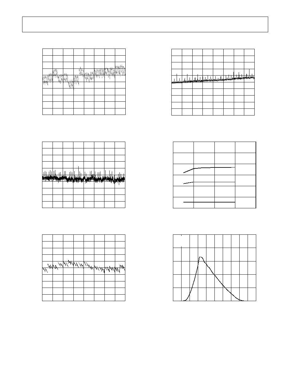
TYPICAL PERFORMANCE CHARACTERISTICS
1.0
0.8
0.6
0
8192
16384 24576 32768 40960 49152 57344 65536
0.4
0.2
0
0.2
0.4
0.6
0.8
1.0
INL
(
LSB)
CODE (Decimal)
02918-0-009
Figure 5. AD5545 Integral Nonlinearity Error
1.0
0.8
0.6
0
8192
16384 24576 32768 40960 49152 57344 65536
0.4
0.2
0
0.2
0.4
0.6
0.8
1.0
DNL (LS
B
)
CODE (Decimal)
02918- 0-010
Figure 6. AD5545 Differential Nonlinearity Error
1.0
0.8
0.6
0
2048
4096
6144
8192
10240 12288 14336 16384
0.4
0.2
0
0.2
0.4
0.6
0.8
1.0
INL (
L
SB)
CODE (Decimal)
02918-0-011
Figure 7. AD5555 Integral Nonlinearity Error
1.0
0.8
0.6
0
0248
4096
6144
8192
10240 12288 14336 16384
0.4
0.2
0
0.2
0.4
0.6
0.8
1.0
DNL (LS
B
)
CODE (Decimal)
02918-0- 012
Figure 8. AD5555 Differential Nonlinearity Error
1.5
1.0
2
4
GE
DNL
INL
6
8
0.5
0
0.5
1.0
1.5
LINE
ARITY
E
RROR (LS
B
)
SUPPLY VOLTAGE V
DD
(V)
V
REF
= 2.5V
T
A
= 25°C
02918- 0-013
10
Figure 9. Linearity Errors vs. V
DD
5
4
0
0.5
1.0
1.5
2.0
3.0
3.5
2.5
4.0
4.5
5.0
3
2
1
0
S
U
P
P
L
Y
CURRE
NT I
DD
(LS
B
)
LOGIC INPUT VOLTAGE V
IH
(V)
V
DD
= 5V
T
A
= 25°C
02918-0-014
Figure 10. Supply Current vs. Logic Input Voltage
Rev. 0 | Page 9 of 16
AD5545/AD5555
Rev. 0 | Page 10 of 16
3.0
2.5
10k
100k
1M
10M
100M
2.0
1.5
1.0
0.5
0
S
U
P
P
L
Y
CURRE
NT (mA)
CLOCK FREQUENCY (Hz)
0x5555
0x8000
0xFFFF
0x0000
02918-0- 015
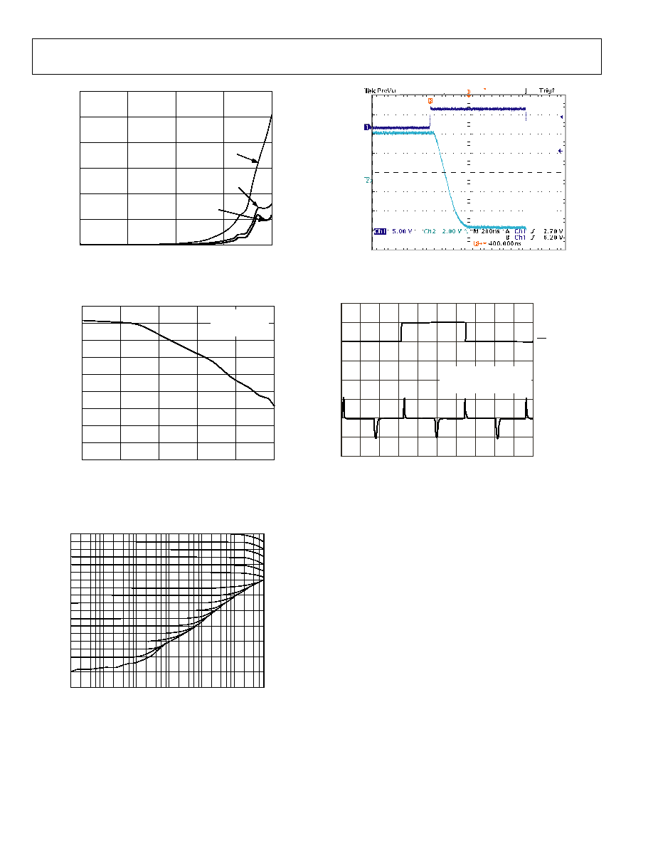
Figure 11. Supply Current vs. Clock Frequency
90
70
10
100
1k
10k
100k
1M
50
40
60
80
30
10
20
0
PSSR
(
-
d
B
)
FREQUENCY (Hz)
V
DD
= 5V ± 10%
V
REF
= 10V
02918- 0-016
Figure 12. Power Supply Rejection Ration vs. Frequency
0xFFFF
0x8000
0x4000
12dB
24dB
36dB
48dB
60dB
72dB
84dB
96dB
108dB
0x2000
0x1000
0x0800
0x0400
0x0200
0x0100
0x0080
0x0040
0x0020
0x0010
0x0008
0x0004
0x0002
0x0001
0x0000
10
100
1k
100k
10k
1M
10M
START 10.000Hz
STOP 50 000 000.000Hz
REF LEVEL
0.000dB
/DIV
12.000dB
MARKER 4 41 677.200Hz
MAG (A/R) 2.939db
02918- 0-017
Figure 13. Reference Multiplying Bandwidth
02918-0-018
V
OUT
CS
Figure 14. Settling Time
0
0.5
1.0
1.5
2.0
2.5
3.0
3.5
4.0
4.5
5.0
V
DD
= 5V
V
REF
= 10V
CODES 0x8000
0x7FFF
TIME (
µs)
V
OUT
(50mV/DIV)
CS (5V/DIV)
02918-0-019
Figure 15. Midscale Transition and Digital Feedthrough
AD5545/AD5555
Rev. 0 | Page 11 of 16
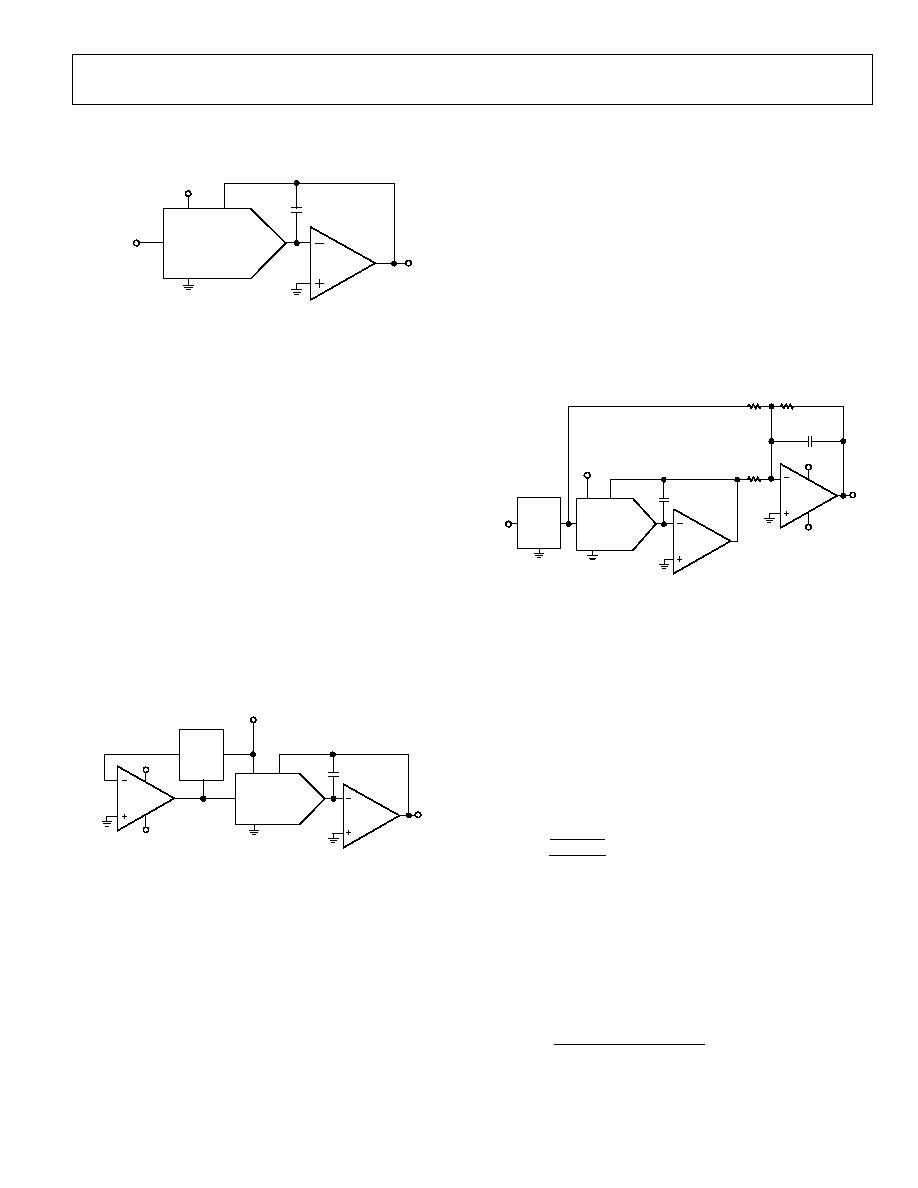
CIRCUIT OPERATION
The AD5545/AD5555 contain a 16-/14-bit, current-output,
digital-to-analog converter, a serial-input register, and a DAC
register. Both parts require a minimum of a 3-wire serial data
interface with additional LDAC for dual channel simultaneous
update.
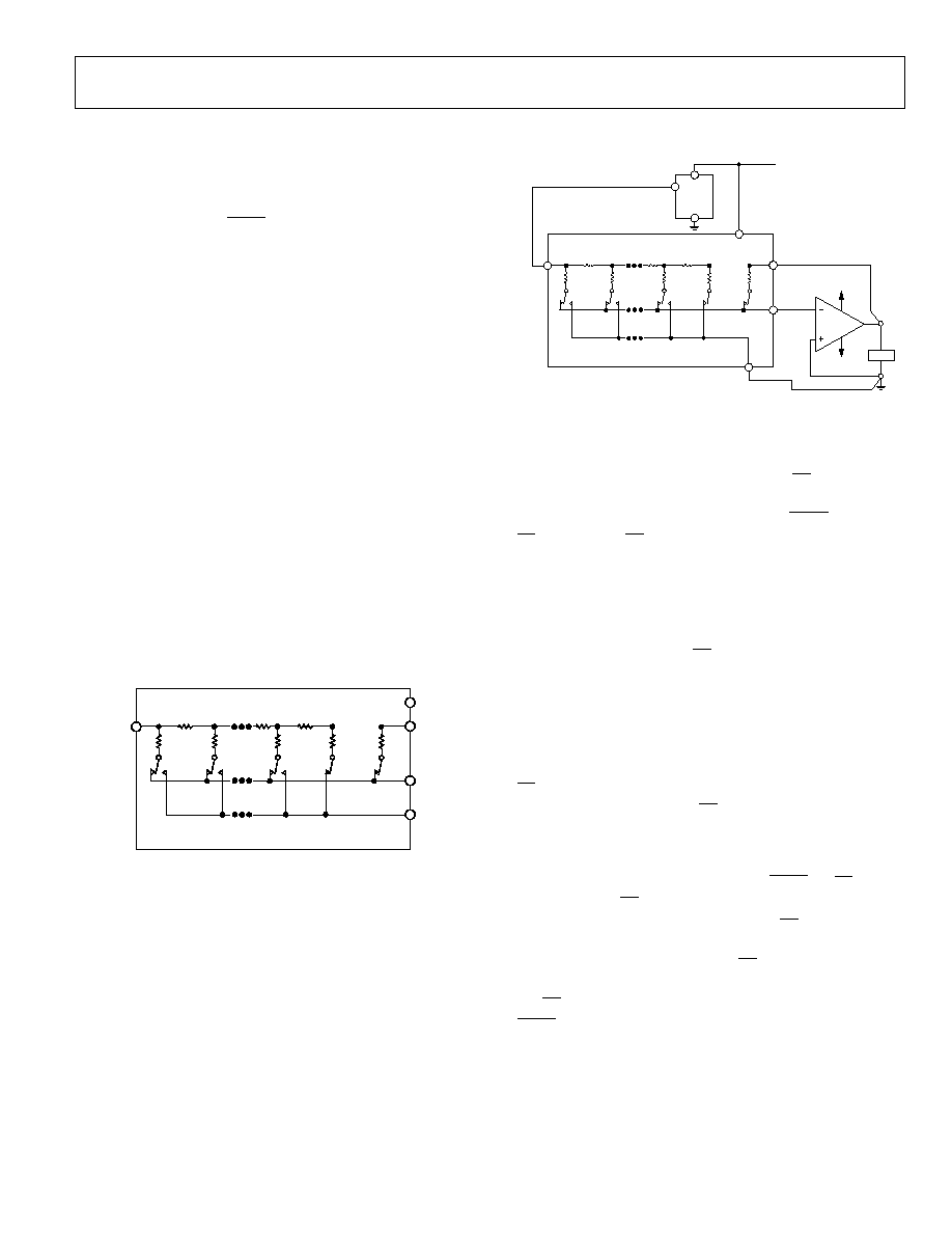
D/A CONVERTER SECTION
The DAC architecture uses a current-steering R-2R ladder
design. Figure 16 shows the typical equivalent DAC. The DAC
contains a matching feedback resistor for use with an external
I-to-V converter amplifier. The R
FB
pin is connected to the
output of the external amplifier. The I
OUT
terminal is connected
to the inverting input of the external amplifier. These DACs are
designed to operate with both negative or positive reference
voltages. The V
DD
power pin is used only by the logic to drive
the DAC switches ON and OFF. Note that a matching switch is
used in series with the internal 5 k feedback resistor. If users
attempt to measure the R
FB
value, power must be applied to V
DD
to achieve continuity. The V
REF
input voltage and the digital data
(D) loaded into the corresponding DAC register, according to
Equation 1 and Equation 2, determine the DAC output voltage.
536
,
65
/
D
V
V
REF
OUT
×
=
(1)
384
,
16
/
D
V
V
REF
OUT
×
=
(2)
Note that the output full-scale polarity is the opposite of the
V
REF
polarity for dc reference voltages.
V
REF
DIGITAL INTERFACE CONNECTIONS OMITTED FOR CLARITY:
SWITCHES S1 AND S2 ARE CLOSED, V
DD
MUST BE POWERED
R
2R
2R
2R
R
5k
S2
S1
R
R
V
DD
R
FB
I
OUT
GND
02918-0-005
Figure 16. Equivalent R-2R DAC Circuit
These DACs are also designed to accommodate ac reference
input signals. The AD5545/AD5555 will accommodate input
reference voltages in the range of 12 V to +12 V. The reference
voltage inputs exhibit a constant nominal input-resistance value
of 5 k, ±30%. The DAC output (I
OUT
) is code dependent,
producing various output resistances and capacitances. When
choosing an external amplifier, the user should take into
account the variation in impedance generated by the
AD5545/AD5555 on the amplifiers inverting input node. The
feedback resistance in parallel with the DAC ladder resistance
dominates output voltage noise.
V
REF
A
DIGITAL INTERFACE CONNECTIONS OMITTED FOR CLARITY:
SWITCHES S1 AND S2 ARE CLOSED, V
DD
MUST BE POWERED
R
2R
2R
2R
R
5k
S2
S1
+3V
3V
R
R
V
OUT
V
IN
V
DD
5V
2.500V
R
FB
A
I
OUT
A
A
GND
A
GND
02918-0-006
AD5545/AD5555
ADR03
AD8628
LOAD
V
OUT
V
EE
V
CC
Figure 17. Recommended System Connections
SERIAL DATA INTERFACE
The AD5545/AD5555 use a minimum 3-wire (CS, SDI, CLK)
serial data interface for single channel update operation. With
Table 4 as an example (AD5545), users can tie LDAC low and
RS high, then pull CS low for an 18-bit duration. New serial data
is then clocked into the serial-input register in an 18-bit data-
word format with the MSB bit loaded first. Table 5 defines the
truth table for the AD5555. Data is placed on the SDI pin and
clocked into the register on the positive clock edge of CLK. For
the AD5545, only the last 18-bits clocked into the serial register
will be interrogated when the CS pin is strobed high, transfer-
ring the serial register data to the DAC register and updating
the output. If the applied microcontroller outputs serial data in
different lengths than the AD5545, such as 8-bit bytes, three
right justified data bytes can be written to the AD5545. The
AD5545 will ignore the six MSB and recognize the 18 LSB as
valid data. After loading the serial register, the rising edge of
CS transfers the serial register data to the DAC register and
updates the output; during the CS strobe, the CLK should not
be toggled.
If users want to program each channel separately but update
them simultaneously, they need to program LDAC and RS high
initially, then pull CS low for an 18-bit duration and program
DAC A with the proper address and data bits. CS is then pulled
high to latch data to the DAC A register. At this time, the output is
not updated. To load DAC B data, pull CS low for an 18-bit dura-
tion and program DAC B with the proper address and data, then
pull CS high to latch data to the DAC B register. Finally, pull
LDAC low and then high to update both the DAC A and DAC B
outputs simultaneously.
AD5545/AD5555
Rev. 0 | Page 12 of 16
Table 8 shows that each DAC A and DAC B can be individually
loaded with a new data value. In addition, a common new data
value can be loaded into both DACs simultaneously by setting Bit
A1 = A0 = high. This command enables the parallel combination
of both DACs, with I
OUT
A and I
OUT
B tied together, to act as one
DAC with significant improved noise performance.
LAYOUT AND POWER SUPPLY BYPASSING
It is a good practice to employ compact, minimum lead length
layout design. The input leads should be as direct as possible
with a minimum conductor length. Ground paths should have
low resistance and low inductance.
Similarly, it is also good practice to bypass the power supplies
with quality capacitors for optimum stability. Supply leads to the
device should be bypassed with 0.01 µF to 0.1 µF disc or chip
ceramic capacitors. Low ESR 1 µF to 10 µF tantalum or electro-
lytic capacitors should also be applied at V
DD
to minimize any
transient disturbance and to filter any low frequency ripple
(see Figure 19). Users should not apply switching regulators for
V
DD
due to the power supply rejection ratio degradation over
frequency.
ESD Protection Circuits
All logic input pins contain back-biased ESD protection Zeners
connected to digital ground (DGND) and V
DD
as shown in
Figure 18.
V
DD
02918- 0-007
5k
DGND
DIGITAL
INPUTS
AD5545/
AD5555
V
DD
V
DD
A
GND
X
DGND
02918-0-008
C1
+
C2
10
µF
0.1
µF
Figure 18. Equivalent ESD Protection Circuits
POWER-UP SEQUENCE
It is recommended to power-up V
DD
and ground prior to any
reference voltages. The ideal power-up sequence is A
GND
X,
DGND, V
DD
, V
REF
X, and digital inputs. A noncompliance power-
up sequence can elevate reference current, but the device will
resume normal operation once V
DD
is powered.
Figure 19. Power Supply Bypassing and Grounding Connection
GROUNDING
The DGND and A
GND
X pins of the AD5545/AD5555 refer to the
digital and analog ground references. To minimize the digital
ground bounce, the DGND terminal should be joined remotely
at a single point to the analog ground plane (see Figure 19).
AD5545/AD5555
Rev. 0 | Page 13 of 16
APPLICATIONS
STABILITY
AD5545/AD5555
AD8628
V
REF
V
REF
I
OUT
V
O
V
DD
V
DD
R
FB
U1
U2
C1
GND
02918-0-020
Figure 20. Operational Compensation Capacitor for Gain Peaking Prevention
In the I-to-V configuration, the I
OUT
of the DAC and the invert-
ing node of the op amp must be connected as close as possible,
and proper PCB layout techniques must be employed. Since
every code change corresponds to a step function, gain peaking
may occur if the op amp has limited GBP, and if there is exces-
sive parasitic capacitance at the inverting node.
An optional compensation capacitor, C1, can be added for sta-
bility as shown in Figure 20. C1 should be found empirically, but
20 pF is generally more than adequate for the compensation.
POSITIVE VOLTAGE OUTPUT
To achieve the positive voltage output, an applied negative
reference to the input of the DAC is preferred over the output
inversion through an inverting amplifier because of the resis-
tors' tolerance errors. To generate a negative reference, the
reference can be level shifted by an op amp such that the V
OUT
and GND pins of the reference become the virtual ground and
2.5 V, respectively (see Figure 21).
AD5545/AD5555
1/2
AD8628
1/2
AD8620
ADR03
V
REF
I
OUT
V
OUT
V
IN
V
DD
GND
GND
02918-0-021
V
O
0 < V
O
< +2.5
R
FB
U2
U1
+5V
V+
5V
V
+5V
2.5V
U3
C1
U4
Figure 21. Positive Voltage Output Configuration
BIPOLAR OUTPUT
The AD5545/AD5555 is inherently a 2-quadrant multiplying
D/A converter. It can easily set up for unipolar output opera-
tion. The full-scale output polarity is the inverse of the reference
input voltage.
In some applications, it may be necessary to generate the full
4-quadrant multiplying capability or a bipolar output swing. This
is easily accomplished by using an additional external amplifier,
U4, configured as a summing amplifier (see Figure 22). In this
circuit, the second amplifier, U4, provides a gain of +2, which
increases the output span magnitude to 5 V. Biasing the external
amplifier with a 2.5 V offset from the reference voltage results in a
full 4-quadrant multiplying circuit. The transfer equation of this
circuit shows that both negative and positive output voltages are
created because the input data (D) is incremented from code zero
(V
OUT
= 2.5 V) to midscale (V
OUT
= 0 V) to full scale (V
OUT
=
+2.5 V).
(
)
(
5545
1
768
,
32
/
AD
V
D
V
REF
OUT
×
)
=
(3)
(
)
(
5555
1
384
,
16
/
AD
V
D
V
REF
OUT
×
)
=
(4)
For the AD5545, the external resistance tolerance becomes the
dominant error that users should be aware of.
AD5545/AD5555
1/2
AD8620
1/2
AD8620
ADR03
V
REF
I
OUT
V
OUT
V
IN
V
DD
GND
GND
02918-0-022
V
O
2.5 < V
O
< +2.5
R
FB
U2
U3
U1
+5V
+5V
V+
5V
5V
V
U4
C1
C2
R1
10k
±0.01% 10k±0.01%
5k
±0.01%
R2
R3
Figure 22. Four-Quadrant Multiplying Application Circuit
PROGRAMMABLE CURRENT SOURCE
Figure 23 shows a versatile V-to-I conversion circuit using
improved Howland Current Pump. In addition to the precision
current conversion it provides, this circuit enables a bidirec-
tional current flow and high voltage compliance. This circuit
can be used in a 4 mA to 20 mA current transmitter with up to
a 500 of load. In Figure 23, it shows that if the resistor net-
work is matched, the load current is
(
)
D
V
3
1
3
2
REF
×
×
+
=
R
R
R
R
I
L
(5)
R3, in theory, can be made small to achieve the current needed
within the U3 output current driving capability. This circuit is
versatile such that the AD8510 can deliver ±20 mA in both
directions, and the voltage compliance approaches 15 V, which
is mainly limited by the supply voltages of U3. However, users
must pay attention to the compensation. Without C1, it can be
shown that the output impedance becomes
(
)
(
)
(
)
3
2
1
3
2
1
2
1
3
1
R
R
R
R
R
R
R
R
R
R
Z
O
+
+
+
=
(6)
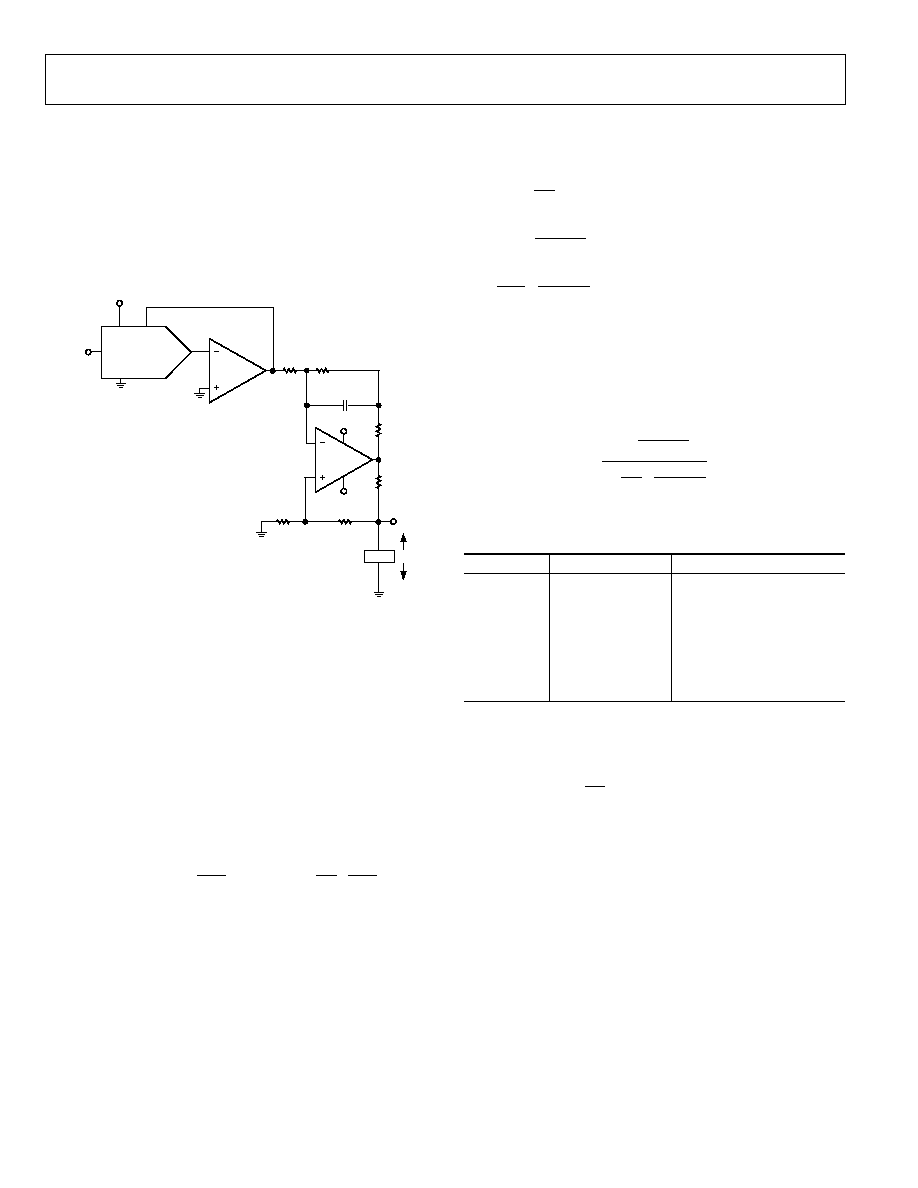
AD5545/AD5555
Rev. 0 | Page 14 of 16
If the resistors are perfectly matched, Z
O
is infinite, which is
desirable, and the resistors behave as an ideal current source.
On the other hand, if they are not matched, Z
O
can be either
positive or negative. The latter can cause oscillation. As a result,
C1 is needed to prevent the oscillation. For critical applications,
C1 could be found empirically but typically falls in the range of
a few pF.
R
WB
and R
WA
are digital potentiometer 128-step programmable
resistances and are given by
AB
C
WB
R
D
R
128
(8)
AB
C
WA
R
D
R
128
128 -
(9)
C
C
WA
WB
D
D
R
R
-
128
(10)
AD5545/AD5555
AD8628
AD8510
V
REF
V
REF
I
OUT
V
DD
V
DD
V
DD
C1
10pF
V
SS
LOAD
GND
02918-0- 023
V
L
I
L
R
FB
U2
U3
U1
V+
V
R3'
50
R1'
150k
R2'
15k
R1
150k
R2
15k
R3
50
where D
C
= Digital Potentiometer Digital Code in Decimal
(0 D
C
127).
By putting Equations 7 through 10 together, the following
results:
C
C
N
A
C
C
REF
REF
D
D
D
D
D
V
AB
V
-
×
-
-
+
×
=
128
2
1
128
1
(11)
Table 9 shows a few examples of V
REF
AB of the 14-bit AD5555.
Table 9. V
REF
AB
vs. D
B
and D
C
of the AD5555
D
C
D
A
V
REF
AB
0 X
V
REF
32 0
1.33
V
REF
32 8192
1.6
V
REF
64 0
2
V
REF
64 8192
4
V
REF
96 0
4
V
REF
96 8192
8
V
REF
Figure 23. Programmable Current Source with Bidirectional
Current Control and High Voltage Compliance Capabilities
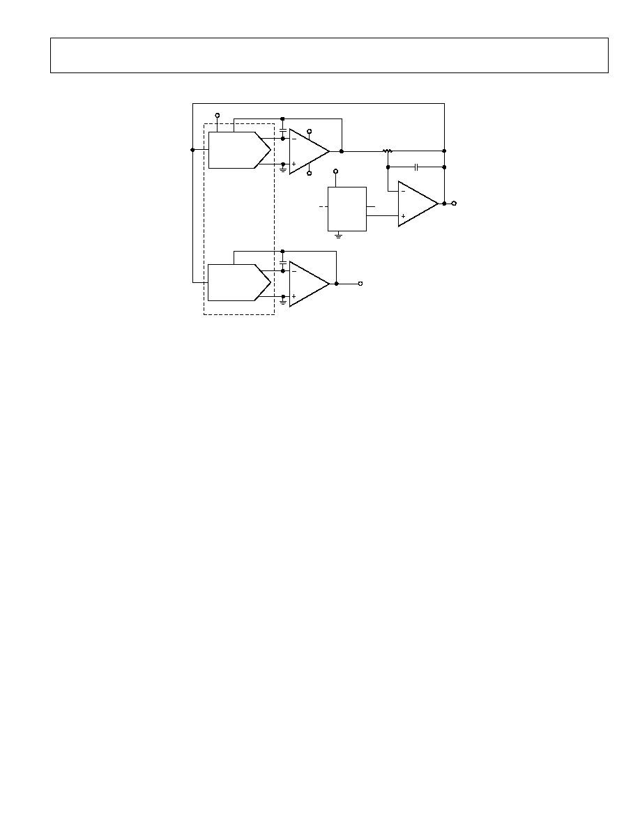
DAC WITH PROGRAMMABLE INPUT
REFERENCE RANGE
Since high voltage references can be costly, users may consider
using one of the DACs, a digital potentiometer, and a low
voltage reference to form a single-channel DAC with a
programmable input reference range. This approach optimizes
the programmable range as well as facilitates future system
upgrades with just software changes. Figure 24 shows this
implementation. V
REF
AB
is in the feedback network, therefore,
The output of DAC B is, therefore,
N
B
REF
OB
D
AB
V
V
2
-
=
(12)
where D
B
is the DAC B digital code in decimal.
The accuracy of V
REF
AB will be affected by the matching of the
input and feedback resistors and, therefore, a digital potenti-
ometer is used for U4 because of its inherent resistance
matching. The AD7376 is a 30 V or ±15 V, 128-step digital
potentiometer. If 15 V or ±7.5 V is adequate for the application,
a 256-step AD5260 digital potentiometer can be used instead.
×
×
+
×
=
WA
WB
N
A
REF_AB
WA
WB
REF
REF
R
R
2
D
V
R
R
V
AB
V
1
(7)
where:
V
REF
AB = Reference Voltage of V
REF
A and V
REF
B
V
REF
= External Reference Voltage
D
A
= DAC A Digital Code in Decimal
N = Number of Bits of DAC
AD5545/AD5555
Rev. 0 | Page 15 of 16
AD5555
V
OUT
V
IN
GND
02918-0-024
V
O
B
TRIM
TEMP
POT
U2A
U4
W
A
B
U3
5
3
2
4
6
+5V
+15V
+15V
V+
15V
V
C1
C3
V
REF
A
V
REF
V
REF_AB
I
OUT
A
A
GND
A
V
DD
R
FB
A
C2
2.2p
OP4177
U2B
V
REF
B
I
OUT
B
A
GND
B
R
FB
B
OP4177
U2C
OP4177
ADR03
AD7376
U1A
U1B
Figure 24. DAC with Programmable Input Reference Range
AD5545/AD5555
Rev. 0 | Page 16 of 16
OUTLINE DIMENSIONS
16
9
8
1
PIN 1
SEATING
PLANE
8°
0°
4.50
4.40
4.30
6.40
BSC
5.10
5.00
4.90
0.65
BSC
0.15
0.05
1.20
MAX
0.20
0.09
0.75
0.60
0.45
0.30
0.19
COPLANARITY
0.10
COMPLIANT TO JEDEC STANDARDS MO-153AB
Figure 25. 16-Lead Thin Shrink Small Outline Package [TSSOP] (RU-16)--Dimensions shown in millimeters
ESD CAUTION
ESD (electrostatic discharge) sensitive device. Electrostatic charges as high as 4000 V readily accumulate on the
human body and test equipment and can discharge without detection. Although this product features
proprietary ESD protection circuitry, permanent damage may occur on devices subjected to high energy
electrostatic discharges. Therefore, proper ESD precautions are recommended to avoid performance
degradation or loss of functionality.
ORDERING GUIDE
AD5545/AD5555 Products
INL LSB
DNL LSB
RES (Bits)
Temperature
Range
Package
Description
Package
Outline
Qty
AD5545BRU*
±2
±1
16
40°C to +85°C
TSSOP-16
RU16
96
AD5545BRUREEL7
±2
±1
16
40°C to +85°C
TSSOP-16
RU16
1000
AD5555CRU
±1
±1
14
40°C to +85°C
TSSOP-16
RU16
96
AD5555CRUREEL7
±1
±1
14
40°C to +85°C
TSSOP-16
RU16
1000
*The AD5545/AD5555 contain 3131 transistors. The die size measures 71 mil. × 96 mil., 6816 sq. mil.
© 2003 Analog Devices, Inc. All rights reserved. Trademarks and
regis-
tered trademarks are the property of their respective companies.
C02918-0-7/03(0)
Document Outline