True Accuracy, 16-Bit ±12 V/±15 V,
Serial Input Voltage Output DAC
AD5570
Rev. 0
Information furnished by Analog Devices is believed to be accurate and reliable.
However, no responsibility is assumed by Analog Devices for its use, nor for any
infringements of patents or other rights of third parties that may result from its use.
Specifications subject to change without notice. No license is granted by implication
or otherwise under any patent or patent rights of Analog Devices. Trademarks and
registered trademarks are the property of their respective owners.
One Technology Way, P.O. Box 9106, Norwood, MA 02062-9106, U.S.A.
Tel: 781.329.4700
www.analog.com
Fax: 781.326.8703
© 2003 Analog Devices, Inc. All rights reserved.
FEATURES
Full 16-bit performance
1 LSB max INL and DNL
Output voltage range up to ±14 V
On-board reference buffers, eliminating the need for a
negative reference
Controlled output during power-on
Temperature range of -40∞C to +85∞C/-40∞C to +125∞C
Settling time of 10 µs to 0.003%
Clear function to 0 V
Asynchronous update of outputs (LDAC pin)
Power-on reset
Serial data output for daisy chaining
Data readback facility
APPLICATIONS
Industrial automation
Automatic test equipment
Process control
Data acquisition systems
General-purpose instrumentation
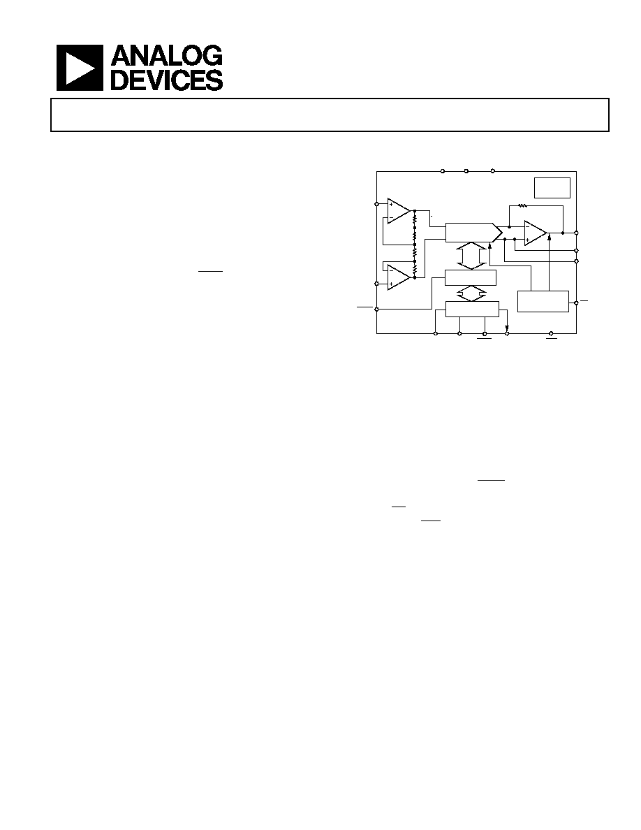
FUNCTIONAL BLOCK DIAGRAM
V
OUT
V
DD
DGND
AD5570
REFIN
REFGND
LDAC
SDIN
CLR
SCLK
SYNC
PD
DAC REGISTER
SHIFT REGISTER
POWER-DOWN
CONTROL LOGIC
POWER-ON
RESET
SDO
V
SS
R
AGND
AGNDS
R
R
R
16-BIT
DAC
03760-0-001
Figure 1.
GENERAL DESCRIPTION
The AD5570 is a single 16-bit serial input, voltage output DAC
that operates from supply voltages of ±12 V up to ±15 V.
Integral linearity (INL) and differential nonlinearity (DNL) are
accurate to 1 LSB. During power-up (when the supply voltages
are changing), V
OUT
is clamped to 0 V via a low impedance path.
The AD5570 DAC comes complete with a set of reference
buffers. The reference buffers allow a single, positive reference
to be used. The voltage on REFIN is gained up and inverted
internally to give the positive and negative reference for the
DAC core. Having the reference buffers on-chip eliminates the
need for external components such as inverters, precision
amplifiers, and resistors, thereby reducing the overall solution
size and cost.
The AD5570 uses a versatile 3-wire interface that is compatible
with SPIÆ, QSPITM, MICROWIRETM, and DSPÆ interface standards.
Data is presented to the part in the format of a 16-bit serial
word. Serial data is available on the SDO pin for daisy-chaining
purposes. Data readback allows the user to read the contents of
the DAC register via the SDO pin.
Features on the AD5570 include LDAC, which may be used to
update the output of the DAC. The device also has a power-
down pin (PD), which allows the DAC to be put into a low
power state, and a CLR pin that allows the output to be cleared
to 0 V.
The AD5570 is available in a 16-lead SSOP package.
PRODUCT HIGHLIGHTS
1. 1 LSB maximum INL and DNL.
2. Buffered voltage output up to ±14 V.
3. Output controlled during power-up.
4. On-board reference buffers.
5. Wide temperature range of -40∞C to +125∞C.

AD5570
Rev. 0 | Page 2 of 24
TABLE OF CONTENTS
Specifications..................................................................................... 3
Standalone Timing Characteristics ................................................ 4
Daisy Chaining and Readback Timing Characteristics............... 6
Absolute Maximum Ratings............................................................ 8
ESD Caution.................................................................................. 8
Pin Configuration and Function Descriptions............................. 9
Terminology .................................................................................... 10
Typical Performance Characteristics ........................................... 11
General Description ....................................................................... 16
DAC Architecture....................................................................... 16
Reference Buffers........................................................................ 16
Serial Interface ............................................................................ 16
Transfer Function ....................................................................... 17
CLEAR (
CLR
)............................................................................. 17
Power-Down (
PD
) ..................................................................... 17
Power-On Reset.......................................................................... 17
Serial Data Output (SDO)......................................................... 17
Applications Information .............................................................. 19
Typical Operating Circuit ......................................................... 19
Layout Guidelines....................................................................... 20
Opto-Coupler Interface ............................................................. 20
Microprocessor Interfacing....................................................... 20
Evaluation Board ........................................................................ 22
Outline Dimensions ....................................................................... 24
Ordering Guide .......................................................................... 24
REVISION HISTORY
Revision 0: Initial Version
AD5570
Rev. 0 | Page 3 of 24
SPECIFICATIONS
V
DD
= +11.4 V to +16.5 V; V
SS
= -11.4 V to -16.5 V; V
REF
= 5 V; REFGND = GND = 0 V; R
L
= 5 k and C
L
= 200 pF to GND; all
specifications T
MIN
to T
MAX
, unless otherwise noted.
Table 1.
A/W
Grade
1, 2
B/Y Grade
2
Parameter
Min Typ
3
Max Min
Typ
3
Max
Unit Test
Conditions/Comments
ACCURACY
Resolution *
16
Bits
Monotonicity *
16
Bits
Relative Accuracy (INL)
±0.6
±0.4
±1
LSB
At 25∞C
±0.6
±2
-1
±0.4
+1.25
LSB
Differential Nonlinearity
(DNL)
* *
* -1
±0.3 +1
LSB
Negative Full-Scale Error
*
*
±0.9
±7.5
mV
Full-Scale Error
*
*
±1.8
± 6
mV
Bipolar Zero Error
*
*
±0.9
±7.5
mV
Gain Error
*
*
±1.8
±7.5
mV
Gain Temperature
Coefficient
4
* *
0.25
±1.5
ppm
FSR/∞C
REFERENCE INPUT
Reference Input Range
4
*
*
*
4
5
5
V
With ±11.4 V supplies
*
*
*
4
5
7
V
With ±16.5 V supplies
Input Current
*
±0.1
µA
OUTPUT CHARACTERISTICS
4
Output Voltage Range
*
*
V
SS
+ 1.4 V
V
DD
- 1.4 V
V
±11.4 V supplies
*
*
V
SS
+ 2.5 V
V
DD
- 2.5 V
V
±16.5 V supplies
Output Voltage Settling Time
*
*
12
16
µs
At 16 bits to ±0.5 LSB
*
*
10
13
µs
To
0.003%
*
*
6
7
µs
512 LSB code change
Slew Rate
*
6.5
V/µs
Measured from 10% to 90%
Digital-to-Analog Glitch
Impulse
*
15
nV-s
±12 V supplies; 1 LSB change
around the major carry
Bandwidth
*
20
kHz
Short Circuit Current
*
25
mA
Output Noise Voltage Density
*
85
nV/Hz
f = 1 kHz; midscale loaded
DAC Output Impedance
4
* *
0.35
0.5
Digital Feedthrough
*
0.5
nV-s
WARMUP TIME
5
*
12
s
LOGIC INPUTS
Input Current
*
±0.1
µA
V
INH
, Input High Voltage
*
2
V
V
INL
, Input Low Voltage
*
0.8
V
C
IN
, Input Capacitance
4
*
3
pF
LOGIC OUTPUTS
V
OL
, Output Low Voltage
*
0.4
V
I
SINK
= 1 mA
Floating-State Output
Capacitance
*
8
pF

AD5570
Rev. 0 | Page 4 of 24
A/W
Grade
1, 2
B/Y Grade
2
Parameter
Min Typ
3
Max Min
Typ
3
Max
Unit Test
Conditions/Comments
POWER REQUIREMENTS
V
DD
/V
SS
*
* ±11.4
±16.5
V
I
DD
*
4 5
mA V
OUT
unloaded
I
SS
*
3.5 5
mA V
OUT
unloaded
Power-Down Current
*
16
µA
V
OUT
unloaded
Power Supply Sensitivity
6
*
0.1
LSB/V ±15 V supplies ±10%;
full scale loaded
Power Dissipation
*
100
mW
V
OUT
unloaded
1
Asterisk (*) = specifications same as B/Y grade.
2
Temperature range: A and B = -40∞C to +85∞C; W and Y = ≠40∞C to +125∞C.
3
Typical specifications at ±12 V/±15 V, 25∞C.
4
Guaranteed by design.
5
Warmup time is required for the device to reach thermal equilibrium, thus achieving rated performance.
6
Sensitivity of negative full-scale error and positive full-scale error to V
DD
, V
SS
variations.

AD5570
Rev. 0 | Page 5 of 24
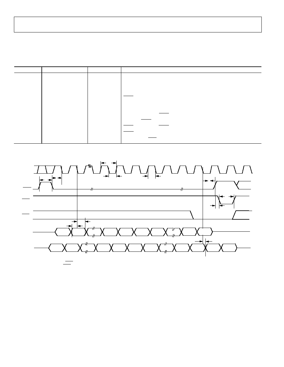
STANDALONE TIMING CHARACTERISTICS
V
DD
= +12 V ± 5%, V
SS
= -12 V ± 5% or V
DD
= +15 V ± 10%, V
SS
= -15 V ± 10%; V
REF
= 5 V; REFGND = GND = 0 V; R
L
= 5 k;
and C
L
= 200 pF to GND; all specifications T
MIN
to T
MAX
, unless otherwise noted.
Table 2.
Parameter
Limit at T
MIN
, T
MAX
Unit
Description
f
MAX
10
MHz max
SCLK frequency
t
1
100
ns min
SCLK cycle time
t
2
35
ns min
SCLK high time
t
3
35
ns min
SCLK low time
t
4
10 ns
min
SYNC to SCLK falling edge setup time
t
5
35
ns min
Data setup time
t
6
0
ns min
Data hold time
t
7
45 ns
min
SCLK falling edge to SYNC rising edge
t
8
45 ns
min
Minimum SYNC high time
t
9
0 ns
min
SYNC rising edge to LDAC falling edge
t
10
50 ns
min
LDAC pulse width
t
11
0 ns
min
LDAC falling edge to SYNC falling edge (no update)
t
12
0 ns
min
LDAC rising edge to SYNC rising edge (no update)
t
13
20 ns
min
CLR pulse width
All parameters guaranteed by design and characterization. Not production tested.
All input signals are measured with tr = tf = 5 ns (10% to 90% of V
DD
) and timed from a voltage level of (V
IL
+V
IH
)/2.
DB15
DB0
SCLK
SYNC
SDIN
LDAC
1
CLR
LDAC
2
NOTES
1. ASYNCHRONOUS LDAC UPDATE MODE. UPDATE ON FALLING EDGE OF LDAC.
2. SYNCHRONOUS LDAC UPDATE MODE. UPDATE ON RISING EDGE OF SYNC.
t
3
t
2
t
5
t
6
t
7
t
9
t
1
t
4
t
8
t
12
t
11
t
10
t
13
03760-0-002
Figure 2. Serial Interface Timing Diagram
AD5570
Rev. 0 | Page 6 of 24
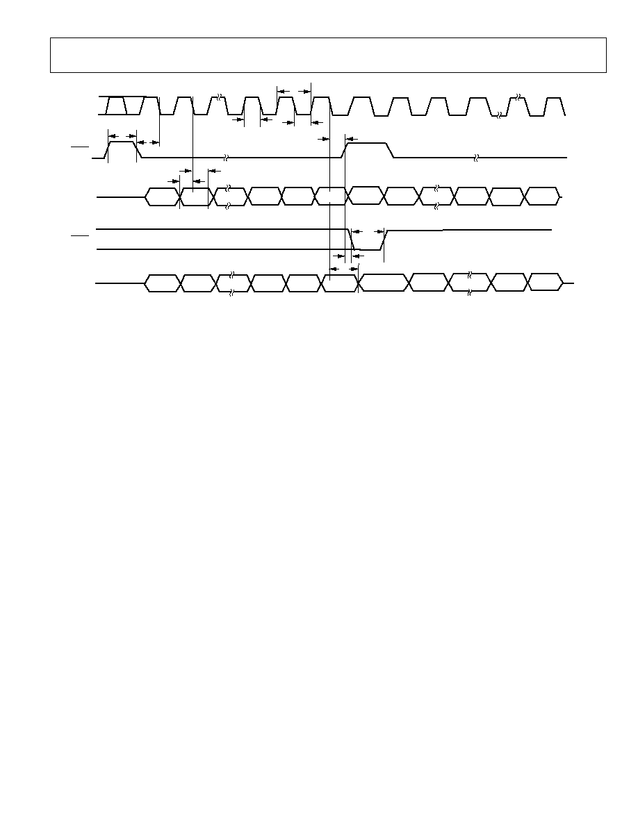
DAISY-CHAINING AND READBACK TIMING CHARACTERISTICS
V
DD
= +12 V ± 5%, V
SS
= -12 V ± 5% or V
DD
= +15 V ± 10%, V
SS
= -15 V ± 10%; V
REF
= 5 V; REFGND = GND = 0 V; R
L
= 5 k,
and C
L
= 200 pF to GND; all specifications T
MIN
to T
MAX
, unless otherwise noted.
Table 3.
Parameter
Limit at T
MIN
, T
MAX
Unit
Description
f
MAX
2
MHz max
SCLK frequency
t
1
500
ns min
SCLK cycle time
t
2
200
ns min
SCLK high time
t
3
200
ns min
SCLK low time
t
4
10 ns
min
SYNC to SCLK falling edge setup time
t
5
35
ns min
Data setup time
t
6
0
ns min
Data hold time
t
7
45 ns
min
SCLK falling edge to SYNC rising edge
t
8
45 ns
min
Minimum SYNC high time
t
9
0 ns
min
SYNC rising edge to LDAC falling edge
t
10
50 ns
min
LDAC pulse width
t
14
1
200 ns
max
Data delay on SDO
All parameters guaranteed by design and characterization. Not production tested.
All input signals are measured with tr = tf = 5 ns (10% to 90% of V
DD
) and timed from a voltage level of (V
IL
+V
IH
)/2.
SDO; R
PULLUP
= 5 k, C
L
= 15 pF.
1
With C
L
= 0 pF, t
15
= 100 ns.
SCLK
SYNC
SDIN
DB15 (N)
DB15 (N)
DB0 (N)
DB0 (N)
DB15
(N+1)
DB15
(N+1)
DB0
(N+1)
LDAC
1
SDO
LDAC
2
NOTES
1. ASYNCHRONOUS LDAC UPDATE MODE
2. SYNCHRONOUS LDAC UPDATE MODE
t
1
t
8
t
10
t
2
t
3
t
4
t
6
t
5
t
9
t
7
t
14
03760-0-003
Figure 3. Daisy-Chaining Timing Diagram
AD5570
Rev. 0 | Page 7 of 24
SCLK
SYNC
SDIN
SDO
LDAC
DB15 (N)
DB0 (N)
DB0 (N)
DB14 (N)
DB15 (N)
DB15
(N+1)
DB0
(N+1)
t
2
t
3
t
6
t
5
t
7
t
9
t
1
t
10
t
14
t
8
t
4
03760-0-004
Figure 4. Readback Timing Diagram
AD5570
Rev. 0 | Page 8 of 24
ABSOLUTE MAXIMUM RATINGS
T
A
= 25∞C, unless otherwise noted.
Table 4.
Parameter Rating
V
DD
to AGND, AGNDS, DGND
-0.3 V, +17 V
V
SS
to AGND, AGNDS, DGND
+0.3 V, -17 V
AGND, AGNDS to DGND
-0.3 V to +0.3 V
REFGND to AGND, ADNDS
V
SS
- 0.3 V to V
DD
+ 0.3 V
REFIN to AGND, AGNDS
V
SS
- 0.3 V to V
DD
+ 0.3 V
REFIN to REFGND
-0.3 V to +17 V
Digital Inputs to DGND
-0.3 V to V
DD
+ 0.3 V
V
OUT
to AGND, AGNDS
-0.3 V to V
DD
+ 0.3 V
SDO to DGND
-0.3 V to +6.5 V
Operating Temperature Range:
-40∞C to +125∞C
W, Y Grades
-40∞C to +125∞C
A, B Grades
-40∞C to +85∞C
Storage Temperature Range
-65∞C to +150∞C
Maximum Junction Temperature
(T
J
Max)
150∞C
16-Lead SSOP Package
Power Dissipation
(T
J
max ≠ T
A
)/
JA
JA
Thermal Impedance
139∞C/W
Lead Temperature (Soldering 10 s)
300∞C
IR Reflow, Peak Temperature
230∞C
Stresses above those listed under Absolute Maximum Ratings
may cause permanent damage to the device. This is a stress
rating only and functional operation of the device at these or
any other conditions above those listed in the operational
sections of this specification is not implied. Exposure to
absolute maximum rating conditions for extended periods may
affect device reliability.
ESD CAUTION
ESD (electrostatic discharge) sensitive device. Electrostatic charges as high as 4000 V readily accumulate on
the human body and test equipment and can discharge without detection. Although this product features
proprietary ESD protection circuitry, permanent damage may occur on devices subjected to high energy
electrostatic discharges. Therefore, proper ESD precautions are recommended to avoid performance
degradation or loss of functionality.
AD5570
Rev. 0 | Page 9 of 24
PIN CONFIGURATION AND FUNCTION DESCRIPTIONS
V
SS
1
V
DD
2
CLR
3
LDAC
4
SYNC
5
SCLK
6
SDIN
7
SDO
8
REFGND
REFIN
REFGND
V
OUT
AGNDS
16
15
14
13
12
AGND
PD
DGND
11
10
9
AD5570
TOP VIEW
(Not to Scale)
03760-0-005
Figure 5. 16-Lead SSOP Pin Configuration (RS-16)
Table 5. Pin Function Descriptions
Pin No.
Mnemonic
Description
1 V
SS
Negative Analog Supply Voltage. -12 V ± 5% to -15 V ± 10% for specified performance.
2 V
DD
Positive Analog Supply Voltage. 12 V ± 5% to 15 V ± 10% for specified performance.
3
CLR
Level Sensitive, Active Low Input. A falling edge of CLR resets V
OUT
to AGND. The contents of the registers are
untouched.
4
LDAC
Active Low Control Input. Transfers the contents of the input register to the DAC register. LDAC may be tied
permanently low, enabling the outputs to be updated on the rising edge of SYNC.
5
SYNC
Active Low Control Input. This is the frame synchronization signal for the data. When SYNC goes low, it powers
on the SCLK and SDIN buffers and enables the input shift register. Data is transferred in on the falling edges of
the following 16 clocks.
6 SCLK Serial Clock Input. Data is clocked into the input register on the falling edge of the serial clock input. Data can
be transferred at rates of up to 8 MHz.
7 SDIN Serial Data Input. This device has a 16-bit register. Data is clocked into the register on the falling edge of the
serial clock input.
8 SDO
Serial Data Output. Can be used for daisy chaining a number of devices together or for reading back the data in
the shift register for diagnostic purposes. This is an open-drain output; it should be pulled to logic high with an
external pull-up resistor of ~5 k.
9
DGND
Digital Ground. Ground reference for all digital circuitry.
10
PD
Active Low Control Input. Allows the DAC to be put into a power-down state.
11
AGND
Analog Ground. Ground reference for all analog circuitry.
12
AGNDS
Analog Ground Sense. This is normally tied to AGND.
13
V
OUT
Analog Output Voltage.
14
REFGND
This pin should be tied to 0 V.
15
REFIN
Voltage Reference Input. This is internally buffered before being applied to the DAC. For bipolar ±10 V output
range, REFIN is 5 V.
16
REFGND
This pin should be tied to 0 V.

AD5570
Rev. 0 | Page 10 of 24
TERMINOLOGY
Relative Accuracy or Integral Nonlinearity (INL)
Relative accuracy or integral nonlinearity is a measure of the
maximum deviation, in LSBs, from a straight line passing
through the endpoints of the DAC transfer function.
Monotonicity
A DAC is monotonic, if the output either increases or remains
constant for increasing digital inputs. The AD5570 is monotonic
over its full operating temperature range.
Differential Nonlinearity (DNL)
Differential nonlinearity is the difference between the measured
change and the ideal 1 LSB change between any two adjacent
codes. A specified differential nonlinearity of ±1 LSB maximum
ensures monotonicity.
Gain Error
Gain error is the difference between the actual and ideal analog
output range, expressed as a percent of the full-scale range. It is
the deviation in slope of the DAC transfer characteristic from
the ideal.
Gain Error Temperature Coefficient
Gain error temperature coefficient is a measure of the change in
gain error with changes in temperature. It is expressed in
ppm/∞C.
Negative Full-Scale Error / Zero Scale Error
Negative full-scale error is the error in the DAC output voltage
when all 0s are loaded into the DAC latch. Ideally, the output
voltage, with all 0s in the DAC latch, should be -2 V
REF
.
Full-Scale Error
Full-scale error is the error in the DAC output voltage when all
1s are loaded to the DAC latch. Ideally the output voltage, with
all 1s loaded into the DAC latch, should be 2 V
REF
- 1 LSB.
Bipolar Zero Error
Bipolar zero error is the deviation of the analog input from the
ideal half-scale output of 0.0000 V when the inputs are loaded
with 0x8000.
Output Voltage Settling Time
Output voltage settling time is the amount of time it takes for
the output to settle to a specified level for a full-scale input
change.
Slew Rate
The slew rate of a device is a limitation in the rate of change of
output voltage. The output slewing speed of a voltage-output
D/A converter is usually limited by the slew rate of the amplifier
used at its output. Slew rate is measured from 10% to 90% of the
output signal and is given in V/µs.
Digital-to-Analog Glitch Impulse
Digital-to-analog glitch impulse is the amount of charge in-
jected into the analog output when the input codes in the DAC
register change state. It is specified as the area of the glitch in
nV-s and is measured when the digital input code changes by
1 LSB at the major carry transition, that is, from code 0x7FFF to
0x8000.
Bandwidth
The reference amplifiers within the DAC have a finite band-
width to optimize noise performance. To measure it, a sine
wave is applied to the reference input (REFIN), with full-scale
code loaded to the DAC. The bandwidth is the frequency at
which the output amplitude falls to 3 dB below the input.
Digital Feedthrough
Digital feedthrough is a measure of the impulse injected into
the analog output of the DAC from the digital inputs of the
DAC, but is measured when the DAC output is not updated.
SYNC is held high, while the CLK and SDIN signals are toggled.
It is specified in nV-s and is measured with a full-scale code
change on the data bus, that is, from all 0s to all 1s and vice
versa.
Power Supply Sensitivity
Power supply sensitivity indicates how the output of the DAC is
affected by changes in the power supply voltage.
AD5570
Rev. 0 | Page 11 of 24
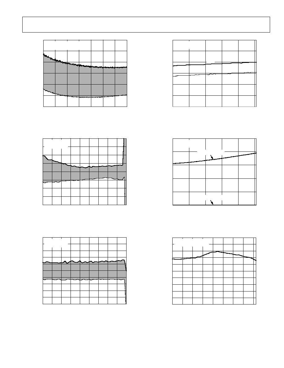
TYPICAL PERFORMANCE CHARACTERISTICS
CODE
INL (
L
SB)
0
≠1.0
≠0.8
≠0.6
≠0.4
≠0.2
0
0.2
1.0
0.6
0.4
0.8
50k
40k
30k
20k
10k
60k
03760-0-006
T
A
= 25∞C
V
DD
/V
SS
= ±15V
REFIN = 5V
Figure 6. Integral Nonlinearity vs. Code, V
DD
/V
SS
= ±15 V
CODE
DNL (LS
B
)
0
≠1.0
≠0.8
≠0.6
≠0.4
≠0.2
0
0.2
1.0
0.6
0.4
0.8
50k
40k
30k
20k
10k
60k
03760-0-007
T
A
= 25∞C
V
DD
/V
SS
= ±15V
REFIN = 5V
Figure 7. Differential Nonlinearity vs. Code, V
DD
/V
SS
= ±15 V
CODE
INL (
L
SB)
0
≠1.0
≠0.8
≠0.6
≠0.4
≠0.2
0
0.2
1.0
0.6
0.4
0.8
50k
40k
30k
20k
10k
60k
03760-0-008
T
A
= 25∞C
V
DD
/V
SS
= ±12V
REFIN = 5V
Figure 8. Integral Nonlinearity vs. Code, V
DD
/V
SS
= ±12 V
CODE
DNL (LS
B
)
0
≠1.0
≠0.8
≠0.6
≠0.4
≠0.2
0
0.2
1.0
0.6
0.4
0.8
50k
40k
30k
20k
10k
60k
03760-0-009
T
A
= 25∞C
V
DD
/V
SS
= ±12V
REFIN = 5V
Figure 9. Differential Nonlinearity vs. Code, V
DD
/V
SS
= ±12 V
TEMPERATURE (∞C)
INL (LSB)
≠40
≠1.0
≠0.8
≠0.6
≠0.4
≠0.2
0
0.2
1.0
0.8
0.4
0.6
100
80
60
40
20
0
≠20
120
03760-0-018
V
DD
/V
SS
= ±15V
REFIN = 5V
Figure 10. Integral Nonlinearity vs. Temperature, ±15 V Supplies
TEMPERATURE (∞C)
DNL (LS
B
)
≠40
≠1.0
≠0.8
≠0.6
≠0.4
≠0.2
0
0.2
1.0
0.8
0.4
0.6
100
80
60
40
20
0
≠20
120
03760-0-019
V
DD
/V
SS
= ±15V
REFIN = 5V
Figure 11. Differential Nonlinearity vs. Temperature, ±15 V Supplies
AD5570
Rev. 0 | Page 12 of 24
TEMPERATURE (∞C)
IN
L (
L
SB
)
≠40
≠1.0
≠0.8
≠0.6
≠0.4
≠0.2
0
0.2
1.0
0.8
0.4
0.6
100
80
60
40
20
0
≠20
120
03760-0-020
V
DD
/V
SS
= ±12V
REFIN = 5V
Figure 12. Integral Nonlinearity vs. Temperature, ±12 V Supplies
TEMPERATURE (∞C)
DNL (LS
B
)
≠40
≠1.0
≠0.8
≠0.6
≠0.4
≠0.2
0
0.2
1.0
0.8
0.4
0.6
100
80
60
40
20
0
≠20
120
03760-0-021
V
DD
/V
SS
= ±12V
REFIN = 5V
Figure 13. Differential Nonlinearity vs. Temperature, ±12 V Supplies
SUPPLY VOLTAGE (V)
INL (
L
SB)
11.4
15.0
14.0
13.0
12.0
16.0 16.5
03760-0-023
≠1.0
≠0.6
≠0.4
≠0.2
≠0.8
0.2
0.4
0
1.0
0.6
0.8
T
A
= 25∞C
REFIN = 5V
Figure 14. Integral Nonlinearity vs. Supply Voltage
SUPPLY VOLTAGE (V)
DNL (LS
B
)
11.4
15.0
14.0
13.0
12.0
16.0 16.5
03760-0-024
≠1.0
≠0.6
≠0.4
≠0.2
≠0.8
0.2
0.4
0
1.0
0.6
0.8
T
A
= 25∞C
REFIN = 5V
Figure 15. Differential Nonlinearity vs. Supply Voltage
REFERENCE VOLTAGE (V)
INL E
RROR (LS
B
)
2.0
≠1.0
≠0.5
0
0.5
1.0
2.0
1.5
4.5
4.0
3.5
3.0
2.5
5.0
5.5
03760-0-026
V
DD
/V
SS
= ±12V
T
A
= 25∞C
Figure 16. Integral Nonlinearity Error vs. Reference Voltage, ±12 V Supplies
REFERENCE VOLTAGE (V)
DNL E
RROR (LS
B
)
2.0
≠0.5
≠0.3
≠0.2
≠0.1
≠0.4
0
0.1
0.2
0.3
0.5
0.4
4.5
4.0
3.5
3.0
2.5
5.0
5.5
03760-0-027
V
DD
/V
SS
= ±12V
T
A
= 25∞C
Figure 17. Differential Nonlinearity Error vs. Reference Voltage,
±12 V Supplies
AD5570
Rev. 0 | Page 13 of 24
REFERENCE VOLTAGE (V)
TU
E ER
R
O
R
(
L
SB
)
2.0
≠5.0
≠2.5
0
2.5
5.0
10.0
7.5
4.5
4.0
3.5
3.0
2.5
5.0
5.5
03760-0-028
V
DD
/V
SS
= ±15V OR ±12V
T
A
= 25∞C
Figure 18. TUE Error vs. Reference Voltage
REFERENCE VOLTAGE (V)
INL ERROR (LSB)
2.0
2.5
≠2.0
≠1.5
≠1.0
≠0.5
0
0.5
1.0
1.5
2.0
3.5
3.0
5.0
5.5
6.0
4.5
4.0
6.5
03760-0-048
V
DD
/V
SS
= ±15V
T
A
= 25∞C
Figure 19. Integral Nonlinearity Error vs. Reference Voltage, ± 15 V Supplies
REFERENCE VOLTAGE (V)
INL E
RROR (LS
B
)
2.0
2.5
≠1.0
≠0.8
≠0.6
≠0.4
≠0.2
0
0.2
0.4
0.6
0.8
1.0
3.5
3.0
5.0
5.5
6.0
4.5
4.0
6.5
03760-0-049
V
DD
/V
SS
= ±15V
T
A
= 25∞C
Figure 20. Differential Nonlinearity Error vs. Reference Voltage,
± 15 V Supplies
V
DD
/V
SS
(V)
|I
SS
|
CURRE
NT (mA)
11.4
2.0
2.5
3.0
3.5
4.0
5.0
4.5
14.4
13.4
12.4
15.4
16.4
03760-0-029
|I
DD
|
T
A
= 25∞C
REFIN = 5V
Figure 21. I
DD
/I
SS
vs.V
DD
/V
SS
I
DD
/I
SS
(V)
P
O
WE
R-DOWN CURRE
N
T (
µ
A)
11.4
0
5
10
15
25
20
14.4
13.4
12.4
15.4
16.4
03760-0-030
|I
SS IN POWER-DOWN
|
|I
DD IN POWER-DOWN
|
T
A
= 25∞C
REFIN = 5V
Figure 22. I
DD
/I
SS
in Power-Down vs. Supply Voltage
TEMPERATURE (∞C)
OFFSET ER
R
O
R
(
L
SB
)
≠40
≠10
≠9
≠8
≠7
≠6
≠5
≠4
0
≠1
≠3
≠2
100
80
60
40
20
0
≠20
120
03760-0-031
V
DD
/V
SS
= ±12V OR ±15V
REFIN = 5V
Figure 23. Offset Error vs. Temperature

AD5570
Rev. 0 | Page 14 of 24
TEMPERATURE (∞C)
BIP
O
LAR ZE
RO E
RROR (LS
B
)
≠40
≠10
≠9
≠8
≠7
≠6
≠5
≠4
0
≠1
≠3
≠2
100
80
60
40
20
0
≠20
120
03760-0-032
V
DD
/V
SS
= ±12V
V
DD
/V
SS
= ±15V
REFIN = 5V
Figure 24. Bipolar Zero Error vs. Temperature
TEMPERATURE (∞C)
GAIN E
RROR (LS
B
)
≠40
≠10
≠8
≠6
≠4
≠2
0
2
10
0
4
6
100
80
60
40
20
0
≠20
120
03760-0-034
V
DD
/V
SS
= ±12V
V
DD
/V
SS
= ±15V
REFIN = 5V
Figure 25. Gain Error vs. Temperature
V
LOGIC
(V)
I
DD
(mA)
0
0.5
1.0
1.5
2.0
2.5
3.0
3.5
4.0
4.5
3.75
3.80
3.85
3.90
3.95
4.00
4.05
4.10
4.15
5.0
03760-0-035
T
A
= 25∞C
REFIN = 5V
15V SUPPLIES
DECREASING
INCREASING
12V SUPPLIES
INCREASING
DECREASING
Figure 26. Supply Current vs. Logic Input Current for SCLK, SYNC, SDIN,
and LDAC Increasing and Decreasing
≠10.0
≠4.0
≠6.0
≠8.0
4.0
2.0
0
≠2.0
11.0
10.0
8.0
6.0
1
µ
s/DIV
V
DD
= +15V
V
SS
= ≠15V
REFIN = 5V
T
A
= 25∞C
03760-0-046
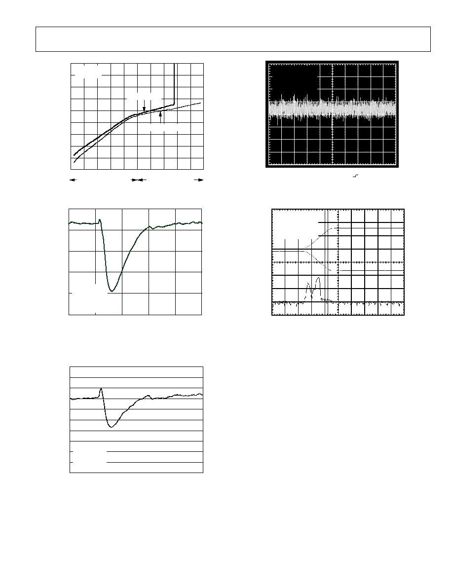
Figure 27. Settling Time
CAPACITANCE (nF)
TIME (
µ
s)
0
1
2
3
4
5
6
7
8
9
0
5
10
15
20
25
30
35
40
9.4
03760-0-037
T
A
= 25∞C
REFIN = 5V
V
DD
/V
SS
= ±12V
V
DD
/V
SS
= ±15V
Figure 28.14-Bit Settling Time vs. Load Capacitance
SINK CURRENT (mA)
SOURCE CURRENT (mA)
OUTPUT VOLTAGE (V)
≠10
≠8
≠6
≠4
≠2
0
2
4
6
8
9.9952
9.9955
9.9958
9.9961
9.9964
9.9967
9.9970
9.9973
9.9976
9.9979
9.9982
9.9985
9.9988
9.9991
9.9994
9.9997
10.0000
10
03760-0-038
15V SUPPLIES
12V SUPPLIES
T
A
= 25∞C
REFIN = 5V
Figure 29. Source and Sink Capability of Output Amplifier
with Full Scale Loaded
AD5570
Rev. 0 | Page 15 of 24
OUTPUT VOLTAGE (V)
≠10
≠8
≠6
≠4
≠2
0
2
4
6
8
≠10.0000
≠9.9997
≠9.9994
≠9.9991
≠9.9988
≠9.9985
≠9.9982
≠9.9979
≠9.9976
≠9.9973
10
03760-0-039
12V SUPPLIES
15V SUPPLIES
SINK CURRENT (mA)
SOURCE CURRENT (mA)
T
A
= 25∞C
REFIN = 5V
Figure 30. Source and Sink Capability of Output Amplifier
with Zero Scale Loaded
1
µ
s/DIV
V
OUT
(V
)
≠0.10
≠0.09
≠0.08
≠0.07
≠0.06
≠0.05
V
DD
= +15V
V
SS
= ≠15V
REFIN = 5V
T
A
= 25∞C
7 FFF
8000H
03760-0-040
Figure 31. Major Code Transition Glitch Energy, ±15 V Supplies
1
µ
s (DIV)
VOLTA
G
E (
V
)
≠0.072
≠0.067
≠0.062
≠0.057
≠0.052
≠0.047
≠0.042
≠0.037
≠0.032
≠0.027
≠0.022
V
DD
= +12V
V
SS
= ≠12V
REFIN = 5V
T
A
= 25∞C
8000
7FFFH
03760-0-051
Figure 32. Major Code Transition Glitch Energy, ±12 V Supplies
CH1 20
µ
V/DIV
20
µ
s/PT
M 1.0
ms 500kS/s
A CH1 0.0V
03760-0-047
V
DD
= +15V
V
SS
= ≠15V
MIDSCALE LOADED
20
µ
V/DIV
V
REFIN
= 0V
Figure 33. Peak-to-Peak Noise (100 kHz Bandwidth)
V
DD
= +15V
V
SS
= ≠15V
REFIN = 5V
T
A
= 25∞C
RAMP TIME = 100
µ
s
V
DD
/V
SS
= 10V/DIV
V
OUT
= 10mV/DIV
100
µ
s/DIV
V
OUT
V
SS
V
DD
03760-0-042
Figure 34. V
OUT
vs. V
DD
/V
SS
on Power-Up
AD5570
Rev. 0 | Page 16 of 24
GENERAL DESCRIPTION
The AD5570 is a single 16-bit, serial input, voltage output DAC.
It operates from supply voltages of ±11.4 V to ±16.5 V, and has a
buffered voltage output of up to ±13.6 V. Data is written to the
AD5570 in a 16-bit word format, via a 3-wire serial interface.
The device also offers an SDO pin, which is available for daisy
chaining or readback.
The AD5570 incorporates a power-on reset circuit, which
ensures that the DAC output powers up to 0 V. The device also
has a power-down pin, which reduces the typical current
consumption to 16 µA.
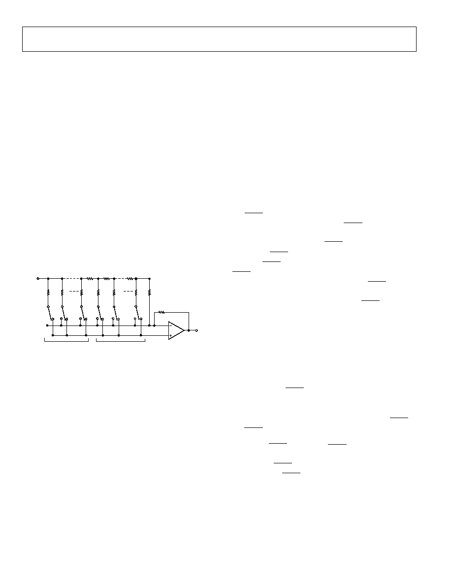
DAC ARCHITECTURE
The DAC architecture of the AD5570 consists of a 16-bit
current-mode segmented R-2R DAC. The simplified circuit
diagram for the DAC section is shown in Figure 35.
The four MSBs of the 16-bit data word are decoded to drive
15 switches, E1 to E15. Each of these switches connects one of
the 15 matched resistors to either AGND or IOUT. The remain-
ing 12 bits of the data word drive switches S0 to S11 of the
12-bit R-2R ladder network.
2R
E15
Vref
2R
E14
E1
2R
S11
R
R
R
2R
S10
2R
12 BIT R-2R LADDER
V
OUT
2R
S0
2R
AGND
R/8
4 MSBs DECODED INTO
15 EQUAL SEGMENTS
03760-
0-
010
Figure 35. DAC Ladder Structure
REFERENCE BUFFERS
The AD5570 operates with an external reference. The reference
input (REFIN) has an input range of up to 7 V. This input
voltage is then used to provide a buffered positive and negative
reference for the DAC core. The positive reference is given by
REFIN
REF
V
2
V
◊
=
+
while the negative reference to the DAC core is given by
REFIN
REF
V
2
V
◊
=
-
These positive and negative reference voltages define the DAC
output range.
SERIAL INTERFACE
The AD5570 is controlled over a versatile 3-wire serial interface
that operates at clock rates up to 10 MHz and is compatible with
SPI, QSPI, MICROWIRE, and DSP interface standards.
Input Shift Register
The input shift register is 16 bits wide. Data is loaded into the
device as a 16-bit word under the control of a serial clock input,
SCLK. The timing diagram for this operation is shown in
Figure 2.
Upon power-up, the input shift register and DAC register are
loaded with midscale (0x8000). The DAC coding is straight
binary; all 0s produce an output of -2 V
REF
; all 1s produce an
output of +2 V
REF
- 1 LSB.
The SYNC input is a level-triggered input that acts as a frame
synchronization signal and chip enable. SYNC must frame the
serial word being loaded into the device. Data can be trans-
ferred into the device only while SYNC is low. To start the serial
data transfer, SYNC should be taken low, observing the
minimum SYNC to SCLK falling edge setup time, t
4
. After
SYNC goes low, serial data on SDIN is shifted into the device's
input shift register on the falling edges of SCLK. SYNC may be
taken high after the falling edge of the 16th SCLK pulse,
observing the minimum SCLK falling edge to SYNC rising edge
time, t
7
.
After the end of the serial data transfer, data is automatically
transferred from the input shift register to the input register of
the DAC.
When data has been transferred into the input register of the
DAC, the DAC register and DAC output can be updated by
taking LDAC low while SYNC is high.
Load DAC Input (LDAC)
When data has been transferred into the input register of the
DAC, there are two ways in which the DAC register and DAC
output can be updated. Depending on the status of both SYNC
and LDAC, one of two update modes is selected.
Synchronous LDAC: In this mode, LDAC is low while data is
being clocked into the input shift register. The DAC output is
updated when SYNC is taken high. The update here occurs on
the rising edge of SYNC.

AD5570
Rev. 0 | Page 17 of 24
Asynchronous LDAC: In this mode, LDAC is high while data is
being clocked in. The DAC output is updated by taking LDAC
low any time after SYNC has been taken high. The update now
occurs on the falling edge of LDAC.
Figure 36 shows a simplified block diagram of the input loading
circuitry.
V
OUT
DAC
REGISTER
INPUT SHIFT
REGISTER
OUTPUT
I/V AMPLIFIER
LDAC
SDO
SDIN
16-BIT
DAC
V
REFIN
SYNC
03760-0-012
Figure 36. Simplified Serial Interface Showing Input Loading Circuitry
TRANSFER FUNCTION
Table 6 shows the ideal input code to output voltage relationship
for the AD5570.
Table 6. Binary Code Table
Digital Input
Analog Output
MSB
LSB V
OUT
1111 1111 1111 1111 +2
V
REF
◊ (32,767/32,768)
1000 0000 0000 0001 +2
V
REF
◊ (1/32,768)
1000 0000 0000 0000 0
V
0111 1111 1111 1111 -2
V
REF
◊ (1/32,768)
0000 0000
0000 0000 -2
V
REF
The output voltage expression is given by
]
65536
/
[
4
2
D
V
V
V
REFIN
REFIN
OUT
◊
+
-
=
where:
D is the decimal equivalent of the code loaded to the DAC.
V
REFIN
is the reference voltage available at the REFIN pin.
CLEAR (CLR)
CLR is an active low digital input that allows the output to be
cleared to 0 V. When the CLR signal is brought back high, the
output stays at 0 V until LDAC is brought low. The relationship
between LDAC and CLR is explained further in Table 7.
Table 7. Relationships among PD, CLR, and LDAC
PD
CLR
LDAC
Comments
0 x x
PD has priority over LDAC and CLR. The
output remains at 0 V through an internal
20 k resistor. It is still possible to address
both the input register and DAC register
when the AD5570 is in power-down.
1 0 0
Data is written to the input register and
DAC register. CLR has higher priority over
LDAC; therefore, the output is at 0 V.
1 0 1
Data is written to the input register only.
The output is at 0 V and remains at 0 V,
when CLR is taken back high.
1 1 0
Data is written to the input register and
the DAC register. The output is driven to
the DAC level.
1 1 1
Data is written to the input register only.
The output of the DAC register is
unchanged.
POWER-DOWN (PD)
The power-down pin allows the user to place the AD5570 into a
power-down mode. When in this mode, power consumption is
at a minimum; the device consumes only 16 µA typically.
POWER-ON RESET
The AD5570 contains a power-on reset circuit that controls the
output during power-up and power-down. This is useful in
applications where the known state of the output of the DAC
during power-up is important. On power-up and power-down,
the output of the DAC, V
OUT
, is held at AGND.

AD5570
Rev. 0 | Page 18 of 24
68HC11*
MISO
SYNC
SDIN
SCLK
MOSI
SCK
PC7
PC6
LDAC
SDO
SYNC
SCLK
LDAC
SDO
SYNC
SCLK
LDAC
SDO
SDIN
SDIN
*ADDITIONAL PINS OMITTED FOR CLARITY
AD5570*
AD5570*
AD5570*
V
LOGIC
R
R
R
03760-0-013
SERIAL DATA OUTPUT (SDO)
The serial data output (SDO) is the internal shift register's
output. For the AD5570, SDO is an internal pull-down only; an
external pull-up resistor of ~5 k to external logic high is
required. SDO pull-down is disabled when the device is in
power-down, thus saving current.
The availability of SDO allows any number of AD5570s to be
daisy-chained together. It also allows for the contents of the
DAC register, or any number of DACs daisy-chained together,
to be read back for diagnostic purposes.
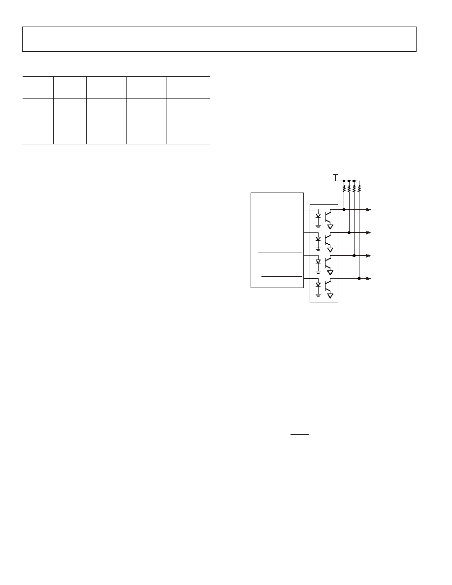
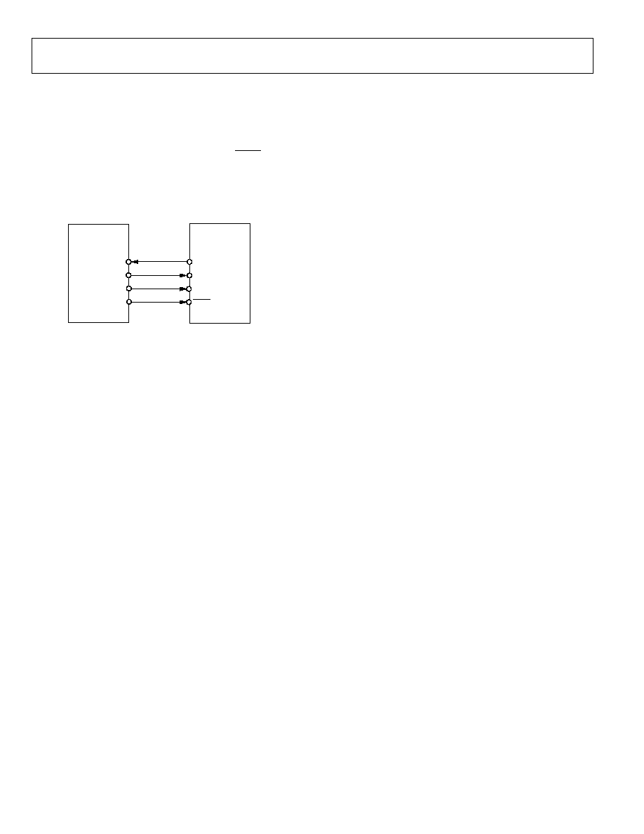
Daisy Chaining
This mode of operation is designed for multi-DAC systems,
where several AD5570s may be connected in cascade as shown
in Figure 37. This is done by connecting the control inputs in
parallel and then daisy chaining the SDIN and SDO I/Os of
each device. An external pull-up resistor of ~5 k on SDO is
required when using the part in daisy-chain mode.
As before, when SYNC goes low, serial data on SDIN is shifted
into the input shift register on the falling edge of SCLK. If more
than 16 clock pulses are applied, the data ripples out of the shift
resister and appears on the SDO line. By connecting this line to
the SDIN input on the next AD5570 in the chain, a multi-DAC
interface may be constructed.
Figure 37. Daisy Chaining Using the AD5570
One data transfer cycle of 16 SCLK pulses is required for each
DAC in the system. Therefore, the total number of clock cycles
must equal 16 N, where N is the total number of devices in the
chain. The first data transfer cycle written into the chain
appears at the last DAC in the system on the final data transfer
cycle.
Readback
The AD5570 allows the data contained in the DAC register to
be read back, if required. As with daisy chaining, an external
pull-up resistor of ~5 k on SDO is required. The data in the
DAC register is available on SDO on the falling edges of SCLK
when SYNC is low. On the sixteenth SCLK edge, SDO is
updated to repeat SDIN with a delay of 16 clock cycles.
When the serial transfer to all devices is complete, SYNC should
be taken high. This prevents any further data from being
clocked into the devices.
To read back the contents of the DAC register without writing
to the part, SYNC should be taken low while LDAC is held high.
A continuous SCLK source may be used, if it can be arranged
that SYNC is held low for the correct number of clock cycles.
Alternatively, a burst clock containing the exact number of
clock cycles may be used and SYNC taken high some time later.
The outputs of all the DACs in the system can be updated
simultaneously using the LDAC signal.
Daisy-chaining readback is also possible through the SDO pin
of the last device in the DAC chain, because the DAC data
passes through the DAC chain with the appropriate latency.

AD5570
Rev. 0 | Page 19 of 24
APPLICATIONS INFORMATION
TYPICAL OPERATING CIRCUIT
Figure 38 shows the typical operating circuit for the AD5570.
The only external component needed for this precision 16-bit
DAC is a single external positive reference. Because the device
incorporates reference buffers, it eliminates the need for a
negative reference, external inverters, precision amplifiers, and
resistors. This leads to an overall saving in both cost and board
space.
In the circuit below, V
DD
and V
SS
are both connected to ±15 V,
but V
DD
and V
SS
can operate supplies from +11.4 V to +16.5 V.
In Figure 38, AGNDS is connected to AGND, but the option of
Force/Sense is included on this device, if required by the user.
1
2
3
4
5
6
7
8
16
15
14
13
12
11
10
9
AD5570
V
SS
V
DD
CLR
LDAC
SYNC
SCLK
SDIN
SDO
REFGND
REFIN
REFGND
V
OUT
AGNDS
AGND
PD
DGND
+15V
0.1
µ
F
10
µ
F
0.1
µ
F
10
µ
F
≠15V
V
OUT
5V
ADR435
03760-
0-
044
LDAC
SYNC
SCLK
SDIN
SDO
5k
Figure 38. Typical Operating Circuit
Force/Sense of AGND
Because of the extremely high accuracy of this device, system
design issues such as grounding and contact resistance are very
important. The AD5570, with ±10 V output, has an LSB size of
305 µV. Therefore, series wiring and connector resistances of
very small values could cause voltage drops of an LSB. For this
reason, the AD5570 offers a Force/Sense output configuration.
Figure 39 shows how to connect the AD5570 to the Force/Sense
amplifier. Where accuracy of the output is important, an ampli-
fier such as the OP177 is ideal. The OP177 is ultraprecise with
offset voltages of 10 µV maximum at room temperature, and
offset drift of 0.1 µV/∞C maximum. Alternative recommended
amplifiers are the OP1177 and the OP77. For applications where
optimization of the circuit for settling time is needed, the
AD845 is recommended.
Precision Voltage Reference Selection
To achieve the optimum performance from the AD5570,
thought should be given to the selection of a precision voltage
reference. The AD5570 has just one reference input, REFIN.
This voltage on REFIN is used to provide a buffered positive
and negative reference for the DAC core. Therefore, any error in
the voltage reference is reflected in the output of the device.
6
2
3
(OTHER CONNECTIONS OMITTED
FOR CLARITY)
OP177*
*FOR OPTIMUM SETTLING TIME PERFORMANCE,
THE AD845 IS RECOMMENDED.
03760-0-045
1
2
3
4
5
6
7
8
16
15
14
13
12
11
10
9
AD5570
V
SS
V
DD
CLR
LDAC
SYNC
SCLK
SDIN
SDO
REFGND
REFIN
REFGND
V
OUT
AGNDS
AGND
PD
DGND
Figure 39. Driving AGND and AGNDS Using a Force/Sense Amplifier
There are four possible sources of error to consider when
choosing a voltage reference for high accuracy applications:
initial accuracy, temperature coefficient of the output voltage,
long term drift, and output voltage noise.
Initial accuracy on the output voltage of an external reference
could lead to a full-scale error in the DAC. Therefore, to
minimize these errors, a reference with low initial accuracy
specification is preferred. Also, choosing a reference with an
output trim adjustment, such as the ADR425, allows a system
designer to trim system errors out by setting the reference
voltage to a voltage other than the nominal. The trim adjust-
ment can also be used at temperature to trim out any error.
Long term drift (LTD) is a measure of how much the reference
drifts over time. A reference with a tight long-term drift
specification ensures that the overall solution remains relatively
stable over its entire lifetime.
The temperature coefficient of a reference's output voltage
affects INL, DNL, and TUE. A reference with a tight tempera-
ture coefficient specification should be chosen to reduce the
dependence of the DAC output voltage on ambient conditions.
In high accuracy applications, which have a relatively low noise
budget, reference output voltage noise needs to be considered.
Choosing a reference with as low an output noise voltage as
practical for the system resolution required is important. Preci-
sion voltage references such as the ADR435 (XFET design)
produce low output noise in the 0.1 Hz to 10 Hz region.
However, as the circuit bandwidth increases, filtering the output
of the reference may be required to minimize the output noise.
AD5570
Rev. 0 | Page 20 of 24
Table 8. Partial List of Precision References Recommended
for Use with the AD5570
Part No.
Initial
Accuracy
(mV max)
Long-Term
Drift
(ppm typ)
Temp Drift
(ppm/
∞C max)
0.1 Hz to
10 Hz Noise
(µV p-p typ)
ADR435
± 6
30 3 3.4
ADR425
± 6
50 3 3.4
ADR02
1
±
5
50 3 15
ADR395
±
6
50 25 5
AD586
±2.5
15 10 4
1
Available in SC70 package.
LAYOUT GUIDELINES
In any circuit where accuracy is important, careful considera-
tion of the power supply and ground return layout helps to
ensure the rated performance. The printed circuit board on
which the AD5570 is mounted should be designed so that the
analog and digital sections are separated and confined to
certain areas of the board. If the AD5570 is in a system where
multiple devices require an AGND-to-DGND connection, the
connection should be made at one point only. The star ground
point should be established as close as possible to the device.
The AD5570 should have ample supply bypassing of 10 µF in
parallel with 0.1 µF on each supply located as close to the pack-
age as possible, ideally right up against the device. The 10 µF
capacitors are the tantalum bead type. The 0.1 µF capacitor
should have low effective series resistance (ESR) and effective
series inductance (ESI) such as the common ceramic types,
which provide a low impedance path to ground at high frequen-
cies to handle transient currents due to internal logic switching.
The power supply lines of the AD5570 should use as large a
trace as possible to provide low impedance paths and reduce the
effects of glitches on the power supply line. Fast switching
signals such as clocks should be shielded with digital ground to
avoid radiating noise to other parts of the board, and should
never be run near the reference inputs. A ground line routed
between the SDIN and SCLK lines helps reduce crosstalk
between them (not required on a multilayer board, which has a
separate ground plane, but separating the lines helps). It is
essential to minimize noise on the REFIN line, because it
couples through to the DAC output.
Avoid crossover of digital and analog signals. Traces on opposite
sides of the board should run at right angles to each other. This
reduces the effects of feed through the board. A microstrip
technique is by far the best, but not always possible with a
double-sided board. In this technique, the component side of
the board is dedicated to ground plane, while signal traces are
placed on the solder side.
OPTO-COUPLER INTERFACE
In many process control applications, it is necessary to provide
an isolation barrier between the controller and the unit being
controlled. Opto-isolators can provide voltage isolation in
excess of 3 kV. The serial loading structure of the AD5570
makes it ideal for opto-isolated interfaces, because the number
of interface lines is kept to a minimum. Figure 40 shows a
4-channel isolated interface to the AD5570. To reduce the
number of opto-isolators, if the simultaneous updating of the
DAC is not required, the LDAC pin may be tied permanently
low. The DAC can then be updated on the rising edge of SYNC.
V
CC
TO SDIN
TO SCLK
TO SYNC
SYNC OUT
SERIAL CLOCK OUT
SERIAL DATA OUT
µ
CONTROLLER
OPTO-COUPLER
TO LDAC
CONTROL OUT
03760-0-050
Figure 40. Opto-Isolated Interface
MICROPROCESSOR INTERFACING
Microprocessor interfacing to the AD5570 is via a serial bus
that uses standard protocol compatible with microcontrollers
and DSP processors. The communications channel is a 3-wire
(minimum) interface consisting of a clock signal, a data signal,
and a synchronization signal. The AD5570 requires a 16-bit
data word with data valid on the falling edge of SCLK.
For all the interfaces, the DAC output update may be done
automatically when all the data is clocked in, or it may be done
under the control of LDAC. The contents of the DAC register
may be read using the readback function.

AD5570
Rev. 0 | Page 21 of 24
AD5570 to MC68HC11 Interface
Figure 41 shows an example of a serial interface between the
AD5570 and the MC68HC11 microcontroller. The serial
peripheral interface (SPI) on the MC68HC11 is configured for
master mode (MSTR = 1), clock polarity bit (CPOL = 0), and
the clock phase bit (CPHA = 1). The SPI is configured by
writing to the SPI control register (SPCR)--see the 68HC11
User Manual. SCK of the 68HC11 drives the SCLK of the
AD5570, the MOSI output drives the serial data line (DIN) of
the AD5570, and the MISO input is driven from SDO. The
SYNC is driven from one of the port lines, in this case PC7.
When data is being transmitted to the AD5570, the SYNC line
(PC7) is taken low and data is transmitted MSB first. Data
appearing on the MOSI output is valid on the falling edge of
SCK. Eight falling clock edges occur in the transmit cycle, so, in
order to load the required 16-bit word, PC7 is not brought high
until the second 8-bit word has been transferred to the DAC's
input shift register.
AD5570*
SCLK
DIN
SYNC
MOSI
SCLK
PC7
MC68HC11*
*ADDITIONAL PINS OMITTED FOR CLARITY
SDO
MISO
03760-0-014
Figure 41. AD5570 to MC68HC11 Interface
LDAC is controlled by the PC6 port output. The DAC can be
updated after each 2-byte transfer by bringing LDAC low. This
example does not show other serial lines for the DAC. If CLR
were used, it could be controlled by port output PC5, for
example.
AD5570 to 8051 Interface
The AD5570 requires a clock synchronized to the serial data.
For this reason, the 8051 must be operated in Mode 0. In this
mode, serial data enters and exits through RxD, and a shift clock
is output on RxD.
P3.3 and P3.4 are bit programmable pins on the serial port and
are used to drive SYNC and LDAC, respectively.
The 8051 provides the LSB of its SBUF register as the first bit in
the data stream. The user must ensure that the data in the SBUF
register is arranged correctly, because the DAC expects MSB
first.
AD5570*
SCLK
DIN
SYNC
TxD
P3.3
8xC51*
*ADDITIONAL PINS OMITTED FOR CLARITY
SDO
RxD
V
LOGIC
LDAC
P3.4
03760-0-015
Figure 42. AD5570 to 8051 Interface
When data is to be transmitted to the DAC, P3.3 is taken low.
Data on RxD is clocked out of the microcontroller on the rising
edge of TxD and is valid on the falling edge. As a result, no glue
logic is required between this DAC and the microcontroller
interface.
The 8051 transmits data in 8-bit bytes with only eight falling
clock edges occurring in the transmit cycle. Because the DAC
expects a 16-bit word, SYNC (P3.3) must be left low after the
first eight bits are transferred. After the second byte has been
transferred, the P3.3 line is taken high. The DAC may be
updated using LDAC via P3.4 of the 8051.
AD5570 to ADSP2101/ADSP2103
An interface between the AD5570 and the ADSP2101/
ADSP2103 is shown in Figure 43. The ADSP2101/ADSP2103
should be set up to operate in the SPORT transmit alternate
framing mode. The ADSP2101/ADSP2103 are programmed
through the SPORT control register and should be configured
as follows: internal clock operation, active low framing, and
16-bit word length.
Transmission is initiated by writing a word to the Tx register
after the SPORT has been enabled. As the data is clocked out of
the DSP on the rising edge of SCLK, no glue logic is required to
interface the DSP to the DAC. In the interface shown, the DAC
output is updated using the LDAC pin via the DSP. Alterna-
tively, the LDAC input could be tied permanently low, and then
the update takes place automatically when TFS is taken high.
AD5570*
SCLK
DIN
SYNC
DT
SCLK
RFS
ADSP2101/
ADSP2103*
*ADDITIONAL PINS OMITTED FOR CLARITY
SDO
DR
TFS
LDAC
FO
03760-0-016
Figure 43. AD5570 to ADSP2101/ADSP2103 Interface
AD5570
Rev. 0 | Page 22 of 24
AD5570 to PIC16C6x/7x
EVALUATION BOARD
The PIC16C6x/7x synchronous serial port (SSP) is configured
as an SPI master with the clock polarity bit set to 0. This is done
by writing to the synchronous serial port control register
(SSPCON). See the PIC16/17 Microcontroller User Manual. In
this example, I/O port RA1 is being used to pulse SYNC and
enable the serial port of the AD5570. This microcontroller
transfers only eight bits of data during each serial transfer
operation; therefore, two consecutive write operations are
needed. Figure 44 shows the connection diagram.
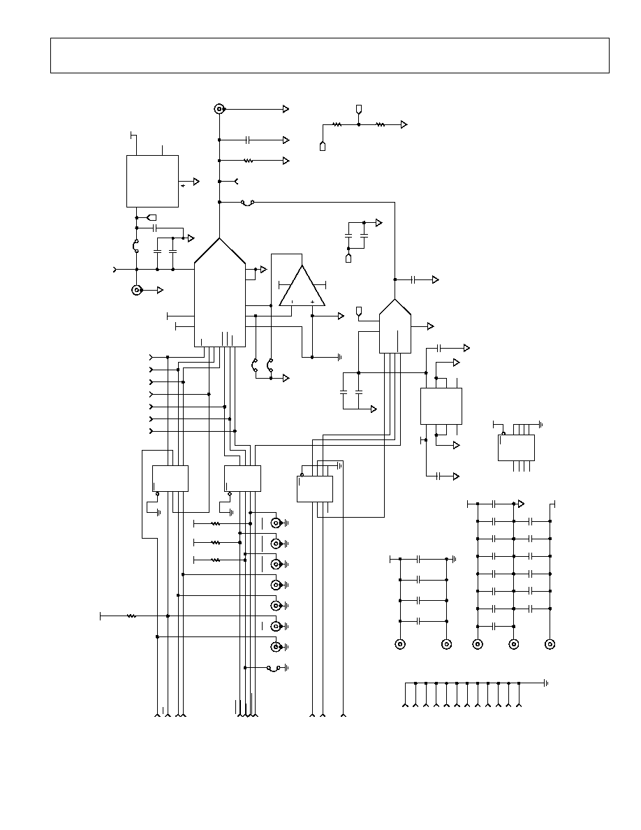
The AD5570 comes with a full evaluation board to aid designers
in evaluating the high performance of the part with a minimum
of effort. All that is required with the evaluation board is a
power supply, a PC, and an oscilloscope.
The AD5570 evaluation kit includes a populated, tested AD5570
printed circuit board. The evaluation board interfaces to the
parallel interface of the PC. Software is available with the
evaluation board, which allows the user to easily program the
AD5570. A schematic of the evaluation board is shown in
Figure 45. The software runs on any PC that has Microsoft
WindowsÆ 95/98/ME/2000 installed.
AD5570*
SCLK
DIN
SYNC
SDO/RC5
SCLK/RC3
RA1
PIC16C6x/7x*
*ADDITIONAL PINS OMITTED FOR CLARITY
SDO
SDI/RC4
03760-0-017
An application note is available that gives full details on
operating the evaluation board.
Figure 44. AD5570 to PIC16C6x/7x Interface
AD5570
Rev. 0 | Page 23 of 24
J11
≠19
J11≠12
J11≠4 J11≠6 J11≠7 J11≠8
J11≠13
J11
≠ CE
NTRONI
CS
CONNE
CTOR
J11≠3
J11≠2 J11≠5
J4
J5
J6
J7
J8
J9
J10
J11≠10
J11≠9
J13
≠1
+
+
+
+
++
+
+
C30
10
µ
F
20V
C12
10
µ
F
C11
10
µ
F
+
C13
10
µ
F
+
C21
10
µ
F
+
C22
10
µ
F
C23
0.
1
µ
F
C24
0.
1
µ
F
C15
0.
1
µ
F
C10
10
µ
F
C9
10
µ
F
C8
0.
1
µ
F
C7
0.
1
µ
F
C6
0.
1
µ
F
C14
0.
1
µ
F
0.
33
µ
F
C2
C4
0.
01
µ
F
C36
0.
1
µ
F
C3
0.
1
µ
F
C35
0.
1
µ
F
C16
0.
1
µ
F
C34
10
µ
F
C5
10
µ
F
R2
10k
R3
10k
C17
0.
1
µ
F
C18
10
µ
F
U5
U3
U1
U2
J1
TP5
VOU
T
C1
R1
RE
F/
2
RE
F/
2
OP
V+
V
≠
WHI
T
E
P
L
AS
TI
C S
S
OP
CLAM
P
O
P
177
ADR435
AD5570
C31
0.
1
µ
F
C32
0.
1
µ
F
C33
0.
1
µ
F
DGND
DGND
DV
DD
DV
DD
J13
≠2
J12
≠1
J12
≠2
J11
≠20
J11
≠21
J11
≠22
J11
≠23
J11
≠24
J11
≠25
J11
≠26
J11
≠27
J11
≠28
J11
≠29
J11
≠30
AV
DD
AV
DD
AV
DD
VSS
AV
DD
DV
DD
AV
DD
LK2
LK1
TP4
TP10
TP7
TP1
TP2
TP9
TP3
TP8
J2
LK3
VSS
AGND
DGND
AV
DD
AV
DD
Y0
VIN
SCL
K
PD SDO DIN SCL
K
SYNC LDAC CLR
VDD
VDD
REFIN
VSS
REFIN
LK5
GND
DGN
D
AGNDS
AGND
REFGND
REFGND
SDATA BUSY
G
ND4
U6
G
ND3
VOUT
VIN
VOUT
VOUT
+
V
IN
TRIM
GN
D
G
ND2
G
ND1
9
8
7
6
5
1
2
3
3
2
2
91
2
12
1
5
62
5
11
16
14
13
3
7
6
4
1
8
4
5 6 7
10 8 7 6 5 4 3
4
7 5 3
11
19
13 15 17
Y1 Y2 Y3
A0 A1 A2 A3
AGND
VSS
74ACT244
LM78L05ACM
AD7895-10
U4≠B
AGND
J12
≠3
VSS
OE
Y0
18 16 14 12
2
1
4 6 8
Y1 Y2 Y3
A0 A1 A2 A3
74ACT244
U4≠
A
OE
2
1
4 6 8
18 16 14 12
Y0 Y1 Y2 Y3
A0 A1 A2 A3
74ACT244
U9≠A
OE
11
19
13 15 17
9 7 5 3
Y0 Y1 Y2 Y3
A0 A1 A2 A3
74ACT244
U9≠B
SD
O
D
IN
SC
LK
SCLK_ADC
SDATA_ADC
DATA
SCL
K
DIN
DO
UT
OE
RE
F/
2
RE
F
REF
CO
NVST
CLR
PD
CO
NVST
LDAC
SYNC
R4
4k7
DV
DD
R5
4k7
R7
4k7
R6
4k7
DV
DD
DV
DD
LK4
PD
LDAC
SYN
C
CLR
03760-0-043
Figure 45. Evaluation Board Schematic

AD5570
Rev. 0 | Page 24 of 24
OUTLINE DIMENSIONS
16
9
8
1
6.50
6.20
5.90
8.20
7.80
7.40
SEATING
PLANE
0.05 MIN
0.65
BSC
2.00 MAX
0.25
0.09
0.95
0.75
0.55
0.38
0.22
5.60
5.30
5.00
COPLANARITY
0.10
8∞
4∞
0∞
1.85
1.75
1.65
COMPLIANT TO JEDEC STANDARDS MO-150AC
Figure 46. 16-Lead Shrink Small Outline Package [SSOP]
(RS-16)
Dimensions shown in millimeters
ORDERING GUIDE
Model
Temperature Range
Package Description
Package Option
AD5570ARS
-40 ∞C to +85 ∞C
16-Lead SSOP
RS-16
AD5570ARS-REEL
-40 ∞C to +85 ∞C
16-Lead SSOP
RS-16
AD5570ARS-REEL7
-40 ∞C to +85 ∞C
16-Lead SSOP
RS-16
AD5570BRS
-40 ∞C to +85 ∞C
16-Lead SSOP
RS-16
AD5570BRS-REEL
-40 ∞C to +85 ∞C
16-Lead SSOP
RS-16
AD5570BRS-REEL7
-40 ∞C to +85 ∞C
16-Lead SSOP
RS-16
AD5570WRS
-40 ∞C to +125 ∞C
16-Lead SSOP
RS-16
AD5570WRS-REEL
-40 ∞C to +125 ∞C
16-Lead SSOP
RS-16
AD5570WRS-REEL7
-40 ∞C to +125 ∞C
16-Lead SSOP
RS-16
AD5570YRS
-40 ∞C to +125 ∞C
16-Lead SSOP
RS-16
AD5570YRS-REEL
-40 ∞C to +125 ∞C
16-Lead SSOP
RS-16
AD5570YRS-REEL7
-40 ∞C to +125 ∞C
16-Lead SSOP
RS-16
Eval-AD5570EB
Evaluation
Board
© 2003 Analog Devices, Inc. All rights reserved. Trademarks and
registered trademarks are the property of their respective owners.
C03760≠0≠11/03(0)