 | ÐлекÑÑоннÑй компоненÑ: AD557JP | СкаÑаÑÑ:  PDF PDF  ZIP ZIP |
Äîêóìåíòàöèÿ è îïèñàíèÿ www.docs.chipfind.ru
REV. A
Information furnished by Analog Devices is believed to be accurate and
reliable. However, no responsibility is assumed by Analog Devices for its
use, nor for any infringements of patents or other rights of third parties
which may result from its use. No license is granted by implication or
otherwise under any patent or patent rights of Analog Devices.
a
DACPORT, Low-Cost Complete
P-Compatible 8-Bit DAC
AD557
FEATURES
Complete 8-Bit DAC
Voltage Output--0 V to 2.56 V
Internal Precision Band-Gap Reference
Single-Supply Operation: +5 V ( 10%)
Full Microprocessor Interface
Fast: 1 s Voltage Settling to 1/2 LSB
Low Power: 75 mW
No User Trims Required
Guaranteed Monotonic Over Temperature
All Errors Specified T
MIN
to T
MAX
Small 16-Pin DIP or 20-Pin PLCC Package
Low Cost
GENERAL DESCRIPTION
The AD557 DACPORT® is a complete voltage-output 8-bit
digital-to-analog converter, including output amplifier, full
microprocessor interface and precision voltage reference on a
single monolithic chip. No external components or trims are
required to interface, with full accuracy, an 8-bit data bus to an
analog system.
The low cost and versatility of the AD557 DACPORT are the re-
sult of continued development in monolithic bipolar technologies.
The complete microprocessor interface and control logic is
implemented with integrated injection logic (I
2
L), an extremely
dense and low-power logic structure that is process-compatible
with linear bipolar fabrication. The internal precision voltage
reference is the patented low-voltage band-gap circuit which
permits full-accuracy performance on a single +5 V power sup-
ply. Thin-film silicon-chromium resistors provide the stability
required for guaranteed monotonic operation over the entire
operating temperature range, while laser-wafer trimming of
these thin-film resistors permits absolute calibration at the fac-
tory to within
±
2.5 LSB; thus, no user-trims for gain or offset
are required. A new circuit design provides voltage settling to
±
1/2 LSB for a full-scale step in 800 ns.
The AD557 is available in two package configurations. The
AD557JN is packaged in a 16-pin plastic, 0.3"-wide DIP. For
surface mount applications, the AD557JP is packaged in a
20-pin JEDEC standard PLCC. Both versions are specified over
the operating temperature range of 0
°
C to +70
°
C.
DACPORT is a registered trademark of Analog Devices, Inc.
Covered by U.S. Patent Nos. 3,887,863; 3,685,045; 4,323,795; other
patents pending.
One Technology Way, P.O. Box 9106, Norwood, MA 02062-9106, U.S.A.
Tel: 617/329-4700
Fax: 617/326-8703
PRODUCT HIGHLIGHTS
1. The 8-bit I
2
L input register and fully microprocessor-
compatible control logic allow the AD557 to be directly con-
nected to 8- or 16-bit data buses and operated with standard
control signals. The latch may be disabled for direct DAC
interfacing.
2. The laser-trimmed on-chip SiCr thin-film resistors are cali-
brated for absolute accuracy and linearity at the factory.
Therefore, no user trims are necessary for full rated accuracy
over the operating temperature range.
3. The inclusion of a precision low-voltage band-gap reference
eliminates the need to specify and apply a separate reference
source.
4. The AD557 is designed and specified to operate from a single
+4.5 V to +5.5 V power supply.
5. Low digital input currents, 100
µ
A max, minimize bus loading.
Input thresholds are TTL/low voltage CMOS compatible.
6. The single-chip, low power I
2
L design of the AD557 is inher-
ently more reliable than hybrid multichip or conventional
single-chip bipolar designs.
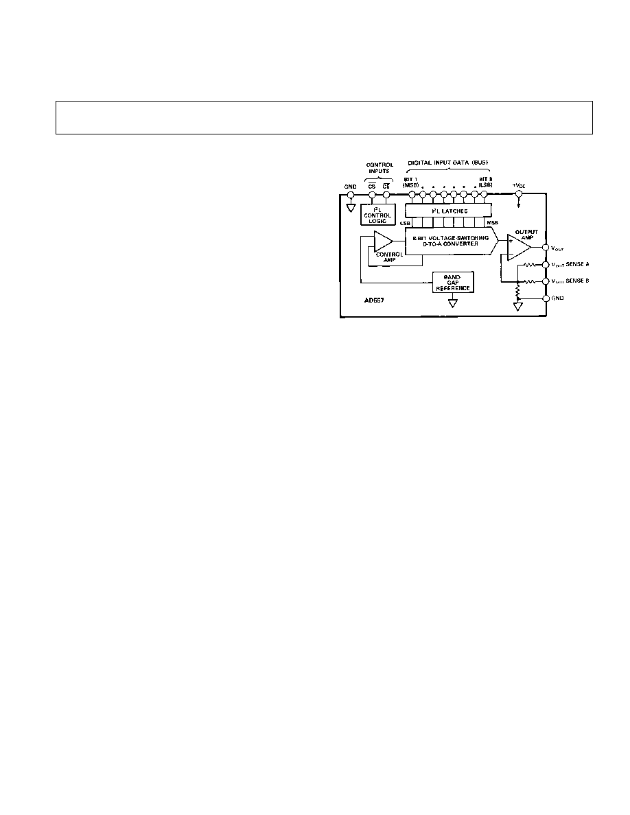
FUNCTIONAL BLOCK DIAGRAM
AD557SPECIFICATIONS
Model
Min
Typ
Max
Units
RESOLUTION
8
Bits
RELATIVE ACCURACY
0 to + 70
°
C
±
1/2
1
LSB
OUTPUT
Ranges
0 to + 2.56
V
Current Source
+5
mA
Sink
Internal Passive
Pull-Down to Ground
2
OUTPUT SETTLING TIME
3
0.8
1.5
µ
s
FULL-SCALE ACCURACY
4
@ +25
°
C
±
1.5
±
2.5
LSB
T
MIN
to T
MAX
±
2.5
±
4.0
LSB
ZERO ERROR
@ +25
°
C
±
1
LSB
T
MIN
to T
MAX
±
3
LSB
MONOTONICITY
5
T
MIN
to T
MAX
Guaranteed
DIGITAL INPUTS
T
MIN
to T
MAX
Input Current
100
µ
A
Data Inputs, Voltage
Bit On--Logic "1"
2.0
V
Bit On--Logic "0"
0
0.8
V
Control Inputs, Voltage
On--Logic "1"
2.0
V
On--Logic "0"
0
0.8
V
Input Capacitance
4
pF
TIMING
6
t
W
Strobe Pulse Width
225
ns
T
MIN
to T
MAX
300
ns
t
DH
Data Hold Time
10
ns
T
MIN
to T
MAX
10
ns
t
DS
Data Setup Time
225
ns
T
MIN
to T
MAX
300
ns
POWER SUPPLY
Operating Voltage Range (V
CC
)
2.56 Volt Range
+4.5
+5.5
V
Current (I
CC
)
15
25
mA
Rejection Ratio
0.03
%/%
POWER DISSIPATION, V
CC
= 5 V
75
125
mW
OPERATING TEMPERATURE RANGE
0
+70
°
C
NOTES
1
Relative Accuracy is defined as the deviation of the code transition points from the
ideal transfer point on a straight line from the zero the the full scale of the device.
2
Passive pull-down resistance is 2 k
.
3
Settling time is specified for a positive-going full-scale step to
±
1/2 LSB. Negative-
going steps to zero are slower, but can be improved with an external pull-down.
4
The full-scale output voltage is 2.55 V and is guaranteed with a +5 V supply.
5
A monotonic converter has a maximum differential lineraity error of
±
1 LSB.
6
See Figure 7.
Specifications subject to change without notice.
(@ T
A
= +25 C, V
CC
= +5 V unless otherwise noted)
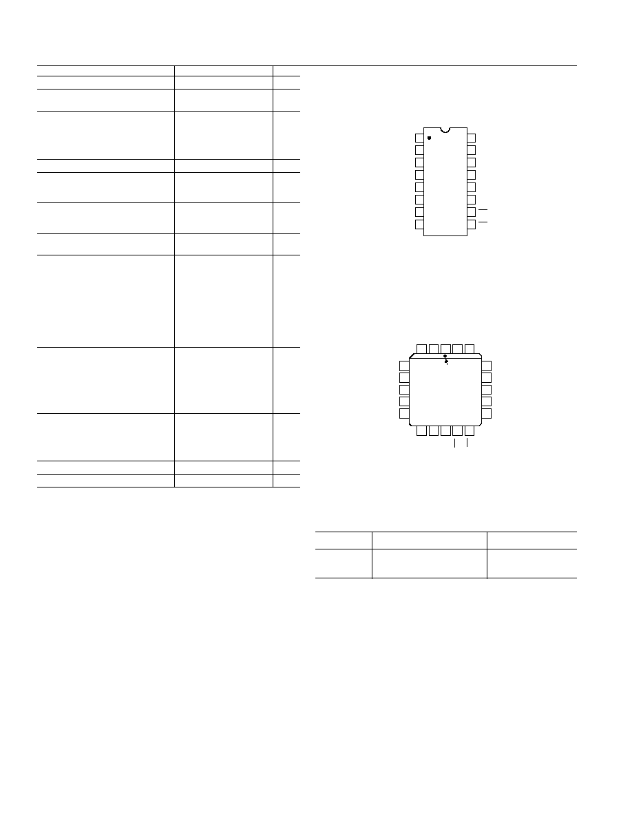
PIN CONFIGURATIONS
DIP
10
9
13
12
11
16
15
14
8
1
2
3
4
7
6
5
TOP VIEW
(Not to Scale)
AD557
LSB BIT 8
GND
V
OUT
SENSE B
V
OUT
SENSE A
V
OUT
BIT 7
BIT 6
BIT 5
CS
+V
CC
GND
BIT 4
BIT 3
BIT 2
MSB BIT 1
CE
PLCC
NC
20 19
18
1
2
3
4
5
6
7
8
9
10
11 12
13
14
15
16
17
TOP VIEW
(Not to Scale)
PIN 1
IDENTIFIER
BIT 6
BIT 5
NC
BIT 4
BIT 3
V
OUT
SENSE B
GND
NC
GND
+V
CC
NC = NO CONNECT
AD557
BIT 7
BIT 8 (LSB)
NC
V
OUT
V
OUT
SENSE A
BIT 2
(MSB) BIT 1
CE
CS
ABSOLUTE MAXIMUM RATINGS
*
V
CC
to Ground . . . . . . . . . . . . . . . . . . . . . . . . . . . 0 V to +18 V
Digital Inputs (Pins 110) . . . . . . . . . . . . . . . . . . 0 V to +7.0 V
V
OUT
. . . . . . . . . . . . . . . . . . . . . . . Indefinite Short to Ground
Momentary Short to V
CC
Power Dissipation . . . . . . . . . . . . . . . . . . . . . . . . . . . . 450 mW
Storage Temperature Range
N/P (Plastic) Packages . . . . . . . . . . . . . . . . 25
°
C to +100
°
C
Lead Temperature (Soldering, 10 sec) . . . . . . . . . . . . . . 300
°
C
Thermal Resistance
Junction to Ambient/Junction to Case
N/P (Plastic) Packages . . . . . . . . . . . . . . . . . . 140/55
°
C/W
*Stresses above those listed under "Absolute Maximum Ratings" may cause
permanent damage to the device. This is a stress rating only and functional
operation of the device at these or any other conditions above those indicated
in the operational section of this specification is not implied. Exposure to absolute
maximum rating conditions for extended periods may affect device reliability.
REV. A
2
ORDERING GUIDE
Model
Temperature Range
Package Option*
AD557JN
0
°
C to +70
°
C
N-16
AD557JP
0
°
C to +70
°
C
P-20A
*N = Plastic DIP; P = Plastic Leaded Chip Carrier.
CIRCUIT DESCRIPTION
The AD557 consists of four major functional blocks fabricated
on a single monolithic chip (see Figure 1). The main D/A con-
verter section uses eight equally weighted laser-trimmed current
sources switched into a silicon-chromium thin-film R/2R resistor
ladder network to give a direct but unbuffered 0 mV to 400 mV
output range. The transistors that form the DAC switches are
PNPs; this allows direct positive-voltage logic interface and a
zero-based output range.
AD557
REV.A
3
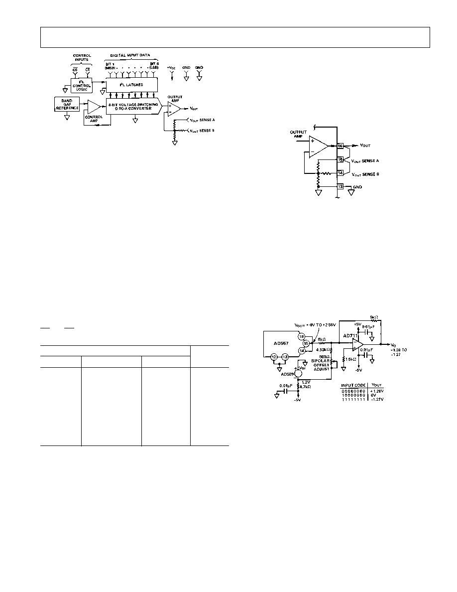
Figure 1. Functional Block Diagram
The high-speed output buffer amplifier is operated in the
noninverting mode with gain determined by the user-
connections at the output range select pin. The gain-setting
application resistors are thin film laser trimmed to match and
track the DAC resistors and to assure precise initial calibration
of the output range, 0 V to 2.56 V. The amplifier output stage is
an NPN transistor with passive pull-down for zero-based output
capability with a single power supply.
The internal precision voltage reference is of the patented
band-gap type. This design produces a reference voltage of
1.2 V and thus, unlike 6.3 V temperature-compensated Zeners,
may be operated from a single, low-voltage logic power supply.
The microprocessor interface logic consists of an 8-bit data latch
and control circuitry. Low power, small geometry and high
speed are advantages of the I
2
L design as applied to this section.
I
2
L is bipolar process compatible so that the performance of the
analog sections need not be compromised to provide on-chip
logic capabilities. The control logic allows the latches to be
operated from a decoded microprocessor address and write sig-
nal. If the application does not involve a
µ
P or data bus, wiring
CS
and CE to ground renders the latches "transparent" for
direct DAC access.
Digital Input Code
Output
Binary
Hexadecimal
Decimal
Voltage
0000 0000
00
0
0
0000 0001
01
1
0.010 V
0000 0010
02
2
0.020 V
0000 1111
0F
15
0.150 V
0001 0000
10
16
0.160 V
0111 1111
7F
127
1.270 V
1000 0000
80
128
1.280 V
1100 0000
C0
192
1.920 V
1111 1111
FF
255
2.55 V
CONNECTING THE AD557
The AD557 has been configured for low cost and ease of appli-
cation. All reference, output amplifier and logic connections are
made internally. In addition, all calibration trims are performed
at the factory assuring specified accuracy without user trims.
The only connection decision to be made by the user is whether
the output range desired is unipolar or bipolar. Clean circuit
board layout is facilitated by isolating all digital bit inputs on
one side of the package; analog outputs are on the opposite side.
UNIPOLAR 0 V TO +2.56 V OUTPUT RANGE
Figure 2 shows the configuration for the 0 V to +2.56 V full-
scale output range. Because of its precise factory calibration, the
AD557 is intended to be operated without user trims for gain
and offset; therefore, no provisions have been made for such
user trims. If a small increase in scale is required, however, it
may be accomplished by slightly altering the effective gain of the
output buffer. A resistor in series with V
OUT
SENSE will
increase the output range. Note that decreasing the scale by put-
ting a resistor in series with GND will not work properly due to
the code-dependent currents in GND. Adjusting offset by
injecting dc at GND is not recommended for the same reason.
Figure 2. 0 V to 2.56 V Output Range
BIPOLAR 1.28 V TO +1.28 V OUTPUT RANGE
The AD557 was designed for operation from a single power
supply and is thus capable of providing only a unipolar 0 V to
+2.56 V output range. If a negative supply is available, bipolar
output ranges may be achieved by suitable output offsetting and
scaling. Figure 3 shows how a
±
1.28 V output range may be
achieved when a 5 V power supply is available. The offset is
provided by the AD589 precision 1.2 V reference which will
operate from a +5 V supply. The AD711 output amplifier can
provide the necessary
±
1.28 V output swing from
±
5 V supplies.
Coding is complementary offset binary.
Figure 3. Bipolar Operation of AD557 from
±
5 V Supplies
Applications
GROUNDING AND BYPASSING
All precision converter products require careful application of
good grounding practices to maintain full rated performance.
Because the AD557 is intended for application in microcom-
puter systems where digital noise is prevalent, special care must
be taken to assure that its inherent precision is realized.
The AD557 has two ground (common) pins; this minimizes
ground drops and noise in the analog signal path. Figure 4
shows how the ground connections should be made.
It is often advisable to maintain separate analog and digital
grounds throughout a complete system, tying them common in
one place only. If the common tie-point is remote and accidental
disconnection of that one common tie-point occurs due to card
removal with power on, a large differential voltage between the
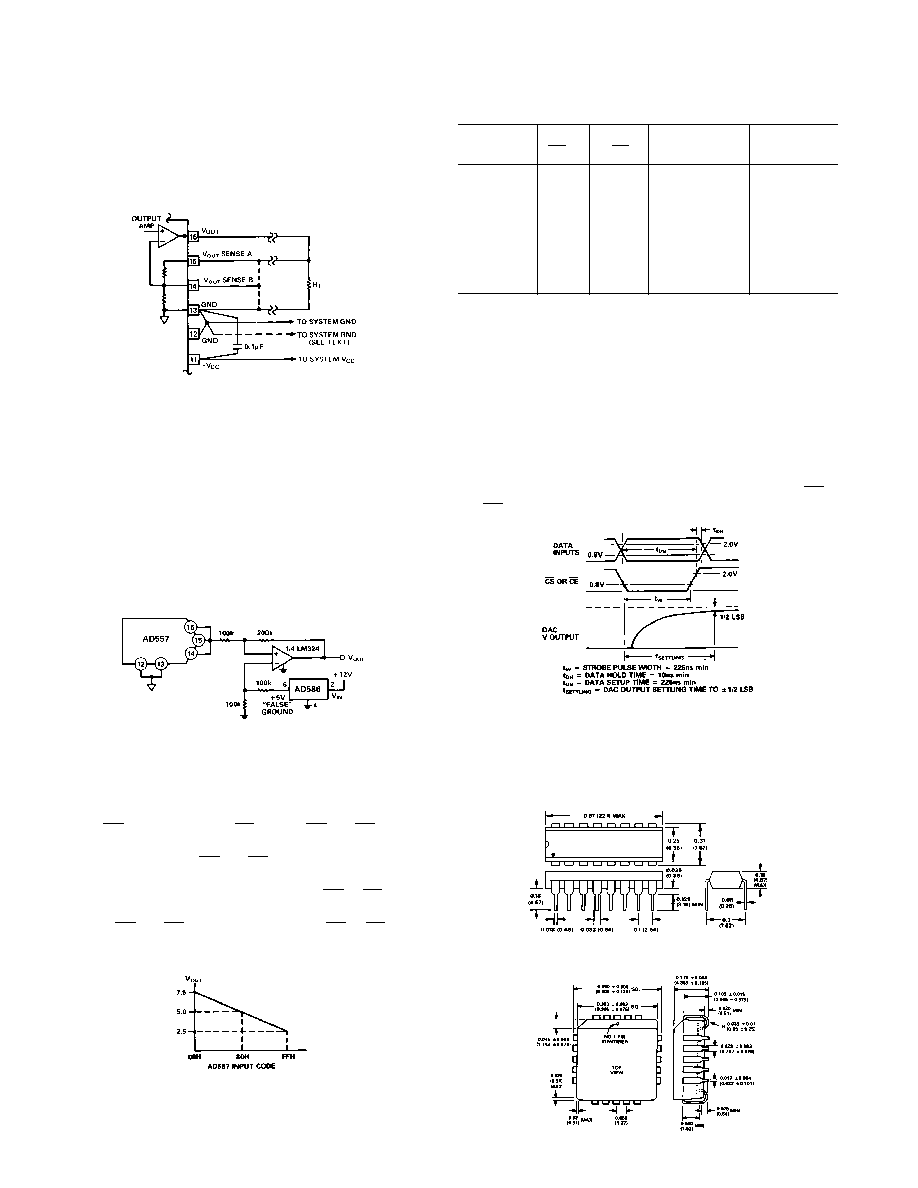
AD557
REV. A
4
PRINTED IN U.S.A.
two commons could develop. To protect devices that interface
to both digital and analog parts of the system, such as the
AD557, it is recommended that common ground tie-points
should be provided at each such device. If only one system
ground can be connected directly to the AD557, it is recom-
mended that analog common be selected.
Figure 4. Recommended Grounding and Bypassing
USING A "FALSE" GROUND
Many applications, such as disk drives, require servo control
voltages that swing on either side of a "false" ground. This
ground is usually created by dividing the +12 V supply equally
and calling the midpoint voltage "ground."
Figure 5 shows an easy and inexpensive way to implement this.
The AD586 is used to provide a stable 5 V reference from the
system's +12 V supply. The op amp shown likewise operates
from a single (+12 V) supply available in the system. The result-
ing output at the V
OUT
node is
±
2.5 V around the "false"
ground point of 5 V. AD557 input code vs. V
OUT
is shown in
Figure 6.
Figure 5. Level Shifting the AD557 Output Around a
"False" Ground
TIMING AND CONTROL
The AD557 has data input latches that simplify interface to 8-
and 16-bit data buses. These latches are controlled by Chip
Enable (CE) and Chip Select (CS) inputs. CE and CS are inter-
nally "NORed" so that the latches transmit input data to the
DAC section when both CE and CS are at Logic "0". If the
application does not involve a data bus, a "00" condition allows
for direct operation of the DAC. When either CE or CS go to
Logic "1," the input data is latched into the registers and held
until both CE and CS return to "0." (Unused CE or CS inputs
should be tied to ground.) The truth table is given in Table I.
The logic function is also shown in Figure 6.
Figure 6. AD557 Input Code vs. Level Shifted Output in a
"False" Ground Configuration
Table I. AD557 Control Logic Truth Table
Latch
Input Data
CE
CS
DAC Data
Condition
0
0
0
0
"transparent"
1
0
0
1
"transparent"
0
g
0
0
latching
1
g
0
1
latching
0
0
g
0
latching
1
0
g
1
latching
X
1
X
previous data
latched
X
X
1
previous data
latched
NOTES
X = Does not matter
g
= Logic Threshold at Positive-Going Transition
In a level-triggered latch such as that used in the AD557, there
is an interaction between the data setup and hold times and the
width of the enable pulse. In an effort to reduce the time
required to test all possible combinations in production, the
AD557 is tested with T
DS
= T
W
= 225 ns at 25
°
C and 300 ns at
T
MIN
and T
MAX
, with T
DH
= 10 ns at all temperatures. Failure
to comply with these specifications may result in data not being
latched properly.
Figure 7 shows the timing for the data and control signals, CE
and CS are identical in timing as well as in function.
Figure 7. AD557 Timing
OUTLINE DIMENSIONS
Dimensions shown in inches and (mm).
N (Plastic) Package
P (PLCC) Package
C1109a56/88