 | ÐлекÑÑоннÑй компоненÑ: AD5611 | СкаÑаÑÑ:  PDF PDF  ZIP ZIP |
Äîêóìåíòàöèÿ è îïèñàíèÿ www.docs.chipfind.ru
2.7 V to 5.5 V, <100 µA, 8-/10-/12-Bit
nanoDACTM D/A, SPI
®
Interface, SC70 Package
Preliminary Technical Data
AD5601/AD5611/AD5621
Rev. PrC
Information furnished by Analog Devices is believed to be accurate and reliable.
However, no responsibility is assumed by Analog Devices for its use, nor for any
infringements of patents or other rights of third parties that may result from its use.
Specifications subject to change without notice. No license is granted by implication
or otherwise under any patent or patent rights of Analog Devices. Trademarks and
registered trademarks are the property of their respective owners.
One Technology Way, P.O. Box 9106, Norwood, MA 02062-9106, U.S.A.
Tel: 781.329.4700
www.analog.com
Fax: 781.326.8703
© 2004 Analog Devices, Inc. All rights reserved.
FEATURES
6-lead SC70 package
Power-down to <100 nA @ 3 V
Micropower operation: max 100 µA @ 5 V
2.7 V to 5.5 V power supply
Guaranteed monotonic by design
Power-on reset to 0 V with brownout detection
3 power-down functions
Low power serial interface with Schmitt-triggered inputs
On-chip output buffer amplifier, rail-to-rail operation
SYNC interrupt facility
Minimized zero code error
AD5601 buffered 8-bit DAC in SC70:
B Version: ±0.5 LSB INL
AD5611 buffered 10-bit DAC in SC70:
B Version: ±0.5 LSB INL
A Version: ±4 LSB INL
AD5621 buffered 12-bit DAC in SC70:
B Version: ±1 LSB INL
A Version: ±6 LSB INL
APPLICATIONS
Voltage level setting
Portable battery-powered instruments
Digital gain and offset adjustment
Programmable voltage and current sources
Programmable attenuators
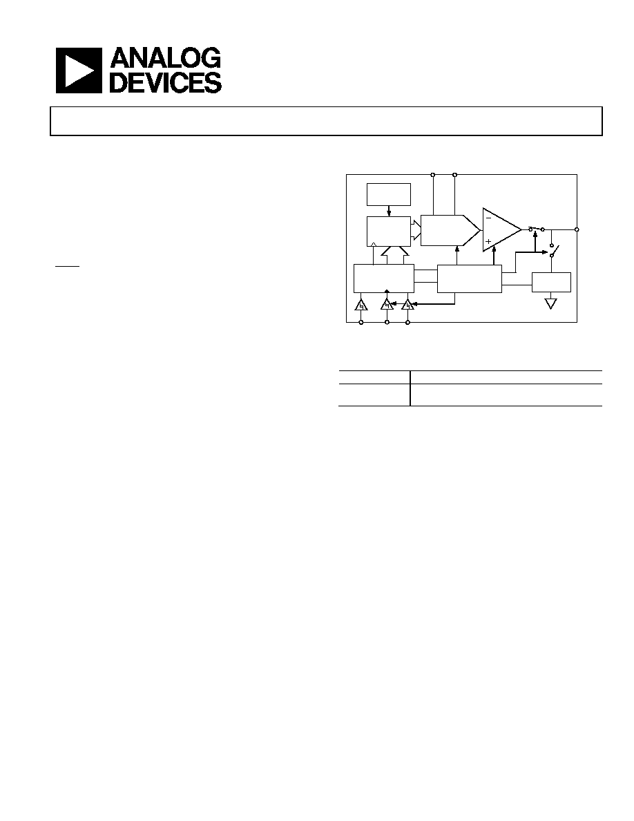
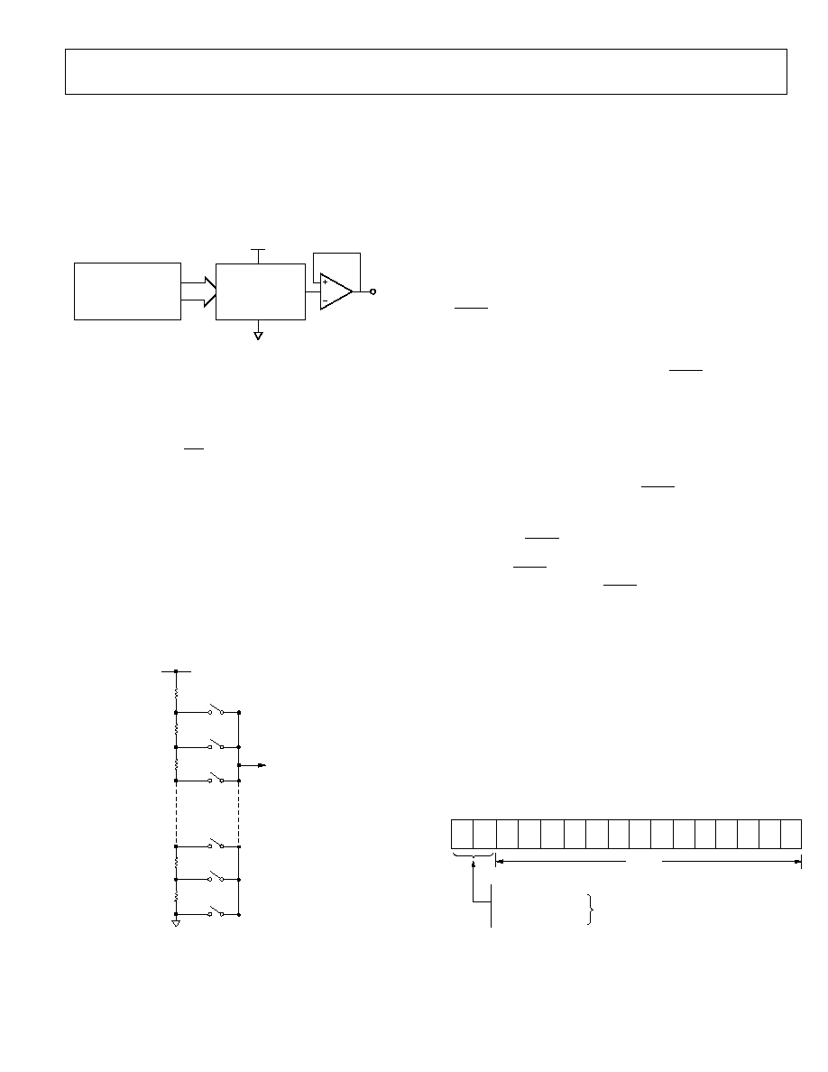
FUNCTIONAL BLOCK DIAGRAM
POWER-ON
RESET
DAC
REGISTER
14-BIT
DAC
INPUT
CONTROL
LOGIC
POWER-DOWN
CONTROL LOGIC
AD5601/AD5611/AD5621
V
DD
GND
REF(+)
RESISTOR
NETWORK
V
OUT
SYNC
SCLK
DIN
OUTPUT
BUFFER
04783-4-001
Figure 1.
Table 1. Related Devices
Part Number
Description
AD5641
2.7 V to 5.5 V, <100 µA, 14-Bit, nanoDAC D/A, tiny
SC70 Package
GENERAL DESCRIPTION
The AD5601/AD5611/AD5621, members of the nanoDAC
family, are single, 8-/10-/12-bit, buffered, voltage out DACs that
operate from a single 2.7 V to 5.5 V supply, consuming <100 µA
at 5 V. The parts come in a tiny SC70 package. Their on-chip
precision output amplifier allows rail-to-rail output swing to be
achieved. The AD5601/AD5611/AD5621 utilize a versatile
3-wire serial interface that operates at clock rates up to 30 MHz
and is compatible with SPI®, QSPITM, MICROWIRETM, and DSP
interface standards.
The reference for the AD5601/AD5611/AD5621 is derived from
the power supply inputs and, therefore, gives the widest
dynamic output range. The parts incorporate a power-on reset
circuit, which ensures that the DAC output powers up to 0 V
and remains there until a valid write to the device takes place.
The AD5601/AD5611/AD5621 contain a power-down feature
that reduces current consumption to <100 nA at 3 V, and
provides software-selectable output loads while in power-down
mode. The parts are put into power-down mode over the serial
interface. The low power consumption of these parts in normal
operation makes them ideally suited to portable battery-
operated equipment. The combination of small package and low
power makes these nanoDAC devices ideal for level-setting
requirements such as generating bias or control voltages in
space-constrained and power-sensitive applications.
(continued on Page 3)

AD5601/AD5611/AD5621
Preliminary Technical Data
Rev. PrC | Page 2 of 20
TABLE OF CONTENTS
Product Highlights ........................................................................... 3
Specifications..................................................................................... 4
Timing Characteristics ................................................................ 5
Absolute Maximum Ratings............................................................ 6
ESD Caution.................................................................................. 6
Pin Configuration and Function DescriptionS ............................ 7
Terminology ...................................................................................... 8
Typical Performance Characteristics ............................................. 9
General Description ....................................................................... 13
D/A Section................................................................................. 13
Resistor String ............................................................................. 13
Output Amplifier ........................................................................ 13
Serial Interface ............................................................................ 13
Input Shift Register .................................................................... 13
SYNC Interrupt .......................................................................... 14
Power-On Reset.......................................................................... 14
Power-Down Modes .................................................................. 14
Microprocessor Interfacing....................................................... 14
Applications..................................................................................... 16
Choosing a Reference as Power Supply for
AD5601/AD5611/AD5621 ....................................................... 16
Bipolar Operation Using the AD5601/ AD5611/AD5621 .... 16
Using AD5601/AD5611/AD5621 with an Opto-Isolated
Interface ....................................................................................... 17
Power Supply Bypassing and Grounding................................ 17
Outline Dimensions ....................................................................... 18
Ordering Guide .......................................................................... 18
REVISION HISTORY
Revision PrC: Preliminary Version

Preliminary Technical Data
AD5601/AD5611/AD5621
Rev. PrC | Page 3 of 20
PRODUCT HIGHLIGHTS
1.
Available in a space-saving 6-lead SC70 package.
2.
Low power, single-supply operation. The AD5601/
AD5611/AD5621 operate from a single 2.7 V to 5.5 V
supply and typically consume 0.2 mW at 3 V and 0.5 mW
at 5 V, making them ideal for battery-powered applications.
3.
The on-chip output buffer amplifier allows the output of
the DAC to swing rail-to-rail with a typical slew rate of
0.5 V/µs.
4.
Reference derived from the power supply.
5.
High speed serial interface with clock speeds up to
30 MHz.
6.
Designed for very low power consumption. The interface
powers up only during a write cycle.
7.
Power-down capability. When powered down, the DAC
typically consumes <100 nA at 3 V.

AD5601/AD5611/AD5621
Preliminary Technical Data
Rev. PrC | Page 4 of 20
SPECIFICATIONS
V
DD
= 2.7 V to 5.5 V; R
L
= 2 k to GND; C
L
= 200 pF to GND; all specifications T
MIN
to T
MAX
, unless otherwise noted.
Table 2.
B
Version
1
Parameter Min
Typ
Max
Unit
Test
Conditions/Comments
STATIC PERFORMANCE
AD5601
Resolution 8
Bits
Relative Accuracy
2
±0.5
LSB
B
Grade
Differential Nonlinearity
2
±1
LSB
Guaranteed monotonic by design
AD5611
Resolution 10
Bits
Relative Accuracy
2
±0.5
LSB
B
Grade
±4.0
LSB
A
Grade
Differential Nonlinearity
2
±1
LSB
Guaranteed monotonic by design
AD5621
Resolution 12
Bits
Relative Accuracy
2
±1
LSB
B
Grade
±6
LSB
A
Grade
Differential Nonlinearity
2
±1
LSB
Guaranteed monotonic by design
Zero Code Error
±0.2
mV
All 0s loaded to DAC register
Offset Error
±0.125
% of FSR
Full-Scale Error
±0.01
LSB
All 1s loaded to DAC register
Gain Error
±0.04
% of FSR
Zero Code Error Drift
5.0
µV/°C
Gain Temperature Coefficient
2.0
ppm of FSR/°C
OUTPUT CHARACTERISTICS
3
Output Voltage Range
0
V
DD
V
Output Voltage Settling Time
8
18
µs
Code ¼ to ¾
Slew Rate
0.5
V/µs
Capacitive Load Stability
470
pF
R
L
=
1000
pF
RL = 2 k
Output Noise Spectral Density
120
nV/Hz
DAC code = TBD, 10 kHz
Noise
TBD
DAC code = TBD, 0.1 Hz to 10 Hz bandwidth
Digital-to-Analog Glitch Impulse
10
nV-s
1 LSB change around major carry
Digital Feedthrough
0.5
nV-s
DC Output Impedance
1
Short-Circuit Current
20
mA
V
DD
= ±3 V/±5 V
LOGIC INPUTS
Input Current
±1
µA
V
INL
, Input Low Voltage
0.8
V
V
DD
= ±5 V
0.6
V
V
DD
= ±2.7 V
V
INH
, Input High Voltage
1.8
V
V
DD
= ±5 V
1.4
V
V
DD
= ±2.7 V
Pin Capacitance
3
pF
Preliminary Technical Data
AD5601/AD5611/AD5621
Rev. PrC | Page 5 of 20
B
Version
1
Parameter Min
Typ
Max
Unit
Test
Conditions/Comments
POWER REQUIREMENTS
V
DD
2.7
5.5
V
All digital inputs at 0 or V
DD
I
DD
(Normal Mode)
DAC active and excluding load current
V
DD
= ±4.5 V to ±5.5 V
100
µA
V
IH
= V
DD
and V
IL
= GND
V
DD
= ±2.7 V to ±3.6 V
70
µA
V
IH
= V
DD
and V
IL
= GND
I
DD
(All Power-Down Modes)
V
DD
= ±4.5 V to ±5.5 V
0.2
1
µA
V
IH
= V
DD
and V
IL
= GND
V
DD
= ±2.7 V to ±3.6 V
0.05
1
µA
V
IH
= V
DD
and V
IL
= GND
POWER EFFICIENCY
I
OUT
/I
DD
TBD %
I
LOAD
= 2 mA and V
DD
= ±5 V
1
Temperature ranges are as follows: B Version: 40°C to +125°C, typical at +25°C.
2
Linearity calculated using a reduced code range.
3
Guaranteed by design and characterization, not production tested.
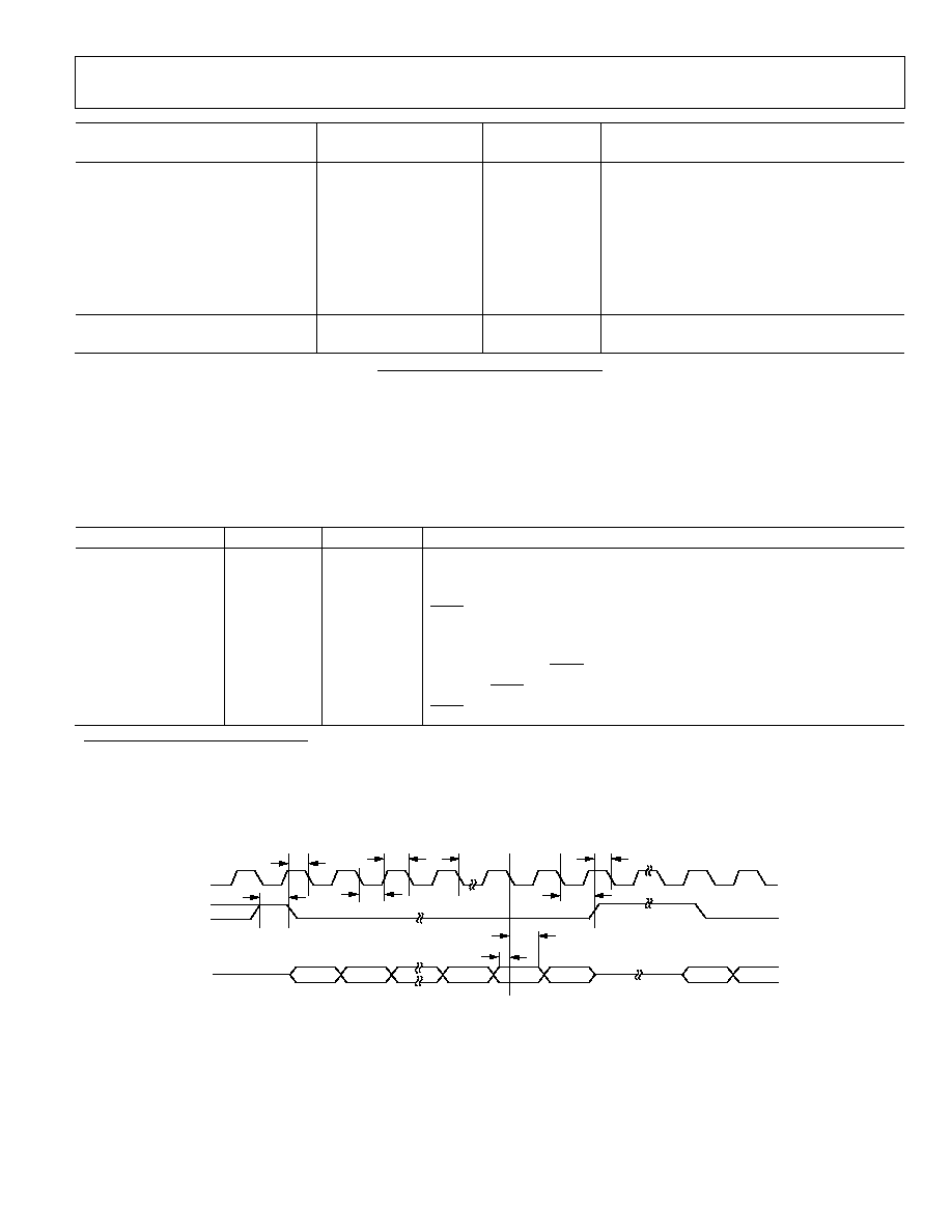
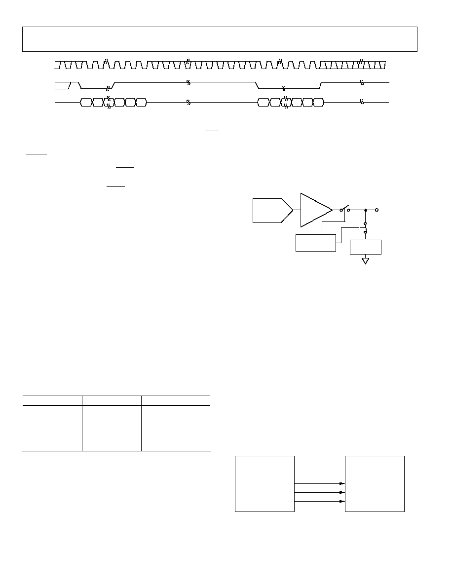
TIMING CHARACTERISTICS
V
DD
= 2.7 V to 5.5 V; all specifications T
MIN
to T
MAX
, unless otherwise noted. See Figure 2.
Table 3.
Parameter Limit
1
Unit Test
Conditions/Comments
t
1
2
33
ns min
SCLK cycle time
t
2
13
ns min
SCLK high time
t
3
12
ns min
SCLK low time
t
4
13 ns
min
SYNC to SCLK falling edge setup time
t
5
5
ns min
Data setup time
t
6
4.5
ns min
Data hold time
t
7
0 ns
min
SCLK falling edge to SYNC rising edge
t
8
33 ns
min
Minimum SYNC high time
t
9
13 ns
min
SYNC rising edge to next SCLK fall ignore
1
All input signals are specified with tr = tf = 1 ns/V (10% to 90% of V
DD
) and timed from a voltage level of (V
IL
+ V
IH
)/2.
2
Maximum SCLK frequency is 30 MHz.
t
4
t
3
t
2
t
5
t
7
t
6
D0
D1
D2
D14
D15
DIN
SYNC
SCLK
04783-C-002
t
9
t
1
t
8
D15
D14
Figure 2. Timing Diagram
AD5601/AD5611/AD5621
Preliminary Technical Data
Rev. PrC | Page 6 of 20
ABSOLUTE MAXIMUM RATINGS
T
A
= 25°C, unless otherwise noted.
Table 4.
Parameter Rating
V
DD
to GND
-0.3 V to +7.0 V
Digital Input Voltage to GND
0.3 V to V
DD
+ 0.3 V
V
OUT
to GND
0.3 V to V
DD
+ 0.3 V
Operating Temperature Range
Industrial (B Version)
40°C to +125°C
Storage Temperature Range
65°C to +160°C
Maximum Junction Temperature
150°C
SC70 Package
JA
Thermal Impedance
332°C/W
JC
Thermal Impedance
120°C/W
Lead Temperature, Soldering
Vapor Phase (60 s)
215°C
Infrared (15 s)
220°C
ESD 2.0
kV
Stresses above those listed under Absolute Maximum Ratings
may cause permanent damage to the device. This is a stress
rating only; functional operation of the device at these or any
other conditions above those listed in the operational sections
of this specification is not implied. Exposure to absolute
maximum rating conditions for extended periods may affect
device reliability.
ESD CAUTION
ESD (electrostatic discharge) sensitive device. Electrostatic charges as high as 4000 V readily accumulate on
the human body and test equipment and can discharge without detection. Although this product features
proprietary ESD protection circuitry, permanent damage may occur on devices subjected to high energy
electrostatic discharges. Therefore, proper ESD precautions are recommended to avoid performance
degradation or loss of functionality.
Preliminary Technical Data
AD5601/AD5611/AD5621
Rev. PrC | Page 7 of 20
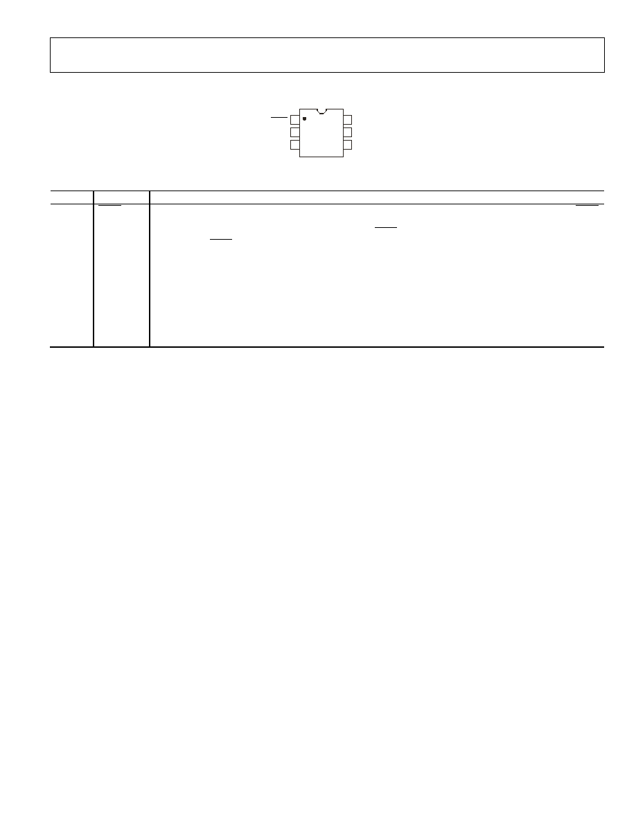
PIN CONFIGURATION AND FUNCTION DESCRIPTIONS
TOP VIEW
(Not to Scale)
V
DD
GND
SCLK
DIN
AD5601/
AD5611/
AD5621
V
OUT
SYNC 1
2
3
6
5
4
04783-C-003
Figure 3. 6-Lead SC70 Pin Configuration
Table 5. Pin Function Descriptions
Pin No.
Mnemonic
Function
1
SYNC
Level-Triggered Control Input (Active Low). This is the frame synchronization signal for the input data. When SYNC
goes low, it enables the input shift register, and data is transferred in on the falling edges of the clocks that follow.
The DAC is updated following the 16
th
clock cycle unless SYNC is taken high before this edge, in which case the
rising edge of SYNC acts as an interrupt and the write sequence is ignored by the DAC.
2 SCLK Serial Clock Input. Data is clocked into the input shift register on the falling edge of the serial clock input. Data can
be transferred at rates up to 30 MHz.
3 DIN Serial Data Input. This device has a 16-bit shift register. Data is clocked into the register on the falling edge of the
serial clock input.
4 V
DD
Power Supply Input. The AD5601/AD5611/AD5621 can be operated from 2.7 V to 5.5 V. V
DD
should be decoupled
to GND.
5
GND
Ground Reference Point for All Circuitry on the AD5601/AD5611/AD5621.
6 V
OUT
Analog Output Voltage from the DAC. The output amplifier has rail-to-rail operation.

AD5601/AD5611/AD5621
Preliminary Technical Data
Rev. PrC | Page 8 of 20
TERMINOLOGY
Relative Accuracy
For the DAC, relative accuracy or integral nonlinearity (INL) is
a measure of the maximum deviation, in LSBs, from a straight
line passing through the endpoints of the DAC transfer
function. A typical INL versus code plot can be seen in Figure 4.
Differential Nonlinearity
Differential nonlinearity (DNL) is the difference between the
measured change and the ideal 1 LSB change between any two
adjacent codes. A specified differential nonlinearity of ±1 LSB
maximum ensures monotonicity. This DAC is guaranteed
monotonic by design. A typical DNL versus code plot can be
seen in Figure 7.
Zero-Code Error
Zero-code error is a measure of the output error when zero
code (0x0000) is loaded to the DAC register. Ideally, the output
should be 0 V. The zero-code error is always positive in the
AD5601/AD5611/AD5621, because the output of the DAC
cannot go below 0 V. Zero-code error is due to a combination of
the offset errors in the DAC and output amplifier. Zero-code
error is expressed in mV. A plot of zero-code error versus
temperature can be seen in Figure 6.
Full-Scale Error
Full-scale error is a measure of the output error when full-scale
code (0xFFFF) is loaded to the DAC register. Ideally, the output
should be V
DD
- 1 LSB. Full-scale error is expressed in percent
of full-scale range. A plot of full-scale error versus temperature
can be seen in Figure 6.
Gain Error
Gain error is a measure of the span error of the DAC. It is the
deviation in slope of the DAC transfer characteristic from ideal,
expressed as a percent of the full-scale range.
Total Unadjusted Error
Total unadjusted error (TUE) is a measure of the output error
taking all the various errors into account. A typical TUE versus
code plot can be seen in Figure 5.
Zero-Code Error Drift
Zero-code error drift is a measure of the change in zero-code
error with a change in temperature. It is expressed in µV/°C.
Gain Error Drift
Gain error drift is a measure of the change in gain error with
changes in temperature. It is expressed in (ppm of full-scale
range)/°C.
Digital-to-Analog Glitch Impulse
Digital-to-analog glitch impulse is the impulse injected into the
analog output when the input code in the DAC register changes
state. It is normally specified as the area of the glitch in nV-s
and is measured when the digital input code is changed by
1 LSB at the major carry transition (0x7FFF to 0x8000). See
Figure 17.
Digital Feedthrough
Digital feedthrough is a measure of the impulse injected into
the analog output of the DAC from the digital inputs of the
DAC, but is measured when the DAC output is not updated. It is
specified in nV-s and is measured with a full-scale code change
on the data bus, that is, from all 0s to all 1s and vice versa.
Preliminary Technical Data
AD5601/AD5611/AD5621
Rev. PrC | Page 9 of 20
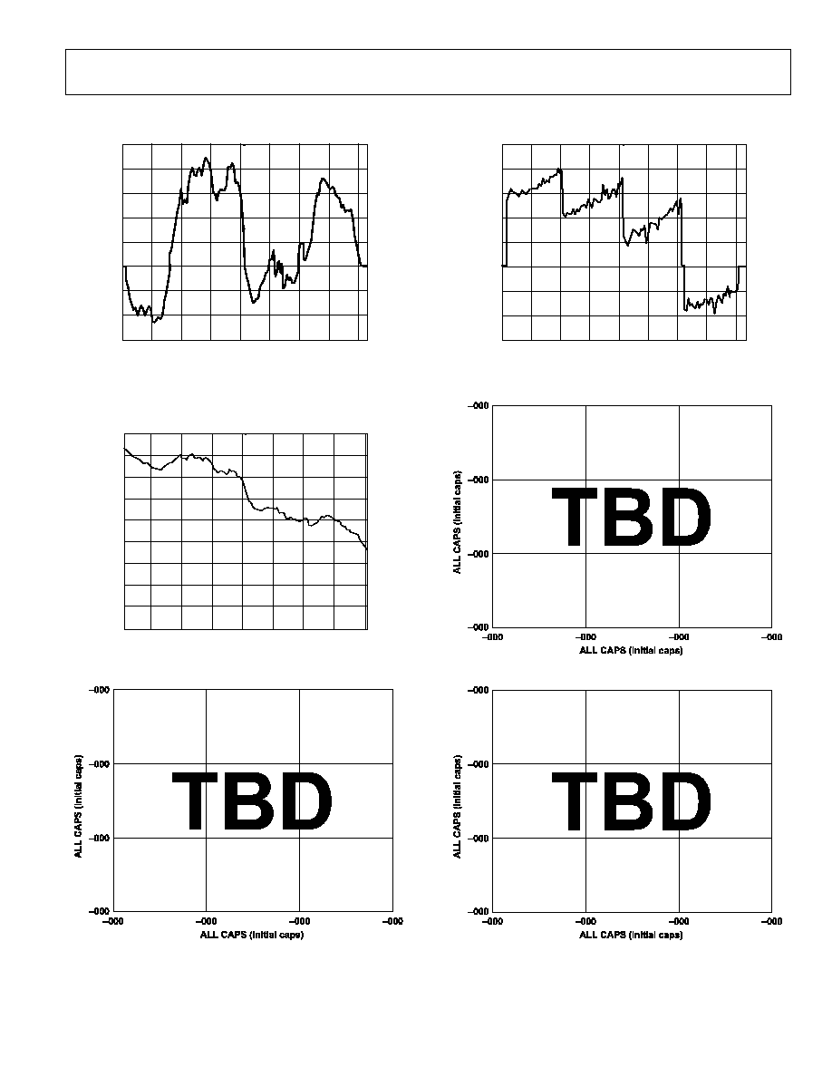
TYPICAL PERFORMANCE CHARACTERISTICS
CODE
04783-C-004
1.5
1.0
0.5
0
1.0
0.5
1.5
2.0
2.5
0
2k
4k
6k
8k
10k
12k
14k
16k
I
N
L
E
RRO
R (
L
S
B
s
)
Figure 4. Typical INL Plot
0
2
4
6
8
10
12
14
16
18
256
2k
4k
6k
8k
10k
12k
14k
16k
TUE (LS
B
s)
CODE
04783-C-005
Figure 5. Total Unadjusted Error
Figure 6. Zero-Scale Error and Full-Scale Error vs. Temperature
0.3
0.2
0.1
0
0.1
0.2
0.3
0.4
0.5
0
2k
4k
6k
8k
10k
12k
14k
16k
DNL E
RROR (LS
B
s
)
CODE
04783-C-007
Figure 7. Typical DNL Plot
Figure 8. INL and DNL vs. Supply
Figure 9. I
DD
Histogram @ V
DD
= 3 V/5 V
AD5601/AD5611/AD5621
Preliminary Technical Data
Rev. PrC | Page 10 of 20
0.6
0.4
0.2
0.0
0.2
0.4
0.6
0.8
15
10
5
0
5
10
15
I (mA)
V
O
(V
)
04783-C-010
DAC LOADED WITH FF CODE
V
DD
= 5V
T
A
= 25
°
C
DAC LOADED WITH 00 CODE
Figure 10. Source and Sink Current Capability
Figure 11. Supply Current vs. Temperature
Figure 12. Full-Scale Settling Time
Figure 13. Supply Current vs. Code
Figure 14. Supply Current vs. Supply Voltage
Figure 15. Half-Scale Settling Time
Preliminary Technical Data
AD5601/AD5611/AD5621
Rev. PrC | Page 11 of 20
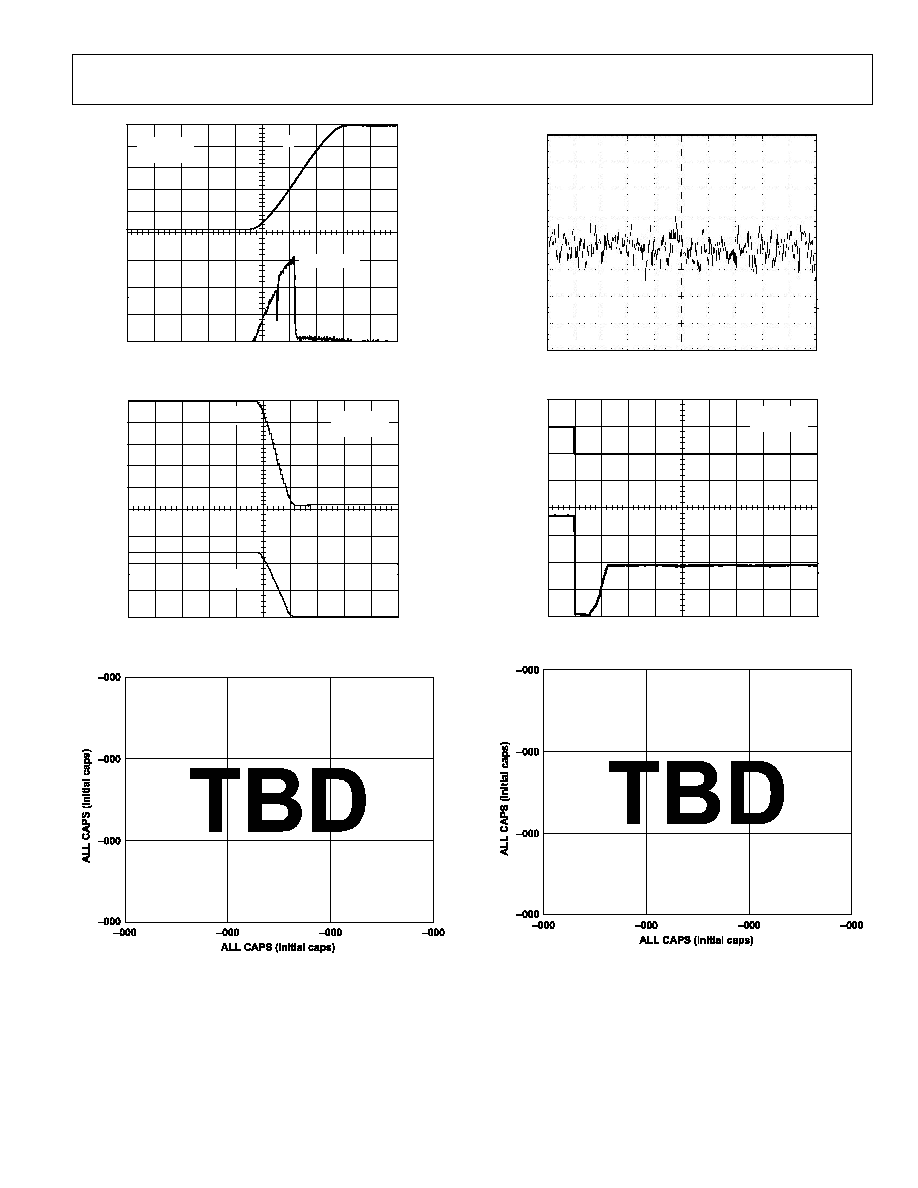
CH2
CH1
04783-C-016
V
DD
= 5V
T
A
= 25
°
C
V
DD
V
OUT
= 70mV
CH1 1V, CH2, TIME BASE = 20
µ
s/DIV
Figure 16. Power-On Reset to 0 V
CH1 1V, CH2 5V, TIME BASE = 50
µ
s/DIV
CH2
CH1
04783-C-017
V
DD
V
OUT
V
DD
= 5V
T
A
= 25
°
C
Figure 17. V
DD
vs. V
OUT
(Power-Down)
Figure 18. Digital-to-Analog Glitch Impulse
04611-A
-
019
CH1
V
DD
= 5V
T
A
= 25
°
C
MIDSCALE LOADED
CH1 5uV/DIV
Figure 19. 1/f Noise, 0.1 Hz to 10 Hz Bandwidth
CH1 5V, CH2 1V, TIME BASE = 5
µ
s/DIV
CH1
CH2
V
OUT
CLK
04783-C-020
V
DD
= 5V
T
A
= 25
°
C
Figure 20. Exiting Power-Down
Figure 21. Harmonic Distortion on Digitally Generated Waveform
AD5601/AD5611/AD5621
Preliminary Technical Data
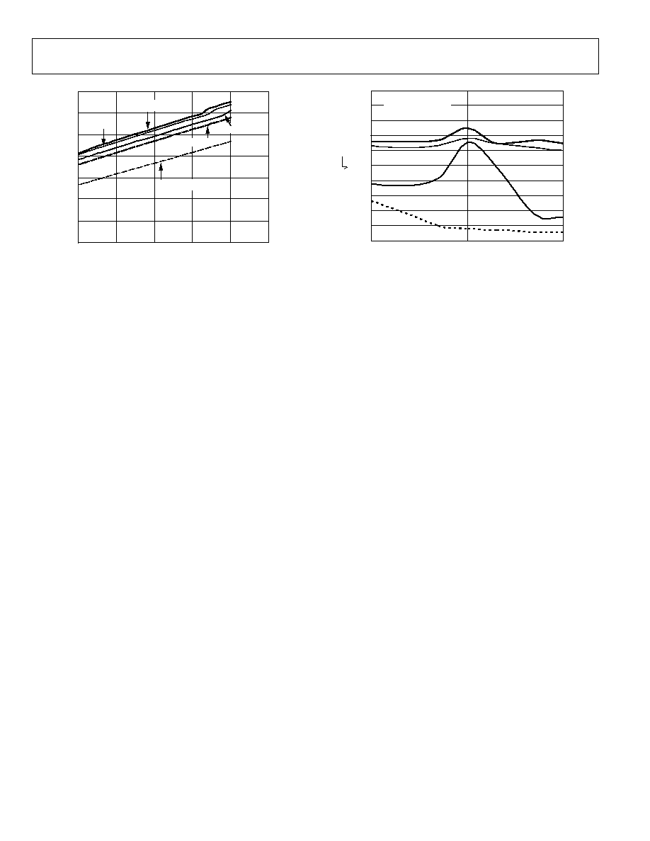
Rev. PrC | Page 12 of 20
0
20
40
60
80
100
120
140
0
5
10
15
20
25
FREQUENCY (MHz)
I
DD
(uA)
04783-C-023
3/4 SCALE
FULL SCALE
1/4 SCALE
MIDSCALE
ZERO SCALE
Figure 22.IDD vs. SCLK vs. Code
NOISE SPECTRAL
DENSITY
0
20
40
160
60
80
100
120
140
200
180
1K
10K
100K
FREQUENCY
CODE 0x2040
ZERO SCALE
MIDSCALE
FULL SCALE
04783-C-024
nV/
Hz
Figure 23. Noise Spectral Density
Preliminary Technical Data
AD5601/AD5611/AD5621
Rev. PrC | Page 13 of 20
GENERAL DESCRIPTION
D/A SECTION
The AD5601/AD5611/AD5621 DAC are fabricated on a CMOS
process. The architecture consists of a string DAC followed by
an output buffer amplifier. Figure 24 is a block diagram of the
DAC architecture.
V
DD
V
OUT
GND
RESISTOR
NETWORK
REF (+)
REF ()
OUTPUT
AMPLIFIER
DAC REGISTER
04783-C-025
Figure 24. DAC Architecture
Because the input coding to the DAC is straight binary, the ideal
output voltage is given by
×
=
N
DD
OUT
D
V
V
2
where D is the decimal equivalent of the binary code that is
loaded to the DAC register.
RESISTOR STRING
The resistor string section is shown in Figure 25. It is simply a
string of resistors, each of value R. The code loaded to the DAC
register determines at which node on the string the voltage is
tapped off to be fed into the output amplifier. The voltage is
tapped off by closing one of the switches connecting the string
to the amplifier. Because it is a string of resistors, it is
guaranteed monotonic.
R
R
R
R
R
TO OUTPUT
AMPLIFIER
04783-C-026
Figure 25. Resistor String Section
OUTPUT AMPLIFIER
The output buffer amplifier is capable of generating rail-to-rail
voltages on its output, giving an output range of 0 V to V
DD
. It is
capable of driving a load of 2 k in parallel with 1000 pF to
GND. The source and sink capabilities of the output amplifier
can be seen inFigure 10. The slew rate is 0.5 V/µs, with a half-
scale settling time of 8 µs with the output unloaded.
SERIAL INTERFACE
The AD5601/AD5611/AD5621 have a 3-wire serial interface
(SYNC, SCLK, and DIN) that is compatible with SPI, QSPI, and
MICROWIRE interface standards as well as most DSPs. See
Figure 2 for a timing diagram of a typical write sequence.
The write sequence begins by bringing the SYNC line low. Data
from the DIN line is clocked into the 16-bit shift register on the
falling edge of SCLK. The serial clock frequency can be as high
as 30 MHz, making the AD5601/AD5611/AD5621compatible
with high speed DSPs. On the 16
th
falling clock edge, the last
data bit is clocked in and the programmed function is executed
(a change in DAC register contents and/or a change in the
mode of operation). At this stage, the SYNC line might be kept
low or brought high. In either case, it must be brought high for a
minimum of 33 ns before the next write sequence so that a
falling edge of SYNC can initiate the next write sequence.
Because the SYNC buffer draws more current when V
IN
= 1.8 V
than it does when V
IN
= 0.8 V, SYNC should be idled low
between write sequences for even lower power operation of the
part, as mentioned above. However, it must be brought high
again just before the next write sequence.
INPUT SHIFT REGISTER
The input shift register is 16 bits wide (see Figure 26). The first
two bits are control bits that control which mode of operation
the power is in (normal mode or any one of three power-down
modes). For a complete description of the various modes, see
the Power-Down Modes section. The next 16 bits are the data
bits, which are transferred to the DAC register on the 16
th
falling
edge of SCLK.
DATA BITS
DB15 (MSB)
DB0 (LSB)
PD1
PD0
D13
D12
D11
D10
D9
D8
D7
D6
D5
D4
D3
D2
D1
D0
NORMAL OPERATION
1 k
TO GND
100 k
TO GND
THREE-STATE
POWER-DOWN MODES
0
0
1
1
0
1
0
1
04783-C
-
027
Figure 26. Input Register Contents
AD5601/AD5611/AD5621
Preliminary Technical Data
Rev. PrC | Page 14 of 20
04783-C-028
DIN
DB15
DB16
DB0
DB0
INVALID WRITE SEQUENCE:
SYNC HIGH BEFORE 16
TH
FALLING EDGE
VALID WRITE SEQUENCE, OUTPUT UPDATES
ON THE 16
TH
FALLING EDGE
SYNC
SCLK
Figure 27. SYNC Interrupt Facility
SYNC INTERRUPT
In a normal write sequence, the SYNC line is kept low for at
least 16 falling edges of SCLK and the DAC is updated on the
16
th
falling edge. However, if SYNC is brought high before the
16
th
falling edge, this acts as an interrupt to the write sequence.
The shift register is reset and the write sequence is seen as
invalid. Neither an update of the DAC register contents nor a
change in the operating mode occurs (see Figure 27).
POWER-ON RESET
The AD5601/AD5611/AD5621 contain a power-on reset circuit
that controls the output voltage during power-up. The DAC
register is filled with zeros and the output voltage is 0 V. It
remains there until a valid write sequence is made to the DAC.
This is useful in applications in which it is important to know
the state of the DAC's output while it is in the process of
powering up.
POWER-DOWN MODES
The AD5601/AD5611/AD5621 have four separate modes of
operation. These modes are software-programmable by setting
two bits (DB15 and DB14) in the control register. Table 6 shows
how the state of the bits corresponds to the mode of operation
of the device.
Table 6. Modes of Operation for the AD5601/AD5611/
AD5621
DB15 DB14 Operating
Mode
0 0 Normal
operation
Power-down
mode
0
1
1 k to GND
1
0
100 k to GND
1 1 Three-state
When both bits are set to 0, the part works normally with its
normal power consumption of 100 µA maximum at 5 V.
However, for the three power-down modes, the supply current
falls to <100 nA at 3 V. Not only does the supply current fall, but
the output stage is also internally switched from the output of
the amplifier to a resistor network of known values. This has the
advantage that the output impedance of the part is known while
the part is in power-down mode. There are three different
options: the output is connected internally to GND through a
1 k resistor or a 100 k resistor, or the output is left open-
circuited (three-state). Figure 28 shows the output stage.
POWER-DOWN
CIRCUITRY
RESISTOR
NETWORK
V
OUT
RESISTOR
STRING DAC
AMPLIFIER
04783-C-029
Figure 28. Output Stage During Power-Down
The bias generator, output amplifier, resistor string, and other
associated linear circuitry are all shut down when the power-
down mode is activated. However, the contents of the DAC
register are unaffected when in power-down. The time to exit
power-down is typically 2.5 µs for V
DD
= 5 V and 5 µs for
V
DD
= 3 V. See Figure 20 for a plot.
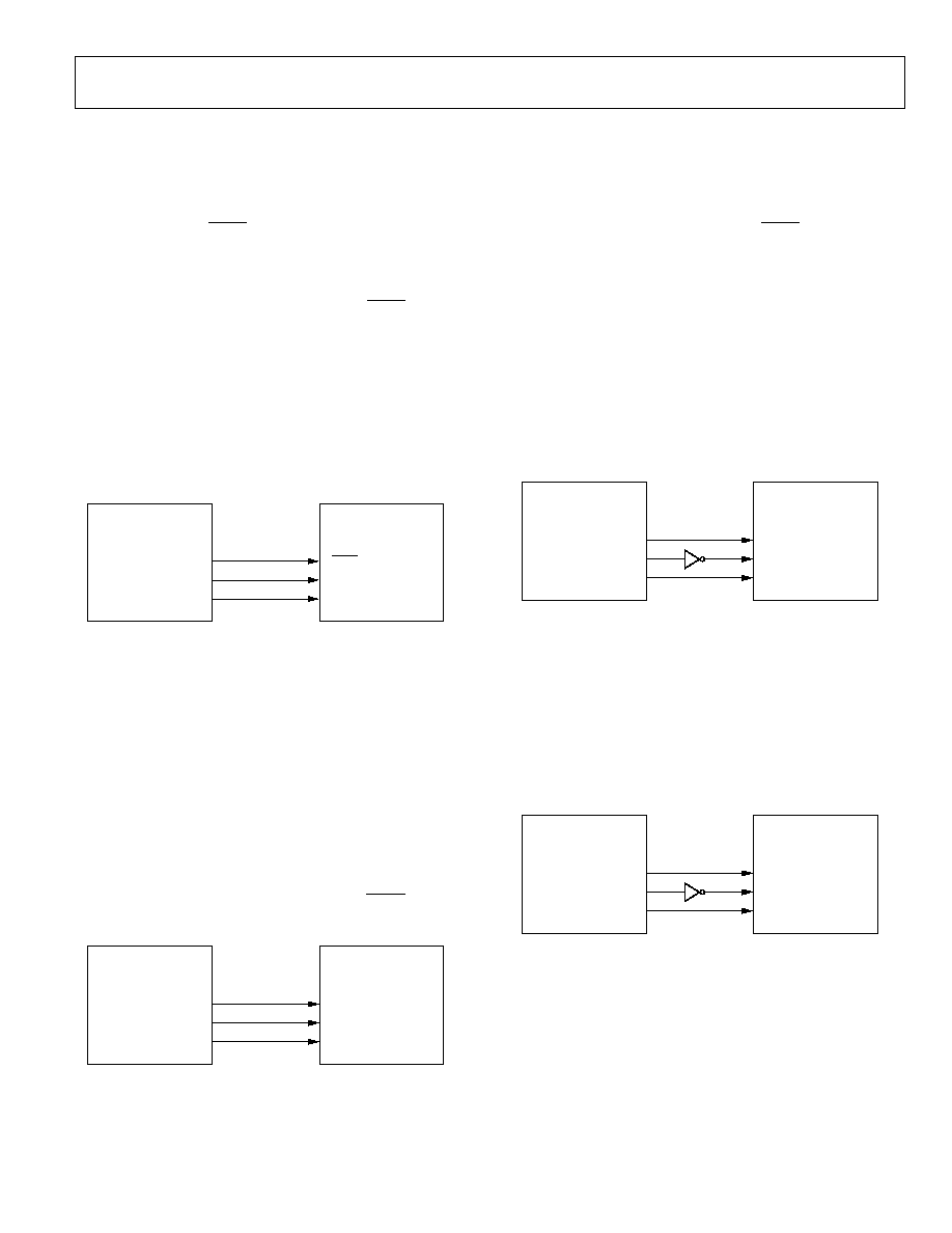
MICROPROCESSOR INTERFACING
AD5601/AD5611/AD5621 to ADSP-2101/ADSP-2103
Interface
Figure 29 shows a serial interface between the AD5601/
AD5611/AD5621 and the ADSP-2101/ADSP-2103. The
ADSP-2101/ADSP-2103 should be set up to operate in SPORT
transmit alternate framing mode. The ADSP-2101/ADSP-2103
SPORT are programmed through the SPORT control register
and should be configured as follows: internal clock operation,
active low framing, and 16-bit word length. Transmission is
initiated by writing a word to the Tx register after the SPORT
has been enabled.
ADSP-2101/
ADSP-2103*
AD5601/AD5611/
AD5621*
*ADDITIONAL PINS OMITTED FOR CLAIRTY
TFS
DT
SCLK
SYNC
DIN
SCLK
04783-C-030
Figure 29. AD5601/AD5611/AD5621 to ADSP-2101/ADSP-2103 Interface
Preliminary Technical Data
AD5601/AD5611/AD5621
Rev. PrC | Page 15 of 20
AD5601/AD5611/AD5621 to 68HC11/68L11 Interface
Figure 30 shows a serial interface between the AD5601/
AD5611/AD5621 and the 68HC11/68L11 microcontrollers.
SCK of the 68HC11/68L11 drives the SCLK of the AD5601/
AD5611/AD5621, while the MOSI output drives the serial data
line of the DAC. The SYNC signal is derived from a port line
(PC7). The setup conditions for correct operation of this
interface are as follows: the 68HC11/68L11 should be
configured so that its CPOL bit is a 0 and its CPHA bit is a 1.
When data is being transmitted to the DAC, the SYNC line is
taken low (PC7). When the 68HC11/68L11 is configured as
above, data appearing on the MOSI output is valid on the falling
edge of SCK. Serial data from the 68HC11/68L11 is transmitted
in 8-bit bytes with only eight falling clock edges occurring in
the transmit cycle. Data is transmitted MSB first. To load data to
the AD5601/AD5611/AD5621, PC7 is left low after the first
eight bits are transferred, and a second serial write operation is
performed to the DAC. PC7 is taken high at the end of this
procedure.
68HC11/
68L11
AD5601/AD5611/
AD5621*
*ADDITIONAL PINS OMITTED FOR CLAIRTY
PC7
SCK
MOSI
SYNC
SCLK
DIN
04783-C-031
Figure 30. AD5601/AD5611/AD5621 to 68HC11/68L11 Interface
AD5601/AD5611/AD5621 to Blackfin® ADSP-BF53X
Interface
Figure 31 shows a serial interface between the AD5601/
AD5611/AD5621 and the Blackfin ADSP-BF53x
microprocessors. The ADSP-BF53x processor family
incorporates two dual-channel synchronous serial ports,
SPORT1 and SPORT0, for serial and multiprocessor
communications. Using SPORT0 to connect to the AD5601/
AD5611/AD5621, the setup for the interface is as follows:
DT0PRI drives the SDIN pin of the AD5601/AD5611/AD5621,
while TSCLK0 drives the SCLK of the part. The SYNC is driven
from TFS0.
ADSP-BF53X
AD5601/AD5611/
AD5621
*ADDITIONAL PINS OMITTED FOR CLAIRTY
DT0PRI
TSCLK0
TFS0
DIN
SCLK
SYNC
04783-C-032
Figure 31. AD5601/AD5611/AD5621 to Blackfin ADSP-BF53X Interface
AD5601/AD5611/AD5621 to 80C51/80L51 Interface
Figure 32 shows a serial interface between the AD5601/
AD5611/AD5621 and the 80C51/80L51 microcontroller. The
setup for the interface is as follows: TXD of the 80C51/80L51
drives SCLK of the AD5601/AD5611/AD5621, while RXD
drives the serial data line of the part. The SYNC signal is again
derived from a bit programmable pin on the port. In this case,
port line P3.3 is used. When data is to be transmitted to the
AD5601/AD5611/AD5621, P3.3 is taken low. The 80C51/80L51
transmit data only in 8-bit bytes; thus, only eight falling clock
edges occur in the transmit cycle. To load data to the DAC, P3.3
is left low after the first eight bits are transmitted, and a second
write cycle is initiated to transmit the second byte of data. P3.3
is taken high following the completion of this cycle. The 80C51/
80L51 output the serial data in a format that has the LSB first.
The AD5601/AD5611/AD5621 require their data with the MSB
as the first bit received. The 80C51/80L51 transmit routine
should take this into account.
80C51/80L51*
AD5601/AD5611/
AD5621*
*ADDITIONAL PINS OMITTED FOR CLAIRTY
P3.3
TXD
RXD
SYNC
SCLK
DIN
04783-C-033
Figure 32. AD5601/AD5611/AD5621 to 80C51/80L51 Interface
AD5601/AD5611/AD5621 to MICROWIRE Interface
Figure 33 shows an interface between the AD5601/AD5611/
AD5621 and any MICROWIRE compatible device. Serial data is
shifted out on the falling edge of the serial clock and is clocked
into the AD5601/AD5611/AD5621 on the rising edge of the SK.
MICROWIRE*
AD5601/AD5611/
AD5621*
*ADDITIONAL PINS OMITTED FOR CLAIRTY
CS
SK
SO
SYNC
SCLK
DIN
04783-C-034
Figure 33. AD5601/AD5611/AD5621 to MICROWIRE Interface
AD5601/AD5611/AD5621
Preliminary Technical Data
Rev. PrC | Page 16 of 20
APPLICATIONS
CHOOSING A REFERENCE AS POWER SUPPLY FOR
AD5601/AD5611/AD5621
The AD5601/AD5611/AD5621 come in a tiny SC70 package
with less than 100 µA supply current. Because of this, the choice
of reference depends on the application requirement. For space-
saving applications, the ADR425 is available in an SC70 package
and has excellent drift at 3 ppm/°C. It also provides very good
noise performance at 3.4 µV p-p in the 0.1 Hz to 10 Hz range.
Because the supply current required by the AD5601/AD5611/
AD5621 is extremely low, the parts are ideal for low supply
applications. The ADR293 voltage reference is recommended in
this case. This requires 15 µA of quiescent current and can,
therefore, drive multiple DACs in one system, if required.
3-WIRE
SERIAL
INTERFACE
SYNC
SCLK
DIN
7V
5V
V
OUT
= 0V TO 5V
ADR425
04783-C-035
AD5601/AD5611/
AD5621
Figure 34. ADR425 as Power Supply to the AD5601/AD5611/AD5621
Some recommended precision references for use as supplies to
the AD5601/AD5611/AD5621 are listed in Table 7.
Table 7. Precision References for Use with AD5601/AD5611/
AD5621
Part
No.
Initial
Accuracy
(mV max)
Temperature
Drift
(ppm/°C max)
0.1 Hz to 10 Hz
Noise (µV p-p typ)
ADR435 ±6
3
3.4
ADR425 ±6
3
3.4
ADR02 ±5
3
15
ADR395 ±6
25
5
BIPOLAR OPERATION USING THE AD5601/
AD5611/AD5621
The AD5601/AD5611/AD5621 have been designed for single-
supply operation, but a bipolar output range is also possible
using the circuit in Figure 35. The circuit in Figure 35 gives an
output voltage range of ±5 V. Rail-to-rail operation at the
amplifier output is achievable using an AD820 or OP295 as the
output amplifier.
The output voltage for any input code can be calculated as
follows:
×
-
+
×
×
=
R1
R2
V
R1
R2
R1
D
V
V
DD
N
DD
O
2
where D represents the input code in decimal (02
N
).
With V
DD
= 5 V, R1 = R2 = 10 k:
V
5
2
10
-
×
=
N
O
D
V
This is an output voltage range of ±5 V with 0x0000 corre-
sponding to a 5 V output, and 0x3FFF corresponding to a
+5 V output.
R2 = 10k
04783-C-036
+5V
5V
AD820/
OP295
3-WIRE
SERIAL
INTERFACE
+5V
AD5601/AD5611/
AD5621
10
µ
F
0.1
µ
F
V
DD
V
OUT
R1 = 10k
5V
Figure 35. Bipolar Operation with the AD5601/AD5611/AD5621
Preliminary Technical Data
AD5601/AD5611/AD5621
Rev. PrC | Page 17 of 20
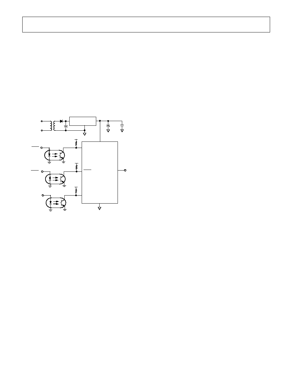
USING AD5601/AD5611/AD5621 WITH AN OPTO-
ISOLATED INTERFACE
In process-control applications in industrial environments, it is
often necessary to use an opto-isolated interface to protect and
isolate the controlling circuitry from any hazardous common-
mode voltages that might occur in the area where the DAC is
functioning. Opto-isolators provide isolation in excess of 3 kV.
Because the AD5601/AD5611/AD5621 use a 3-wire serial logic
interface, they require only three opto-isolators to provide the
required isolation (see Figure 36). The power supply to the parts
also needs to be isolated. This is done by using a transformer.
On the DAC side of the transformer, a 5 V regulator provides
the 5 V supply required for the AD5601/AD5611/AD5621.
V
DD
0.1
µ
F
V
DD
V
DD
10k
10k
10k
+5V
REGULATOR
V
OUT
GND
04783-C-037
DIN
SYNC
SCLK
POWER
10
µ
F
V
DD
SYNC
SCLK
DATA
AD5601/
AD5611/
AD5621
Figure 36. AD5601/AD5611/AD5621 with an Opto-Isolated Interface
POWER SUPPLY BYPASSING AND GROUNDING
When accuracy is important in a circuit, it is helpful to carefully
consider the power supply and ground return layout on the
board. The printed circuit board containing the AD5601/
AD5611/AD5621 should have separate analog and digital
sections, each having its own area of the board. If the AD5601/
AD5611/AD5621 are in a system where other devices require an
AGND to DGND connection, the connection should be made
at one point only. This ground point should be as close to the
AD5601/AD5611/AD5621 as possible.
The power supply to the AD5601/AD5611/AD5621 should be
bypassed with 10 µF and 0.1 µF capacitors. The capacitors
should be physically as close as possible to the device, with the
0.1 µF capacitor ideally right up against the device. The 10 µF
capacitors are the tantalum bead type. It is important that the
0.1 µF capacitor have low effective series resistance (ESR) and
effective series inductance (ESI), such as in common ceramic
types of capacitors. This 0.1 µF capacitor provides a low
impedance path to ground for high frequencies caused by
transient currents due to internal logic switching.
The power supply line itself should have as large a trace as
possible to provide a low impedance path and reduce glitch
effects on the supply line. Clocks and other fast switching digital
signals should be shielded from other parts of the board by
digital ground. Avoid crossover of digital and analog signals, if
possible. When traces cross on opposite sides of the board,
ensure that they run at right angles to each other to reduce
feedthrough effects through the board. The best board layout
technique is the microstrip technique where the component
side of the board is dedicated to the ground plane only and the
signal traces are placed on the solder side. However, this is not
always possible with a 2-layer board.
AD5601/AD5611/AD5621
Preliminary Technical Data
Rev. PrC | Page 18 of 20
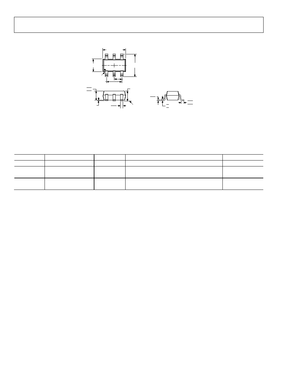
OUTLINE DIMENSIONS
0.22
0.08
0.46
0.36
0.26
8°
4°
0°
0.30
0.15
1.00
0.90
0.70
SEATING
PLANE
1.10 MAX
2.00 BSC
PIN 1
2.10 BSC
0.65 BSC
1.25 BSC
1.30 BSC
0.10 MAX
0.10 COPLANARITY
COMPLIANT TO JEDEC STANDARDS MO-203AB
3
5
4
2
6
1
Figure 37. 6-Lead Plastic Surface Mount Package [SC70]
(KS-6)
Dimensions shown in millimeters
ORDERING GUIDE
Model Temperature
Range
Description
Package Description
Package Option
AD5601BKS
40°C to +125°C
±0.5 LSB INL
6-Lead Plastic Surface Mount Package (SC70)
KS-6
AD5611BKS
40°C to +125°C
±0.5 LSB INL
6-Lead Plastic Surface Mount Package (SC70)
KS-6
AD5611AKS
40°C to +125°C
±4.0 LSB INL
6-Lead Plastic Surface Mount Package (SC70)
KS-6
AD5621BKS
40°C to +125°C
±1.0 LSB INL
6-Lead Plastic Surface Mount Package (SC70)
KS-6
AD5621AKS
40°C to +125°C
±6.0 LSB INL
6-Lead Plastic Surface Mount Package (SC70)
KS-6

Preliminary Technical Data
AD5601/AD5611/AD5621
Rev. PrC | Page 19 of 20
NOTES

AD5601/AD5611/AD5621
Preliminary Technical Data
Rev. PrC | Page 20 of 20
NOTES
© 2004 Analog Devices, Inc. All rights reserved. Trademarks and
registered trademarks are the property of their respective owners.
PR0478306/04(PrC)
Document Outline
- FEATURES
- APPLICATIONS
- FUNCTIONAL BLOCK DIAGRAM
- GENERAL DESCRIPTION
- þÿ
- þÿ
- þÿ
- þÿ
- þÿ
- þÿ
- þÿ
- þÿ
- þÿ