 | ÐлекÑÑоннÑй компоненÑ: AD5663 | СкаÑаÑÑ:  PDF PDF  ZIP ZIP |
AD5663 2.7 V to 5.5 V, 500 µA, Rail-to-Rail Output Dual 16-Bit nanoDAC in 10-Lead MSOP Preliminary Data Sheet (Rev. PrA)
2.7 V to 5.5 V, 500 µA, Rail-to-Rail Output
Dual 16-Bit nanoDAC
TM
in 10-Lead MSOP
Preliminary Technical Data
AD5663
Rev. PrA
Information furnished by Analog Devices is believed to be accurate and reliable.
However, no responsibility is assumed by Analog Devices for its use, nor for any
infringements of patents or other rights of third parties that may result from its use.
Specifications subject to change without notice. No license is granted by implication
or otherwise under any patent or patent rights of Analog Devices. Trademarks and
registered trademarks are the property of their respective owners.
One Technology Way, P.O. Box 9106, Norwood, MA 02062-9106, U.S.A.
Tel: 7101.329.4700
www.analog.com
Fax: 7101.326.10703
© 2005 Analog Devices, Inc. All rights reserved.
FEATURES
Low power dual 16-bit nanoDAC
10-lead MSOP and 3mmx3mm LFCSP package
Power-down to 480 nA @ 5 V, 100 nA @ 3 V
2.7 V to 5.5 V power supply
Guaranteed 16-bit monotonic by design
3 power-down functions
Hardware /LDAC and /CLR functions
Serial interface with Schmitt-triggered inputs
Rail-to-rail operation
SYNC interrupt facility
APPLICATIONS
Process control
Data acquisition systems
Portable battery-powered instruments
Digital gain and offset adjustment
Programmable voltage and current sources
Programmable attenuators
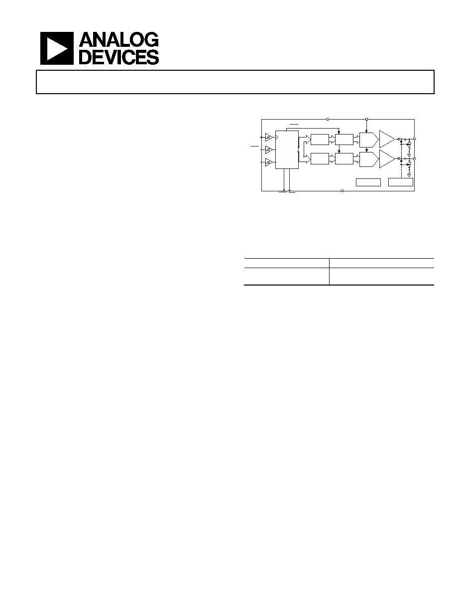
FUNCTIONAL BLOCK DIAGRAM
INPUT
REGISTER
VOUTA
BUFFER
DAC
REGISTER
STRING
DAC A
VDD
VREF
INPUT
REGISTER
VOUTB
BUFFER
DAC
REGISTER
POWER-ON
RESET
POWER-DOWN
LOGIC
LDAC
STRING
DAC B
GND
AD5663
DIN
SYNC
SCLK
LDAC CLR
INTERFACE
LOGIC
Figure 1.
RELATED DEVICES
Part No.
Description
AD5643R/ AD5663R
3 V/5 V 14- 16-bit DAC with
internal reference
GENERAL DESCRIPTION
The AD5663, a member of the nanoDAC family is a low power,
dual, 16-bit buffered voltage-out DAC that operates from a
single 2.7 V to 5.5 V supply and is guaranteed monotonic by
design.
The AD5663 requires an external reference voltage to set the
output range of the DAC. The part incorporates a power-on
reset circuit that ensures the DAC output powers up to 0 V or
midscale (AD5663-1) and remains there until a valid write takes
place. The part contains a power-down feature that reduces the
current consumption of the device to 480 nA at 5 V and
provides software-selectable output loads while in power-down
mode.
The low power consumption of this part in normal operation
makes it ideally suited to portable battery-operated equipment.
The power consumption is 3 mW at 5 V, going down to 2.4 µW
in power-down mode.
The AD5663's on-chip precision output amplifier allows rail-to-
rail output swing to be achieved.
The AD5663 uses a versatile 3-wire serial interface that operates
at clock rates up to 50 MHz, and is compatible with standard
SPI®, QSPITM, MICROWIRETM, and DSP interface standards.
PRODUCT HIGHLIGHTS
1.
16-bit DAC
2.
Available in 10-lead MSOP and 10-lead 3mmx3mm
LFCSP package.
3.
Low power. Typically consumes 1.5 mW at 3 V and 3 mW
at 5 V.
4.
10 µs max settling time.

AD5663
Preliminary Technical Data
Rev. PrA | Page 2 of 29
TABLE OF CONTENTS
Specifications..................................................................................... 3
Timing Characteristics..................................................................... 6
Absolute Maximum Ratings............................................................ 6
ESD Caution.................................................................................. 7
Pin Configuration and Function Description .............................. 8
Typical Performance Characteristics ............................................. 9
Terminology .................................................................................... 14
Theory of Operation ...................................................................... 16
D/A Section................................................................................. 16
Resistor String ............................................................................. 16
Output Amplifier........................................................................ 16
Serial Interface ............................................................................ 16
Input Shift Register..................................................................... 17
SYNC
Interrupt .......................................................................... 17
Power-On Reset.......................................................................... 17
Power-Down Modes .................................................................. 18
Microprocessor Interfacing....................................................... 21
Applications..................................................................................... 23
Choosing a Reference for the AD5663.................................... 23
Using a Reference as a Power Supply for the AD5663 .......... 23
Bipolar Operation Using the AD5663 ..................................... 24
Using AD5663 with a Galvanically Isolated Interface........... 24
Power Supply Bypassing and Grounding................................ 25
Outline Dimensions ....................................................................... 26
Ordering Guide .......................................................................... 27
REVISION HISTORY
Xx/05--Revision 0: Initial Version

Preliminary Technical Data
AD5663
Rev. PrA
| Page 3 of 29
SPECIFICATIONS
(V
DD
= +2.7 V to +5.5 V; R
L
= 2 k to GND; C
L
= 200 pF to GND; V
REF
= V
DD
; all specifications T
MIN
to T
MAX
unless otherwise noted)
Table 1.
Parameter A
Grade
3
B
Grade
3
Unit
Conditions/Comments
STATIC PERFORMANCE
1
Resolution
16
16
Bits min
Relative Accuracy
±32
tbd
LSB max
Differential Nonlinearity
±1
±1
LSB max
Guaranteed Monotonic by Design.
Load Regulation
2
2
LSB/mA
VDD=Vref=5V, Midscale Iout=0mA to 15mA
sourcing/sinking
LSB/mA
VDD=Vref=3V, Midscale Iout=0mA to 7.5mA
sourcing/sinking
Zero Code Error
+2
+2
mV typ
All Zeroes Loaded to DAC Register
+10
+10
mV
max
Offset Error
±10
±10
mV max
Full-Scale Error
-0.15
-0.15
% of FSR typ
All Ones Loaded to DAC Register.
-1
-1
% of FSR max
Gain Error
±1. 5
±1. 5
% of FSR max
Zero Code Error Drift
2
±2
±2
µV/°C
typ
Gain Temperature Coefficient
±2.5
±2.5
ppm typ
of FSR/°C
Offset Temperature Coefficient 1.7
1.7
µV/°C typ
DC Power Supply Rejection Ratio
-100
-100
dB typ
DAC code = midscale; V
DD
= 5V ±10%
DC Crosstalk
6
10 10
µV typ
R
L
= 2 k. to GND or V
DD
4.5 4.5
µV/mA typ
Due to Load current change
-10 -10
µV typ
Due to Powering Down (per channel)
OUTPUT CHARACTERISTICS
1
Output Voltage Range
0 0
V min
V
DD
V
DD
V max
Capacitive Load Stability
2
2
nF typ
R
L
=
10
10
nF
typ
R
L
=2 k
DC Output Impedance
0.5
0.5
typ
Short Circuit Current
30
30
mA typ
V
DD
=+5V
Power-Up Time
4
4
µs typ
Coming Out of Power-Down Mode. V
DD
=+5V
REFERENCE INPUT
Reference Input voltage
V
DD
V
DD
V
±1% for specified performance
Reference Current
40
40
µA typ
V
REF
= V
DD
= 5 V
75
75
µA max
Reference Current
30
30
µA typ
V
REF
= V
DD
= 3.6 V
50
50
µA max
Reference Input Range
0.75
0.75
V min
V
DD
V
DD
V max
Reference Input Impedance
150
150
k
typ
Per DAC channel
LOGIC INPUTS
2
Input Current
±2
±2
µA max
All digital inputs
V
INL
, Input Low Voltage
0.8
0.8
V max
V
DD
=+5 V, +3 V
V
INH
, Input High Voltage
2
2
V min
V
DD
=+5 V, +3 V
1
Linearity calculated using a reduced code range: AD5663 ( Code 512 to code 65024);. Output unloaded.
2
Guaranteed by design and characterization, not production tested.
3
. Temperature Range: A grade (-40°C to +105°C); B grade (-40°C to +105°C);
AD5663
Preliminary Technical Data
Rev. PrA | Page 4 of 29
Parameter A
Grade
3
B
Grade
3
Unit
Conditions/Comments
Pin Capacitance
3
3
pF typ
POWER REQUIREMENTS
V
DD
2.7
2.7
V min
All Digital Inputs at 0 or V
DD
5.5
5.5
V max
DAC Active and Excluding Load Current
I
DD
(Normal Mode)
V
DD
=4.5 V to +5.5 V
0.6
0.6
mA typ
V
IH
=V
DD
and V
IL
=GND
V
DD
=4.5 V to +5.5 V
0.9
0.9
mA max
V
IH
=V
DD
and V
IL
=GND
V
DD
=2.7V to +3.6 V
0.5
0.5
mA typ
V
IH
=V
DD
and V
IL
=GND
V
DD
=2.7V to +3.6 V
0.7
0.7
mA max
V
IH
=V
DD
and V
IL
=GND
I
DD
(All Power-Down Modes)
V
DD
=4.5 V to +5.5 V
0.48
0.48
µA typ
V
IH
=V
DD
and V
IL
=GND
V
DD
=4.5 V to +5.5 V
1
1
µA max
V
IH
=V
DD
and V
IL
=GND
V
DD
=2.7V to +3.6V
0.1
0.1
µA typ
V
IH
=V
DD
and V
IL
=GND
V
DD
=2.7V to +3.6V
1
1
µA max
V
IH
=V
DD
and V
IL
=GND
POWER EFFICIENCY
I
OUT
/I
DD
90
90
%
I
LOAD
=2 mA, V
DD
=+5 V
4
Output unloaded.
5
Reference input range at ambient where ±1 LSB max DNL specification is achievable.

Preliminary Technical Data
AD5663
Rev. PrA
| Page 5 of 29
AC CHARACTERISTICS
1
(V
DD
= +2.7 V to +5.5 V; R
L
= 2 k to GND; C
L
= 200 pF to GND; Vref = V
DD
; all specifications T
MIN
to T
MAX
unless otherwise noted)
Parameter
2
Min
Typ
Max
Unit
Conditions/Comments
Output Voltage Settling Time
8
10
µs
¼ to ¾ scale settling to ±2LSB
Settling Time for 1LSB Step
Slew Rate
1.5
V/µs
Digital-to-Analog Glitch Impulse
10
nV-s
1 LSB Change Around Major Carry.
Channel to-Channel Isolation
100
dB
Digital Feedthrough
0.5
nV-s
Digital Crosstalk
0.5
nV-s
Analog Crosstalk
1
nV-s
DAC-to-DAC Crosstalk
3
nV-s
Multiplying Bandwidth
200
kHz
VREF = 2V ± 0.1 V p-p.
Total Harmonic Distortion
-80
dB
VREF = 2V ± 0.1 V p-p. Frequency = 10kHz
Output Noise Spectral Density
120
nV/Hz
DAC code=8400
H
, 1kHz
100
nV/Hz
DAC code=8400
H
, 10kHz
Output Noise
15
µVp-p
0.1Hz to 10Hz;
NOTES
1
Guaranteed by design and characterization; not production tested.
2
See the Terminology section.
3
Temperature range (Y Version): 40
°C to +125°C; typical at +25°C.