 | –≠–ª–µ–∫—Ç—Ä–æ–Ω–Ω—ã–π –∫–æ–º–ø–æ–Ω–µ–Ω—Ç: AD568S | –°–∫–∞—á–∞—Ç—å:  PDF PDF  ZIP ZIP |

FUNCTIONAL BLOCK DIAGRAM
REV. A
Information furnished by Analog Devices is believed to be accurate and
reliable. However, no responsibility is assumed by Analog Devices for its
use, nor for any infringements of patents or other rights of third parties
which may result from its use. No license is granted by implication or
otherwise under any patent or patent rights of Analog Devices.
a
12-Bit Ultrahigh Speed
Monolithic D/A Converter
AD568
FEATURES
Ultrahigh Speed: Current Settling to 1 LSB in 35 ns
High Stability Buried Zener Reference on Chip
Monotonicity Guaranteed Over Temperature
10.24 mA Full-Scale Output Suitable for Video
Applications
Integral and Differential Linearity Guaranteed Over
Temperature
0.3" "Skinny DIP" Packaging
Variable Threshold Allows TTL and CMOS
Interface
MIL-STD-883 Compliant Versions Available
PRODUCT DESCRIPTION
The AD568 is an ultrahigh-speed, 12-bit digital-to-analog con-
verter (DAC) settling to 0.025% in 35 ns. The monolithic de-
vice is fabricated using Analog Devices' Complementary Bipolar
(CB) Process. This is a proprietary process featuring high-speed
NPN and PNP devices on the same chip without the use of di-
electric isolation or multichip hybrid techniques. The high speed
of the AD568 is maintained by keeping impedance levels low
enough to minimize the effects of parasitic circuit capacitances.
The DAC consists of 16 current sources configured to deliver a
10.24 mA full-scale current. Multiple matched current sources
and thin-film ladder techniques are combined to produce bit
weighting. The DAC's output is a 10.24 mA full scale (FS) for
current output applications or a 1.024 V FS unbuffered voltage
output. Additionally, a 10.24 V FS buffered output may be gen-
erated using an onboard 1 k
span resistor with an external op
amp. Bipolar ranges are accomplished by pin strapping.
Laser wafer trimming insures full 12-bit linearity. All grades of
the AD568 are guaranteed monotonic over their full operating
temperature range. Furthermore, the output resistance of the
DAC is trimmed to 100
±
1.0%. The gain temperature coeffi-
cient of the voltage output is 30 ppm/
∞
C max (K).
The AD568 is available in three performance grades. The
AD568JQ and KQ are available in 24-pin cerdip (0.3") packages
and are specified for operation from 0
∞
C to +70
∞
C. The
AD568SQ features operation from ≠55
∞
C to +125
∞
C and is also
packaged in the hermetic 0.3" cerdip.
One Technology Way, P.O. Box 9106, Norwood, MA 02062-9106, U.S.A.
Tel: 617/329-4700
Fax: 617/326-8703
PRODUCT HIGHLIGHTS
1. The ultrafast settling time of the AD568 allows leading edge
performance in waveform generation, graphics display and
high speed A/D conversion applications.
2. Pin strapping provides a variety of voltage and current output
ranges for application versatility. Tight control of the abso-
lute output current reduces trim requirements in externally-
scaled applications.
3. Matched on-chip resistors can be used for precision scaling in
high speed A/D conversion circuits.
4. The digital inputs are compatible with TTL and +5 V
CMOS logic families.
5. Skinny DIP (0.3") packaging minimizes board space require-
ments and eases layout considerations.
6. The AD568 is available in versions compliant with MIL-
STD-883. Refer to the Analog Devices Military Products
Databook or current AD568/883B data sheet for detailed
specifications.

Model
AD568J
AD568K
AD568S
Min
Typ
Max
Min
Typ
Max
Min
Typ
Max
Units
RESOLUTION
12
12
12
Bits
ACCURACY
1
Linearity
≠1/2
+1/2
≠1/4
+1/4
≠1/2
+1/2
LSB
T
MIN
to T
MAX
≠3/4
+3/4
≠1/2
+1/2
≠3/4
+3/4
LSB
Differential Nonlinearity
≠1
+1
≠1/2
+1/2
≠1
+1
LSB
T
MIN
to T
MAX
≠1
+1
≠1
+ 1
≠1
≠1
LSB
Monotonicity
GUARANTEED OVER RATED SPECIFICATION TEMPERATURE RANGE
Unipolar Offset
≠0.2
+0.2
*
*
*
*
% of FSR
Bipolar Offset
≠1.0
+1.0
*
*
*
*
% of FSR
Bipolar Zero
≠0.2
+0.2
*
*
*
*
% of FSR
Gain Error
≠1.0
+1.0
*
*
*
*
% of FSR
TEMPERATURE COEFFICIENTS
2
Unipolar Offset
≠5
+5
≠3
+3
≠5
+5
ppm of FSR/
∞
C
Bipolar Offset
≠30
+30
≠20
+20
≠30
+30
ppm of FSR/
∞
C
Bipolar Zero
≠15
+15
∑
∑
∑
∑
ppm of FSR/
∞
C
Gain Drift
≠50
+50
≠30
+30
≠50
+50
ppm of FSR/
∞
C
Gain Drift (I
OUT
)
≠150
+150
*
*
*
*
ppm of FSR/
∞
C
DATA INPUTS
Logic Levels (T
MIN
to T
MAX
)
V
IH
2.0
7.0
*
*
*
*
V
V
IL
0.0
0.8
*
*
*
*
V
Logic Currents (T
MIN
to T
MAX
)
I
IH
≠10
0
+10
*
*
*
*
*
*
µ
A
I
IL
≠0.5
≠60
≠100
*
*
*
*
≠100
≠200
µ
A
V
TH
Pin Voltage
1.4
*
*
V
CODING
BINARY, OFFSET BINARY
CURRENT OUTPUT RANGES
0 to 10.24,
±
5.12
mA
VOLTAGE OUTPUT RANGES
0 to 1.024,
±
0.512
V
COMPLIANCE VOLTAGE
≠2
+1.2
*
*
*
*
V
OUTPUT RESISTANCE
Exclusive of R
L
160
200
240
*
*
Inclusive of R
L
99
100
101
*
*
SETTLING TIME
Current to
±
0.025%
35
*
*
ns to 0.025% of FSR
±
0.1%
23
*
*
ns to 0.1% of FSR
Voltage
50
Load
3
, 0.512 V p-p,
to 0.025%
37
*
*
ns to 0.025% of FSR
to 0.1%
25
*
*
ns to 0.1% of FSR
to 1%
18
*
*
ns to 1% of FSR
75
Load
3
, 0.768 V p-p,
to 0.025%
40
*
*
ns to 0.025% of FSR
to 0.1%
25
*
*
ns to 0.1% of FSR
to 1%
20
*
*
ns to 1% of FSR
100
(Internal R
L
)
3
, 1.024 V p-p,
to 0.025%
50
*
*
ns to 0.025% of FSR
to 0.1%
38
*
*
ns to 0.1% of FSR
to 1%
24
*
*
ns to 1% of FSR
Glitch Impulse
4
350
*
*
pV-sec
Peak Amplitude
15
*
*
% of FSR
FULL-SCALE TRANSlTlON
5
10% to 90% Rise Time
11
*
*
ns
90% to 10% Fall Time
11
*
*
ns
POWER REQUIREMENTS
+13.5 V to +16.5 V
27
32
*
*
*
*
mA
≠13.5 V to ≠16.5 V
≠7
≠8
*
*
*
*
mA
Power Dissipation
525
625
*
*
*
*
mW
PSRR
0.05
*
*
% of FSR/V
TEMPERATURE RANGE
Rated Specification
2
0
+70
0
+70
≠55
+125
∞
C
Storage
≠65
+150
*
*
*
*
∞
C
NOTES
*Same as AD568J.
1
Measured in I
OUT
mode.
2
Measured in V
OUT
mode, unless otherwise specified. See text for further information.
3
Total Resistance. Refer to Figure 3,
4
At the major carry, driven by HCMOS logic. See text for further explanation.
5
Measured in V
OUT
mode.
Specifications shown in boldface are tested on all production units at final electrical test.
Specifications subject to change without notice.
REV. A
≠2≠
(@ = +25 C, V
CC
, V
EE
= 15 V unless otherwise noted)
AD568≠SPECIFICATIONS

AD568
REV. A
≠3≠
ORDERING GUIDE
Linearity
Voltage
Temperature
Error Max
Gain T.C.
Model
l
Package Option
2
Range C
@ 25 C
Max ppm/ C
AD568JQ
24-Lead Cerdip (Q-24)
0 to +70
±
1/2
±
50
AD568KQ
24-Lead Cerdip (Q-24)
0 to +70
±
1/4
±
30
AD568SQ
24-Lead Cerdip (Q-24)
≠55 to +125
±
1/2
±
50
NOTES
1
For details on grade and package offerings screened in accordance with MIL-STD-883, refer to the Analog Devices
Military Products Databook or current AD568/883B data sheet.
2
Q = Cerdip.
Definitions
LINEARITY ERROR (also called INTEGRAL NONLINEAR-
ITY OR INL): Analog Devices defines linearity error as the
maximum deviation of the actual analog output from the ideal
output (a straight line drawn from 0 to FS) for any bit combina-
tion expressed in multiples of 1 LSB. The AD568 is laser
trimmed to 1/4 LSB (0.006% of FS) maximum linearity error at
+25
∞
C for the K version and 1/2 LSB for the J and S versions.
DIFFERENTIAL LINEARITY ERROR (also called DIFFER-
ENTIAL NONLINEARITY or DNL): DNL is the measure of
the variation in analog value, normalized to full scale, associated
with a 1 LSB change in digital input code. Monotonic behavior
WARNING!
ESD SENSITIVE DEVICE
CAUTION
ESD (electrostatic discharge) sensitive device. Electrostatic charges as high as 4000 V readily
accumulate on the human body and test equipment and can discharge without detection.
Although the AD568 features proprietary ESD protection circuitry, permanent damage may
occur on devices subjected to high energy electrostatic discharges. Therefore, proper ESD
precautions are recommended to avoid performance degradation or loss of functionality.
requires that the differential linearity error not exceed 1 LSB in
the negative direction.
MONOTONICITY: A DAC is said to be monotonic if the out-
put either increases or remains constant as the digital input
increases.
UNIPOLAR OFFSET ERROR: The deviation of the analog
output from the ideal (0 V or 0 mA) when the inputs are set to
all 0s is called unipolar offset error.
BIPOLAR OFFSET ERROR: The deviation of the analog out-
put from the ideal (negative half-scale) when the inputs are set
to all 0s is called bipolar offset error.
18
6
7
8
9
10
11
12
1
2
3
4
5
19
20
23
24
13
14
17
2X
4X
MSB
LSB
PNP
CURRENT
SOURCES
1.4V
BAND-
GAP
REF
THRESHOLD
CONTROL
THRESHOLD
COMMON
LADDER
COMMON
PNP
SWITCHES
DIFFUSED R-2R LADDER
(10 - 20
)
THIN-FILM R-2R LADDER
(100 - 200
)
BIPOLAR
CURRENT
GENERATOR
BURIED
ZENER
REFERENCE
21
22
200
ANALOG
COMMON
V
CC
I
OUT
REFERENCE
COMMON
1k
15
16
LOAD RESISTOR
(R
L
)
BIPOLAR
OFFSET (I
BPO
)
10V SPAN
RESISTOR
10V SPAN
RESISTOR
I
OUT
I
OUT
AD568
V
EE
Figure 1. Functional Block Diagram
ABSOLUTE MAXIMUM RATINGS
1
V
CC
to REFCOM . . . . . . . . . . . . . . . . . . . . . . . . 0 V to +18 V
V
EE
to REFCOM . . . . . . . . . . . . . . . . . . . . . . . . . 0 V to ≠18 V
REFCOM to LCOM . . . . . . . . . . . . . . . . . +100 mV to ≠10 V
ACOM to LCOM . . . . . . . . . . . . . . . . . . . . . . . . . . .
±
100 mV
THCOM to LCOM . . . . . . . . . . . . . . . . . . . . . . . . . .
±
500 mV
SPANs to LCOM . . . . . . . . . . . . . . . . . . . . . . . . . . . . .
±
12 V
I
BPO
to LCOM . . . . . . . . . . . . . . . . . . . . . . . . . . . . . . . . .
±
5 V
I
OUT
to LCOM . . . . . . . . . . . . . . . . . . . . . . . . . . . ≠5 V to V
TH
Digital Inputs to THCOM . . . . . . . . . . . . . ≠500 mV to +7.0 V
Voltage Across Span Resistor . . . . . . . . . . . . . . . . . . . . . . 12 V
V
TH
to THCOM . . . . . . . . . . . . . . . . . . . . . . ≠0.7 V to +1.4 V
Logic Threshold Control Input Current . . . . . . . . . . . . . 5 mA
Power Dissipation . . . . . . . . . . . . . . . . . . . . . . . . . . . 100 mW
Storage Temperature Range
Q (Cerdip) Package . . . . . . . . . . . . . . . . . ≠65
∞
C to +150
∞
C
Junction Temperature . . . . . . . . . . . . . . . . . . . . . . . . . . 175
∞
C
Thermal Resistance
JA
. . . . . . . . . . . . . . . . . . . . . . . . . . . . . . . . . . . . . . 75
∞
C/W
JC
. . . . . . . . . . . . . . . . . . . . . . . . . . . . . . . . . . . . . . 25
∞
C/W
1
Stresses above those listed under "Absolute Maximum Ratings" may cause
permanent damage to the device. This is a stress rating only and functional
operation of the device at these or any other conditions above those indicated in the
operational section of this specification is not implied. Exposure to absolute
maximum rating conditions for extended periods may affect device reliability.
PIN CONFIGURATION

AD568
REV. A
≠4≠
their glitch impulse. It is specified as the net area of the glitch in
nV-sec or pA-sec.
COMPLIANCE VOLTAGE: The range of allowable voltage at
the output of a current-output DAC which will not degrade the
accuracy of the output current.
SETTLING TIME: The time required for the output to reach
and remain within a specified error band about its final value,
measured from the digital input transition.
TIME ≠ ns
0.8
0
250
50
OUTPUT ≠ VOLTS
100
150
200
0.6
0.4
Figure 2. Glitch Impulse
Connecting the AD568
UNBUFFERED VOLTAGE OUTPUT
Unipolar Configuration
Figure 3 shows the AD568 configured to provide a unipolar 0 to
+1.024 V output range. In this mode, the bipolar offset termi-
nal, Pin 21, should be grounded if not used for offset trimming.
The nominal output impedance of the AD568 with Pin 19
grounded has been trimmed to 100
,
±
1%. Other output im-
pedances can be generated with an external resistor, R
EXT
, be-
tween Pins 19 and 20. An R
EXT
equalling 300
will yield a
total output resistance of 75
, while an R
EXT
of 100
will pro-
vide 50
of output resistance. Note that since the full-scale
output current of the DAC remains 10.24 mA, changing the
load impedance changes the unbuffered output voltage accord-
ingly. Settling time and full-scale range characteristics for these
load impedances are provided in the specifications table.
Bipolar Configuration
Figure 4 shows the connection scheme used to provide a bipolar
output voltage range of 1.024 V. The bipolar offset (≠0.512 V)
occurs when all bits are OFF (00 . . . 00), bipolar zero (0 V) oc-
curs when the MSB is ON with all other bits OFF (10 . . . 00),
and full-scale minus 1 LSB (0.51175 V) is generated when all
bits are ON (11 . . . 11). Figure 5 shows an optional bipolar
mode with a 2.048 V range. The scale factor in this mode will
not be as accurate as the configuration shown in Figure 4, be-
cause the laser-trimmed resistor R
L
is not used.
13
16
15
14
24
23
22
21
20
19
18
17
12
11
10
9
8
1
2
3
4
7
6
5
AD568
+15V
REFCOM
≠15V
I
BPO
R
L
ACOM
LCOM
SPAN
SPAN
THCOM
VTH
I
OUT
DIGITAL
INPUTS
0.2µF
0.1µF
0.1µF
0.1µF
≠15V
+15V
ANALOG
GND PLANE
DIGITAL
GND PLANE
DIGITAL
SUPPLY
GROUND
100pF
R
TH
1k
+5V
ANALOG
OUTPUT
R
EXT
(OPTIONAL)
FERRITE BEADS
STACKPOLE 57-1392
OR
AMIDON FB-43B-101
OR EQUIVALENT
NC
NC
ANALOG
SUPPLY
GROUND
Figure 3. Unipolar Output Unbuffered 0 V to +1.024 V
13
16
15
14
24
23
22
21
20
19
18
17
12
11
10
9
8
1
2
3
4
7
6
5
AD568
+15V
REFCOM
≠15V
I
BPO
R
L
ACOM
LCOM
SPAN
SPAN
THCOM
VTH
I
OUT
DIGITAL
INPUTS
0.2µF
0.1µF
0.1µF
0.1µF
≠15V
+15V
ANALOG
GND PLANE
DIGITAL
GND PLANE
DIGITAL
SUPPLY
GROUND
100pF
+5V
ANALOG
OUTPUT
ANALOG
SUPPLY
GROUND
Figure 4. Bipolar Output Unbuffered
±
0.512 V
Figure 4 also demonstrates how the internal span resistor may
be used to bias the V
TH
pin (Pin 13) from a 5 V supply. This
eliminates the requirement for an external R
TH
in applications
that do not require the precision span resistor.
BIPOLAR ZERO ERROR: The deviation of the analog output
from the ideal half-scale output of 0 V (or 0 mA) for bipolar
mode when only the MSB is on (100 . . .00) is called bipolar
zero error.
GAIN ERROR: The difference between the ideal and actual
output span of FS ≠1 LSB, expressed in % of FS, or LSB, when
all bits are on.
GLITCH IMPULSE: Asymmetrical switching times in a DAC
give rise to undesired output transients which are quantified by

AD568
REV. A
≠5≠
13
16
15
14
24
23
22
21
20
19
18
17
12
11
10
9
8
1
2
3
4
7
6
5
AD568
+15V
REFCOM
≠15V
I
BPO
R
L
ACOM
LCOM
SPAN
SPAN
THCOM
VTH
I
OUT
DIGITAL
INPUTS
0.2µF
0.1µF
0.1µF
0.1µF
≠15V
+15V
ANALOG
GND PLANE
DIGITAL
GND PLANE
DIGITAL
SUPPLY
GROUND
100pF
R
TH
1k
+5V
NC
NC
ANALOG
OUTPUT
ANALOG
SUPPLY
GROUND
Figure 5. Bipolar Output Unbuffered
±
1.024 V
Optional Gan and Zero Adjustment
The gain and offset are laser trimmed to minimize their effects
on circuit performance. However, in some applications, it may
be desirable to externally reduce these errors further. In those
cases, the following procedures are suggested.
UNIPOLAR MODE: (Refer to Figure 6)
Step 1 ≠ Set all bits (BIT 1≠BIT 12) to Logic "0" (OFF)--note
the output voltage. This is the offset error.
Step 2 ≠ Set all bits to Logic "1" (ON). Adjust the gain trim re-
sistor so that the output voltage is equal to the desired full scale
minus 1 LSB plus the offset error measured in step 1.
Step 3 ≠ Reset all bits to Logic "0" (OFF). Adjust the offset
trim resistor for 0 V output.
13
16
15
14
24
23
22
21
20
19
18
17
12
11
10
9
8
1
2
3
4
7
6
5
AD568
I
BPO
R
L
ACOM
LCOM
I
OUT
DIGITAL
INPUTS
5.11k
BIT 1
MSB
BIT 12
LSB
ANALOG
OUTPUT
(0 TO 1.024V)
100
OFFSET
GAIN
20
Figure 6. Unbuffered Unipolar Gain and Zero Adjust
BIPOLAR MODE (Refer to Figure 7)
Step 1 ≠ Set bits to offset binary "zero" (10 . . . 00). Adjust the
zero resistor to produce 0 V at the DAC output. This removes
the bipolar zero error.
Step 2 ≠ Set all bits to Logic "1" (ON). Adjust gain trim resistor
so the output voltage is equal to the desired full-scale minus
l LSB .
Step 3 ≠ (Optional) If precise trimming of the bipolar offset is
preferred to trimming of bipolar zero: set all bits to Logic "0"
(OFF). Trim the zero resistor to produce the desired negative
full scale at the DAC output. Note: this may slightly compro-
mise the bipolar zero trim.
13
16
15
14
24
23
22
21
20
19
18
17
12
11
10
9
8
1
2
3
4
7
6
5
AD568
I
BPO
R
L
ACOM
LCOM
I
OUT
DIGITAL
INPUTS
5.11k
BIT 1
MSB
BIT 12
LSB
ANALOG
OUTPUT
(≠0.512 TO
0.512V)
75
GAIN
20
20k
V
EE
V
CC
ZERO
Figure 7. Bipolar Unbuffered Gain and Zero Adjust
BUFFERED VOLTAGE OUTPUT
For full-scale outputs of greater than 1 V, some type of external
buffer amplifier is required. The AD840 fills this requirement
perfectly, settling to 0.025% from a 10 V full-scale step in less
than 100 ns.
A 1 k
span resistor has been provided on chip for use as a
feedback resistor in buffered applications. Using R
SPAN
(Pins 15,
16) introduces a 100 mW code-dependent power source onto
the chip which may generate a slight degradation in linearity.
Maximum linearity performance can be realized by using an ex-
ternal span resistor.
13
16
15
14
24
23
22
21
20
19
18
17
12
11
10
9
8
1
2
3
4
7
6
5
AD568
+15V
REFCOM
≠15V
I
BPO
R
L
ACOM
LCOM
SPAN
SPAN
THCOM
VTH
I
OUT
DIGITAL
INPUTS
0.2µF
0.1µF
0.1µF
0.1µF
≠15V
+15V
ANALOG
GND PLANE
DIGITAL
GND PLANE
DIGITAL
SUPPLY
GROUND
100pF
+5V
ANALOG
OUTPUT
ANALOG
SUPPLY
GROUND
5pF
≠V
S
+V
S
100
R
TH
1k
AD840
AMPLIFIER NOISE GAIN: 11
Figure 8. Unipolar Output Buffered 0 to ≠10.24V
Unipolar Inverting Configuration
Figure 8 shows the connections for producing a ≠ 10.24 V full-
scale swing. This configuration uses the AD568 in the current
output mode into a summing junction at the inverting input ter-
minal of the external op amp. With the load resistor R
L
grounded, the DAC has an output impedance of 100
. This
produces a noise gain of 11 from the noninverting terminal of
the op amp, and hence, satisfies the stability criterion of the
AD840 (stable at a gain of 10). The addition of a 5 pF compen-
AD568
REV. A
≠6≠
sation capacitor across the 1 k
feedback resistor produces opti-
mal settling. Lower noise gain can be achieved by connecting R
L
to I
OUT,
increasing the DAC output impedance to approximately
200
, and reducing the noise gain to 6 (illustrated in Figure 9).
While the output in this configuration will feature improved
noise performance, it is somewhat less stable and may suffer
from ringing. The compensation capacitance should be in-
creased to 7 pF to maintain stability at this reduced gain.
13
16
15
14
24
23
22
21
20
19
18
17
12
11
10
9
8
1
2
3
4
7
6
5
AD568
+15V
REFCOM
≠15V
I
BPO
R
L
ACOM
LCOM
SPAN
SPAN
THCOM
VTH
I
OUT
DIGITAL
INPUTS
0.2µF
0.1µF
0.1µF
0.1µF
≠15V
+15V
ANALOG
GND PLANE
DIGITAL
GND PLANE
DIGITAL
SUPPLY
GROUND
100pF
+5V
ANALOG
OUTPUT
ANALOG
SUPPLY
GROUND
5pF
≠V
S
+V
S
100
R
TH
1k
AD840
AMPLIFIER NOISE GAIN: 11
Figure 8. Unipolar Output Buffered 0 to ≠10.24V
13
16
15
14
24
23
22
21
20
19
18
17
12
11
10
9
8
1
2
3
4
7
6
5
AD568
+15V
REFCOM
≠15V
I
BPO
R
L
ACOM
LCOM
SPAN
SPAN
THCOM
VTH
I
OUT
DIGITAL
INPUTS
0.2µF
0.1µF
0.1µF
0.1µF
≠15V
+15V
ANALOG
GND PLANE
DIGITAL
GND PLANE
DIGITAL
SUPPLY
GROUND
100pF
+5V
ANALOG
OUTPUT
ANALOG
SUPPLY
GROUND
7pF
≠V
S
+V
S
200
R
TH
1k
AD840
AMPLIFIER NOISE GAIN: 6
Figure 9. Bipolar Output Buffered
±
5.12 V
Bipolar Inverting Configuration
Figure 9 illustrates the implementation of a +5.12 V to ≠5.12 V
bipolar range, achieved by connecting the bipolar offset current,
I
BPO
, to the summing junction of the external amplifier. Note
that since the amplifier is providing an inversion, the full-scale
output voltage is ≠5.12 V, while the bipolar offset voltage (all
bits OFF) is +5.12 V at the amplifier output.
Noninverting Configuration
If a positive full-scale output voltage is required, it can be imple-
mented using the AD568 in the unbuffered voltage output mode
followed by the AD840 in a noninverting configuration (Figure
10). The noise gain of this topology is 10, requiring only 5 pF
across the feedback resistor to optimize settling.
13
16
15
14
24
23
22
21
20
19
18
17
12
11
10
9
8
1
2
3
4
7
6
5
AD568
+15V
REFCOM
≠15V
I
BPO
R
L
ACOM
LCOM
SPAN
SPAN
THCOM
VTH
I
OUT
DIGITAL
INPUTS
0.2µF
0.1µF
0.1µF
0.1µF
≠15V
+15V
ANALOG
GND
PLANE
DIGITAL
SUPPLY
GROUND
100pF
+5V
ANALOG
OUTPUT
ANALOG
SUPPLY
GROUND
5pF
≠V
S
+V
S
111
R
TH
1k
AD840
AMPLIFIER NOISE GAIN: 10
DIGITAL GND PLANE
Figure 10. Unipolar Output Buffered 0 V to +10.24 V
Guidelines for Using the AD568
The designer who seeks to combine high speed with high preci-
sion faces a challenging design environment. Where tens of
milliamperes are involved, fractions of an ohm of misplaced
impedance can generate several LSBs of error. Increasing
bandwidths make formerly negligible parasitic capacitances and
inductances significant. As system performance reaches and ex-
ceeds that of the measurement equipment, time-honored test
methods may no longer be trustworthy. The DAC's placement
on the boundary between the analog and digital domains intro-
duces additional concerns. Proper RF techniques must be used
in board design, device selection, supply bypassing, grounding,
and measurement if optimal performance is to be realized. The
AD568 has been configured to be relatively easy to use, even in
some of the more treacherous applications. The device charac-
teristics shown in this data sheet are readily achievable if proper
attention is paid to the details. Since a solid understanding of
the circuit involved is one of the designer's best weapons against
the difficulties of RF design, the following sections provide illus-
trations, explanations, examples, and suggestions to facilitate
successful design with the AD568.
Current Output vs. Voltage Output
As indicated in Figures 3 through 10, the AD568 has been
designed to operate in several different modes depending on the
external circuit configuration. While these modes may be
categorized by many different schemes, one of the most impor-
tant distinctions to be made is whether the DAC is to be used to
generate an output voltage or an output current. In the current
output mode, the DAC output (Pin 20) is tied to some type of
summing junction, and the current flowing from the DAC into
this summing junction is sensed (e.g., Figures 8 and 9). In this

AD568
REV. A
≠7≠
The threshold of the digital inputs is set at 1.4 V and does not
vary with supply voltage. This is provided by a bandgap refer-
ence generator, which requires approximately 3 mA of bias cur-
rent achieved by tying R
TH
to any +V
L
supply where
R
TH
=
+
V
L
≠1.4V
3 mA
The input lines operate with small input currents to easily
achieve interface with unbuffered CMOS logic. The digital in-
put signals to the DAC should be isolated from the analog out-
put as much as possible. To minimize undershoot, ringing, and
possible digital feedthrough noise, the interconnect distances to
the DAC inputs should be kept as short as possible. Termina-
tion resistors may improve performance if the digital lines be-
come too long. The digital input should be free from large
glitches and ringing and have maximum 10% to 90% rise and
fall times of 5 ns. Figure 12 shows the equivalent digital input
circuit of the AD568.
1.28mA
125
R
TH
(EXTERNAL)
V
THRESHOLD
1.4V
BANDGAP
DIODE
THRESHOLD
COMMON
LADDER
COMMON
TO
I
OUT
TO ANALOG
COMMON
TO
THRESHOLD
COMMON
+V
L
5pF
BIT
INPUT
58pF
Figure 12. Equivalent Digital Input
Due to the high-speed nature of the AD568, it is recommended
that high-speed logic families such as Schottky TTL, high-speed
CMOS, or the new lines of FAST* TTL be used exclusively.
Table I shows how DAC performance can vary depending on
the driving logic used. As this table indicates, STTL, HCMOS,
and FAST represent the most viable families for driving the
AD568.
Table I. DAC Performance vs. Drive Logic
1
DAC
10-90%
Settling Time
2, 3
Maximum
Logic
DAC
1%
0.1%
0.025%
Glitch
4
Glitch
Family
Rise Time
2
Impulse
Excursion
TTL
11 ns
18 ns
34 ns
50 ns
2.5 nV-s
240 mV
LSTTL
11 ns
28 ns
46 ns
80 ns
950 pV-s
160 mV
STTL
9.5 ns
16 ns
33 ns
50 ns
850 pV-s
150 mV
HCMOS 11 ns
24 ns
38 ns
50 ns
350 pV-s
115 mV
FAST*
12 ns
16 ns
36 ns
42 ns
1.0 nV-s
250 mV
NOTES
1
All values typical, taken in rest fixture diagrammed in Figure 13.
2
Measurements are made for a 1 V full-scale step into 100
DAC load
resistance.
3
Settling time is measured from the time the digit input crosses the threshold
voltage (1.4 V) to when the output is within the specified range of its final
value.
4
The worst case glitch impulse, measured on the major carry DAC full scale
is 1 V.
mode, the DAC output scale is insensitive to whether the load
resistor, R
L
, is shorted (Pin 19 connected to Pin 20), or
grounded (Pin 19 connected to Pin 18). However, this does
affect the output impedance of the DAC current and may have a
significant impact on the noise gain of the external circuitry. In
the voltage output mode, the DAC's output current flows
through its own internal impedance (perhaps in parallel with an
external impedance) to generate a voltage, as in Figures 3, 4, 5,
and 10. In this case, the DAC output scale is directly dependent
on the load impedance. The temperature coefficient of the
AD568's internal reference is trimmed in such a way that the
drift of the DAC output in the voltage output mode is centered
on zero. The current output of the DAC will have an additional
drift factor corresponding to the absolute temperature coeffi-
cient of the internal thin-film resistors. This additional drift may
be removed by judicious placement of the 1 k
span resistor in
the signal path. For example, in Figures 8 and 9, the current
flowing from the DAC into the summing junction could suffer
from as much as 150 ppm/
∞
C of thermal drift. However, since
this current flows through the internal span resistor (Pins 15 and
16) which has a temperature coefficient that matches the DAC
ladder resistors, this drift factor is compensated and the buffered
voltage at the amplifier output will be within specified limits for
the voltage output mode.
Output Voltage Compliance
The AD568 has a typical output compliance range of +1.2 V to
≠2.0 V (with respect to the LCOM Pin). The current-
steering output stages will be unaffected by changes in the out-
put terminal voltage over that range. However, as shown in Fig-
ure 11, there is an equivalent output impedance of 200
in
parallel with 15 pF at the output terminal which produces an
equivalent error current if the voltage deviates from the ladder
common. This is a linear effect which does not change with in-
put code. Operation beyond the maximum compliance limits
may cause either output stage saturation or breakdown resulting
in nonlinear performance. The positive compliance limit is not
affected by the positive power supply, but is a function of output
current and the logic threshold voltage at V
TH
, Pin 13.
I
OUT
= 10.24mA x
DIGITAL IN
4096
I
OUT
= 10.24mA x
DIGITAL IN
4096
10.24mA
R
LADDER
(200
)
15pF
ANALOG
COMMON
LADDER
COMMON
R
LOAD
(200
)
15pF
COMPLIANCE
TO V
THRESHOLD
R
LOAD
I
OUT
R
LADDER
(200
)
COMPLIANCE TO
LOGIC LOW VALUE
(
1 ≠
)
Figure 11. Equivalent Output
Digital Input Considerations
The AD568 uses a standard positive true straight binary code
for unipolar outputs (all 1s full-scale output), and an offset bi-
nary code for bipolar output ranges. In the bipolar mode, with
all 0s on the inputs, the output will go to negative full scale;
with 111 . . . 11, the output will go to positive full scale less
1 LSB; and with 100 . . 00 (only the MSB on), the output will
go to zero.
AD568
REV. A
≠8≠
The variations in settling times can be attributed to differences
in the rise time and current driving capabilities of the various
families. Differences in the glitch impulse are predominantly de-
pendent upon the variation in data skew. Variations in these
specs occur not only between logic families, but also between
different gates and latches within the same family. When select-
ing a gate to drive the AD568 logic input, pay particular atten-
tion to the propagation delay time specs: t
PLH
and t
PHL
.
Selecting the smallest delays possible will help to minimize the
settling time, while selection of gates where t
PLH
and t
PHL
are
closely matched to one another will minimize the glitch impulse
resulting from data skew. Of the common latches, the 74374 oc-
tal flip-flop provides the best performance in this area for many
of the logic families mentioned above.
*FAST is a registered trademark of Fairchild Camera and Instrumentation
Corporation.
1A
1B
2A
2B
3A
3B
4A
4B
V
CC
1V
2V
3V
4V
STROBE
GND
1A
1B
2A
2B
3A
3B
4A
4B
V
CC
1V
2V
3V
4V
STROBE
GND
1A
1B
2A
2B
3A
3B
4A
4B
V
CC
1V
2V
3V
4V
STROBE
GND
1
2
3
4
5
6
7
8
9
10
11
12
V
CC
REFCOM
ACOM
THCON
V
EE
I
BPO
I
OUT
R
L
R
SPAN
V
TH
LCOM
R
SPAN
AD568
+15V ≠15V
V
OUT
1k
+5V
+5V
CLOCK IN
WORD A
12
12
WORD B
SELECT
74158
SELECT
74158
SELECT
74158
Figure 13. Test Setup for Glitch Impulse and Settling
Time Measurements
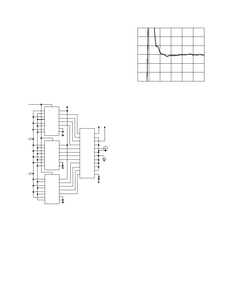
Settling Time Considerations
As can be seen from Table I and the specifications page, the set-
tling time of the AD568 is application dependent. The fastest
settling is achieved in the current-output mode, since the volt-
age output mode requires the output capacitance to be charged
to the appropriate voltage. The DAC's relatively large output
current helps to minimize this effect, but settling-time sensitive
applications should avoid any unnecessary parasitic capacitance
at the output node of voltage output configurations. Direct mea-
surement of the fine scale DAC settling time, even in the voltage
output mode, is extremely tricky: analog scope front ends are
generally incapable of recovering from overdrive quickly enough
to give an accurate settling representation. The plot shown in
Figure 14 was obtained using Data Precision's 640 16-bit sam-
pling head, which features the quick overdrive recovery charac-
teristic of sampling approaches combined with high accuracy
and relatively small thermal tail.
TIME ≠ ns
0
120
20
DAC OUTPUT ≠ VOLTS
40
60
80
100
1.026
1.024
1.022
Figure 14. Zero to Full-Scale Settling
Glitch Considerations
In many high-speed DAC applications, glitch performance is a
critical specification. In a conventional DAC architecture such
as the AD568 there are two basic glitch mechanisms: data skew
and digital feedthrough. A thorough understanding of these
sources can help the user to minimize glitch in any application.
DIGITAL FEEDTHROUGH--As with any converter product,
a high-speed digital-to-analog converter is forced to exist on the
frontier between the noisy environment of high-speed digital
logic and the sensitive analog domain. The problems of this in-
terfacing are particularly acute when demands of high speed
(greater than 10 MHz switching times) and high precision (12
bits or more) are combined. No amount of design effort can
perfectly isolate the analog portions of a DAC from the spectral
components of a digital input signal with a 2 ns risetime. Inevi-
tably, once this digital signal is brought onto the chip, some of
its higher frequency components will find their way to the sensi-
tive analog nodes, producing a digital feedthrough glitch. To
minimize the exposure to this effect, the AD568 has intention-
ally omitted the on-board latches that have been included in
many slower DACs. This not only reduces the overall level of
digital activity on chip, it also avoids bringing a latch clock pulse
on board, whose opposite edge inevitably produces a substantial
glitch, even when the DAC is not supposed to be changing
codes. Another path for digital noise to find its way onto a con-
verter chip is through the reference input pin. The completely
internal reference featured in the AD568 eliminates this noise
input, providing a greater degree of signal integrity in the analog
portions of the chip.
DATA SKEW--The AD568, like many of its slower predeces-
sors, essentially uses each digital input line to switch a separate,
weighted current to either the output (I
OUT
) or some other node
(ANALOG COM). If the input bits are not changed simulta-
neously, or if the different DAC bits switch at different speeds,
then the DAC output current will momentarily take on some in-
correct value. This effect is particularly troublesome at the
"carry points", where the DAC output is to change by only one
LSB, but several of the larger current sources must be switched
to realize this change. Data skew can allow the DAC output to
move a substantial amount towards full scale or zero (depending
upon the direction of the skew) when only a small transition is
desired. Great care was taken in the design and layout of the
AD568 to ensure that switching times of the DAC switches are
symmetrical and that the length of the input data lines are short

AD568
REV. A
≠9≠
and well matched. The glitch-sensitive user should be equally
diligent about minimizing the data skew at the AD568's inputs,
particularly for the 4 or 5 most significant bits. This can be
achieved by using the proper logic family and gate to drive the
DAC, and keeping the interconnect lines between the logic out-
puts and the DAC inputs as short and as well matched as pos-
sible, particularly for the most significant bits. The top 6 bits
should be driven from the same latch chip if latches are used.
Glitch Reduction Schemes
BIT-DESKEWING--Even carefully laid-out boards using the
proper driving logic may suffer from some degree of data-skew
induced glitch. One common approach to reducing this effect is
to add some appropriate capacitance (usually several pF) to
each of the 2 or 3 most significant bits. The exact value of each
capacitor for a given application should be determined experi-
mentally, as it will be dependent on circuit board layout and the
type of driving logic used. Table II presents a few examples of
how the glitch impulse may be reduced through passive
deskewing.
Table II. Bit Delay Glitch Reduction Examples
1
Logic
Uncompensated
Compensation
Compensated
Family
Gate
Glitch
Used
Glitch
HCMOS 74157 350 pV-s
C2 = 5 pF
250 pV-s
STTL
74158 850 pV-s
R1 = 50
,
600 pV-s
C1 = 7 pF
NOTE
1
Measurements were made using a modified version of the fixture shown in
Figure 13, with resistors and capacitors placed as shown in Figure 15. Resis-
tance and capacitance values were set to zero except as noted.
As Figure 15 indicates, in some cases it may prove useful to
place a few hundred ohms of series resistance in the input line
to enhance the delay effect. This approach also helps to reduce
some of the digital feedthrough glitch, as the higher frequency
spectral components are being filtered out of the most signifi-
cant bits' digital inputs.
1
2
3
4
5
6
R1
R2
R3
FROM
DRIVING
LOGIC
BIT 1 (MSB)
BIT 2
BIT 3
BIT 4
BIT 5
BIT 6
AD568
R ≠ C BIT DESKEWING SCHEME
Figure 15. R-C Bit Deskewing Scheme
THRESHOLD SHIFT--It is also possible to reduce the data
skew by shifting the level of logic voltage threshold, V
TH
(Pin
13). This can be readily accomplished by inserting some resis-
tance between the THRESHOLD COM pin (Pin 14) and
ground, as in Figure 16. To generate threshold voltages below
1.4 V, Pin 13 may be directly driven with a voltage source, leav-
ing Pin 14 tied to the ground plane. As Note 2 in Table III indi-
cates, lowering the threshold voltage may reduce output voltage
compliance below the specified limits, which may be of concern
in an unbuffered voltage output topology.
14
13
+5V
RA
RB
THCOM
V
TH
C1
AD568
C1: 1000pF CHIP CAPACITOR
ANALOG
GROUND
PLANE
Figure 16. Positive Threshold Voltage Shift
Table III shows the glitch reduction achieved by shifting the
threshold voltage for HCMOS, STTL, and FAST logic.
Table III. Threshold Shift for Glitch Improvement
1
Logic
Uncompensated Modified
Resulting
Family
Gate
Glitch
Threshold
2
Glitch
HCMOS 74HC158 350 pV-s
1.7 V
150 pV-s
STTL
74S158
850 pV-s
1.0 V
200 pV-s
FAST
74F158
1000 pV-s
1.3 V
480 pV-s
NOTES
1
Measurements made on a modified version of the circuit shown in Figure 13,
with a 1 V full scale.
2
Use care in any scheme that lowers the threshold voltage since the output volt-
age compliance of the DAC is sensitive to this voltage. If the DAC is to be op-
erating in the voltage output mode, it is strongly suggested that the threshold
voltage be set at least 200 mV above the output voltage full scale.
Deglitching
Some applications may prove so sensitive to glitch impulse that
reduction of glitch impulse by an order of magnitude or more is
required. In order to realize glitch impulses this low, some sort
of sample-and-hold amplifier (SHA)-based deglitching scheme
must be used.
There are high-speed SHAs available with specifications suffi-
cient to deglitch the AD568, however most are hybrid in design
at costs which can be prohibitive. A high performance, low cost
alternative shown in Figure 17 is a discrete SHA utilizing a
high-speed monolithic op amp and high-speed DMOS FET
switches.
This SHA circuit uses the inverting integrator architecture. The
AD841 operational amplifier used (300 MHz gain bandwidth
product) is fabricated on the same high-speed process as the
AD568. The time constant formed by the 200
resistor and the
100 pF capacitor determines the acquisition time and also band
limits the output signal to eliminate slew induced distortion.
A discrete drive circuit is used to achieve the best performance
from the SD5000 quad DMOS switch. This switch driving cell
is composed of MPS571 RF npn transistors and an MC10124
TTL to ECL translator. Using this technique provides both
high speed and highly symmetrical drive signals for the SD5000
switches. The switches are arranged in a single-throw double-
pole (SPDT) configuration. The 360 pF "flyback" capacitor is
switched to the op amp summing junction during the hold mode
to keep switching transients from feeding to the output. The ca-
pacitor is grounded during sample mode to minimize its effect
on acquisition time.

AD568
REV. A
≠10≠
Circuit layout for a high speed SHA is almost as critical as the
design itself. Figure 17 shows a recommended layout of the
deglitching cell for a double sided printed circuit board. The
layout is very compact with care taken that all critical signal
paths are short.
≠5V
MC
10124
249
169
510
360
360
≠5V
169
249
500pF
OUTPUT
75
200
200
IN4735
+15V
≠15V
≠15V
20k
1.6
0.39µF
TO PIN 2
SD5000
100pF
4
5
10
11
9
16
14
13
12
6
8
5
4
3
1
AD841
Figure 17. High Performance Deglitcher
Grounding Rules
The AD568 brings out separate reference, output, and digital
power grounds. This allows for optimum management of signal
ground currents for low noise and high-speed-settling perfor-
mance. The separate ground returns are provided to minimize
changes in current flow in the analog signal paths. In this way,
logic return currents are not summed into the same return path
with the analog signals.
It is important to understand which supply and signal currents
are flowing in which grounds so that they may be returned to
the proper power supply in the best possible way.
The majority of the current that flows into the V
CC
supply (Pin
24) flows out (depending on the DAC input code) either the
ANALOG COMMON (Pin 18), the LADDER COMMON
(Pin 17), and/or I
OUT
(Pin 20).
The current in the LADDER COMMON is configured to be
code independent when the output current is being summed
into a virtual ground. If I
OUT
is operated into its own output im-
pedance (or in any unbuffered voltage output mode) the current
in LADDER COMMON will become partially code dependent.
The current in the ANALOG COMMON (Pin 18) is an ap-
proximate complement of the current in I
OUT
, i.e., zero when
the DAC is at full scale and approximately 10 mA at zero input
code.
A relatively constant current (not code dependent) flows out the
REFERENCE COMMON (Pin 23).
The current flowing out of the V
EE
supply (Pin 22) comes from
a combination of reference ground and BIPOLAR OFFSET
(Pin 21). The plus and minus 15 V supplies are decoupled to
the REFERENCE COMMON.
The ground side of the load resistor R
L
, ANALOG COMMON
and LADDER COMMON should be tied together as close to
the package pins as possible. The analog output voltage is then
referred to this node and thus it becomes the "high quality"
ground for the AD568. The REFERENCE COMMON (and
Bipolar offset when not used), should also be connected to this
node.
All of the current that flows into the V
TH
terminal (Pin 13) from
the resistor tied to the 5 V logic supply (or other convenient
positive supply) flows out the THRESHOLD COMMON (Pin
14). This ground pin should be returned directly to the digital
ground plane on its own individual line.
The +5 V logic supply should be decoupled to the THRESH-
OLD COMMON.
Because the V
TH
pin is connected directly to the DAC switches
it should be decoupled to the analog output signal common.
In order to preserve proper operation of the DAC switches, the
digital and analog grounds need to eventually be tied together.
This connection between the ground planes should be made
within 1/2" of the DAC.
The Use of Ground and Power Planes
If used properly, ground planes can perform a myriad of func-
tions on high-speed circuit boards: bypassing, shielding, current
transport, etc. In mixed signal design, the analog and digital por-
tions of the board should be distinct from one another, with the
analog ground plane covering analog signal traces and the digital
ground plane confined to areas covering digital interconnect.
The two ground planes should be connected at or near the
DAC. Care should be taken to insure that the ground plane is
uninterrupted over crucial signal paths. On the digital side, this
includes the digital input lines running to the DAC and any
clock lines. On the analog side, this incudes the DAC output
signal as well as the supply feeders. The use of side runs or
planes in the routing of power lines is also recommended. This
serves the dual function of providing a low series impedance
power supply to the part as well as providing some ``free'' ca-
pacitive decoupling to the appropriate ground plane. Figure
18 illustrates many of the points discussed above. If more layers
of interconnect are available, even better results are possible.
Using the Right Bypass Capacitors
Probably the most important external components associated
with any high-speed design are the capacitors used to bypass
the power supplies. Both selection and placement of these ca-
pacitors can be critical and, to a large extent, dependent upon
the specifics of the system configurations. The dominant consid-
eration in selection of bypass capacitors for the AD568 is mini-
mization of series resistance and inductance. Many capacitors
will begin to look inductive at 20 MHz and above, the very fre-
quencies we are most interested in bypassing. Ceramic and film-
type capacitors generally feature lower series inductance than
tantalum or electrolytic types. A few general rules are of univer-
sal use when approaching the problem of bypassing:
Bypass capacitors should be installed on the printed circuit
board with the shortest possible leads consistent with reliable
construction. This helps to minimize series inductance in the
leads. Chip capacitors are optimal in this respect.
Some series inductance between the DAC supply pins and the
power supply plane often helps to filter out high-frequency
power supply noise. This inductance can be generated using a
small ferrite bead.

AD568
REV. A
≠11≠
5V
DIGITAL GROUND
PLANE
CLOCK
ANALOG GROUND
PLANE
+15V
≠15V
OUTPUT
5V
INPUT
WORDS
AD568
SETTLING/GLITCH
EVALUATION BOARD
Component Side
ANALOG +5V
+5V
ANALOG V
CC
ANALOG V
EE
Foil Side
Figure 18. Printed Circuit Board Layout
High-Speed Interconnect and Routing
It is essential that care be taken in the signal and power ground
circuits to avoid inducing extraneous voltage drops in the signal
ground paths. It is suggested that all connections be short and
direct, and as physically close to the package as possible, so that
the length of any conduction path shared by external compo-
nents will be minimized. When runs exceed an inch or so in
length, some type of termination resistor may be required. The
necessity and value of this resistor will be dependent upon the
logic family used.
For maximum ac performance, the DAC should be mounted di-
rectly to the circuit board; sockets should not be used as they in-
troduce unwanted capacitive coupling between adjacent pins of
the device.
Applications
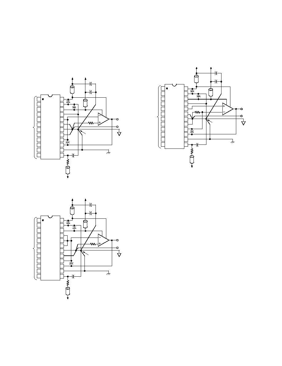
1 s, 12-BIT SUCCESSIVE APPROXIMATION A/D
CONVERTER
The AD568's unique combination of high speed and true 12-bit
accuracy can be used to construct a 12-bit SAR-type A/D con-
verter with a sub-
µ
s conversion time. Figure 19 shows the con-
figuration used for this application. A negative analog input
voltage is converted into current and brought into a summing
junction with the DAC current. This summing junction is
bidirectionally clamped with two Schottky diodes to limit its
voltage excursion from ground. This voltage is differentially am-
plified and passed to a high-speed comparator. The comparator
output is latched and fed back to the successive approximation
register, which is then clocked to generated the next set of codes
for the DAC.
13
16
15
14
24
23
22
21
20
19
18
17
+15V
REFCOM
≠15V
I
BPO
R
L
ACOM
LCOM
SPAN
SPAN
THCOM
V
TH
I
OUT
12
11
10
9
8
1
2
3
4
7
6
5
DAC
AD568
0.2µF
0.1µF
0.1µF
0.1µF
≠15V
+15V
ANALOG
GND PLANE
100pF
1k
+5V
NC
NC
4
7
6
5
21
20
19
18
17
16
9
8
Q11
Q10
Q9
Q8
Q6
Q5
Q4
Q3
Q2
Q1
Q0
Q7
11
3
14
1
13
24
12
2
23
22
15
10
V
CC
GND
D0
Q
11
NC
NC
CP
E
S
CC
D
NC
+5V
PARALLEL DATA
OUT
SAR
2504
0.01µF
1k
620
620
2.5k
V
I
0 TO ≠10.24V
N
+5V
≠5V
≠5V
1k
150
Q1
Q2
Q3
D1
D2
27k
≠15V
1
2
3
4
8
7
6
5
V+
+IN
V≠
≠IN
OUT
OUT
LCH
GND
COMPARATOR
LT1016
D3
IN4148
CONVERSION COMPLETE
START COMVERT
CHIP ENABLE
150k
+5V
INVERTER
74HC04
15k
150k
Q4
Q5
Figure 19. AD568 1
µ
s Successive Approximation A/D Application

AD568
REV. A
≠12≠
Circuit Details
Figure 20 shows an approximate timing budget for the A/D con-
verter. If 12 cycles are to be completed in 1
µ
s, approximately
80 ns is allowed for each cycle. Since the Schottky diodes clamp
the voltage of the summing junction, the DAC settling time ap-
proaches the current-settling value of 35 ns, and hence uses up
less than half the timing budget.
To maintain simplicity, a simple clock is used that runs at a
constant rate throughout the conversion, with a duty cycle of
approximately 90%. If absolute speed is worth the additional
complexity, the clock frequency can be increased as the conver-
sion progresses since the DAC must settle from increasingly
smaller steps.
When seeking a cycle time of less than 100 ns, the delays gener-
ated by the older generation SAR registers become problematic.
Newer, high speed SAR logic chips are becoming available in
the classic 2504 pinout that cuts the logic overhead in half. One
example of this is Zyrel's ZR2504.
Finding a comparator capable of keeping up with this DAC ar-
rangement is fairly difficult: it must respond to an overdrive of
250
µ
V (1 LSB) in less than 25 ns. Since no inexpensive com-
parator exists with these specs, special arrangements must be
made. The LT106 comparator provides relatively quick re-
sponse, but requires at least 5 mV of overdrive to maintain this
speed. A discrete preamplifier may be used to amplify the sum-
ming junction voltage to sufficiently overdrive the comparator.
Care must be exercised in the layout of the preamp/comparator
block to avoid introducing comparator instability with the
preamp's additional gain.
10ns
35ns
15ns
10ns
10ns
0
10ns
20ns
30ns
40ns
50ns
60ns
70ns
80ns
CLOCK
PULSE
START OF NEXT
CLOCK CYCLE
LATCH COMPARATOR
START OF
CLOCK CYCLE
SAR
DELAY
DAC SETTLING
PREAMP
DELAY
COMPARATOR
DELAY
Figure 20. Typical Clock Cycle for a 1
µ
s SAR A/D
Converter
HIGH-SPEED MULTIPLYING DAC
A powerful use for the AD568 is found in multiplying applica-
tions, where the DAC controls the amplitude of a high-speed
signal. Specifically, using the AD568 as the control voltage
input signal for the AD539 60 MHz analog multiplier and
AD5539 wideband op amp, a high-speed multiplying DAC can
be built.
In the application shown in Figure 21, the AD568 is used in a
buffered voltage output mode to generate the input to the
AD539's control channel. The speed of the AD568 allows
oversampling of the control signal waveform voltage, thereby
providing increased spectral purity of the amplitude envelope
that modulates the analog input channels.
The AD568 is configured in the unbuffered unipolar output
mode. The internal 200
load resistor creates the 0-1 V FS
output signal, which is buffered and amplified to a 0-3 V range
suitable for the control channel of the AD539.
A 500
input impedance exists at Pin 1, the input channel. To
provide a buffer for the 0-1 V output signal from the AD568
looking into the impedance and to achieve the full-scale range,
the AD841, high-speed, fast settling op amp is included. The
gain of 3 is achieved with a 2 k
resistor configured in follower
mode with a 1 k
pot and 500
resistor. A 20 k
pot with
connections to Pins 3, 4 and 12 is provided for offset trim.
The AD539 can accept two separate input signals, each with a
nominal full-scale voltage range of
±
2 V. Each signal can then
be simultaneously controlled by the AD568 signal at the com-
mon input channels, Pins 11 and 14, applied to the AD5539 in
a subtracting configuration, provide the voltage output signal:
V
OUT
=
D
4096
◊
V
Y1
≠V
Y 2
2V
(0
D
4095)
For applications where only a single channel is involved, chan-
nel 2, V
Y2
, is tied to ground. This provides:
V
OUT
=
D
4096
◊
V
Y1
2V
(0
D
4095)
Some AD539 circuit details: The control amplifier compensa-
tion capacitor for Pin 2, C
C
, must have a minimum value of
300 pF to provide circuit stability. For improved bandwidth and
feedthrough, the feedthrough capacitor between Pins 1 and 2
should be 5-20% of C
C
. A Schottky diode at Pin 2 can improve
recovery time from small negative values of V
X
. Lead lengths
along the path of the high-speed signal from AD568 should be
kept at a minimum.

AD568
REV. A
≠13≠
16
15
13
16
15
14
24
23
22
21
20
19
18
17
12
11
10
9
8
1
2
3
4
7
6
5
AD568
+15V
REFCOM
≠15V
I
BPO
R
L
ACOM
LCOM
SPAN
SPAN
THCOM
VTH
I
OUT
DIGITAL
INPUTS
0.2µF
0.1µF
0.1µF
0.1µF
≠15V
+15V
ANALOG
GND PLANE
DIGITAL
GND PLANE
DIGITAL
SUPPLY
GROUND
100pF
R
TH
1k
+5V
NC
NC
ANALOG
OUTPUT
ANALOG
SUPPLY
GROUND
4
3
10
12
6
5
C
ff
100pF
C
c
3000pF
75
1µF
1µF
≠V
S
20k
AD841
2k
1k
500
+V
S
13
14
1
2
3
4
5
6
7
8
9
10
11
12
AD568
W1
Z1
CH1
OUTPUT
BASE
COMMON
Z2
W2
CH2
OUTPUT
11
+V
S
≠V
S
CONTROL
HF
COMP
CH1
INPUT
INPUT
COMMON
OUTPUT
COMMON
CH2
INPUT
V
X
75
V
Y1
IN
V
Y1
IN
10
10
+9V
≠9V
200
GAIN
ADJUST
(
±
4% RANGE)
10
7
1
14
≠9V
AD5539N
8
100k
180
470
2.7
0.47µF
≠9V
50k
(OPTIONAL)
OUTPUT
OFFSET
≠9V
+9V
+9V
0.47µF
2.7
V
OUT
3
D1
180
C
F
0.25pF ≠
1.5pF
D1: THOMPSON CSFBAR ≠ 10 OR SIMILAR SCHOTTKY DIODE
SHORT, DIRECT CONNECTION TO GROUND PLANE.
Figure 21. Wideband Digitally Controlled Multiplier
OUTLINE DIMENSIONS
Dimensions shown in inches and (mm).
24-Pin Cerdip (Suffix Q)

C1014a≠9≠7/87
PRINTED IN U.S.A.
≠14≠