 | ÐлекÑÑоннÑй компоненÑ: AD588TQ | СкаÑаÑÑ:  PDF PDF  ZIP ZIP |
Äîêóìåíòàöèÿ è îïèñàíèÿ www.docs.chipfind.ru
REV. D
Information furnished by Analog Devices is believed to be accurate and
reliable. However, no responsibility is assumed by Analog Devices for its
use, nor for any infringements of patents or other rights of third parties that
may result from its use. No license is granted by implication or otherwise
under any patent or patent rights of Analog Devices. Trademarks and
registered trademarks are the property of their respective companies.
One Technology Way, P.O. Box 9106, Norwood, MA 02062-9106, U.S.A.
Tel: 781/329-4700
www.analog.com
Fax: 781/326-8703
© 2003, Analog Devices, Inc. All rights reserved.
AD588
*
High Precision Voltage Reference
FEATURES
Low Drift: 1.5 ppm/ C
Low Initial Error: 1 mV
Pin Programmable Output:
+10 V, +5 V, +65 V Tracking, 5 V, 10 V
Flexible Output Force and Sense Terminals
High Impedance Ground Sense
Machine lnsertable DIP Packaging
MIL-STD-883 Compliant Versions Available
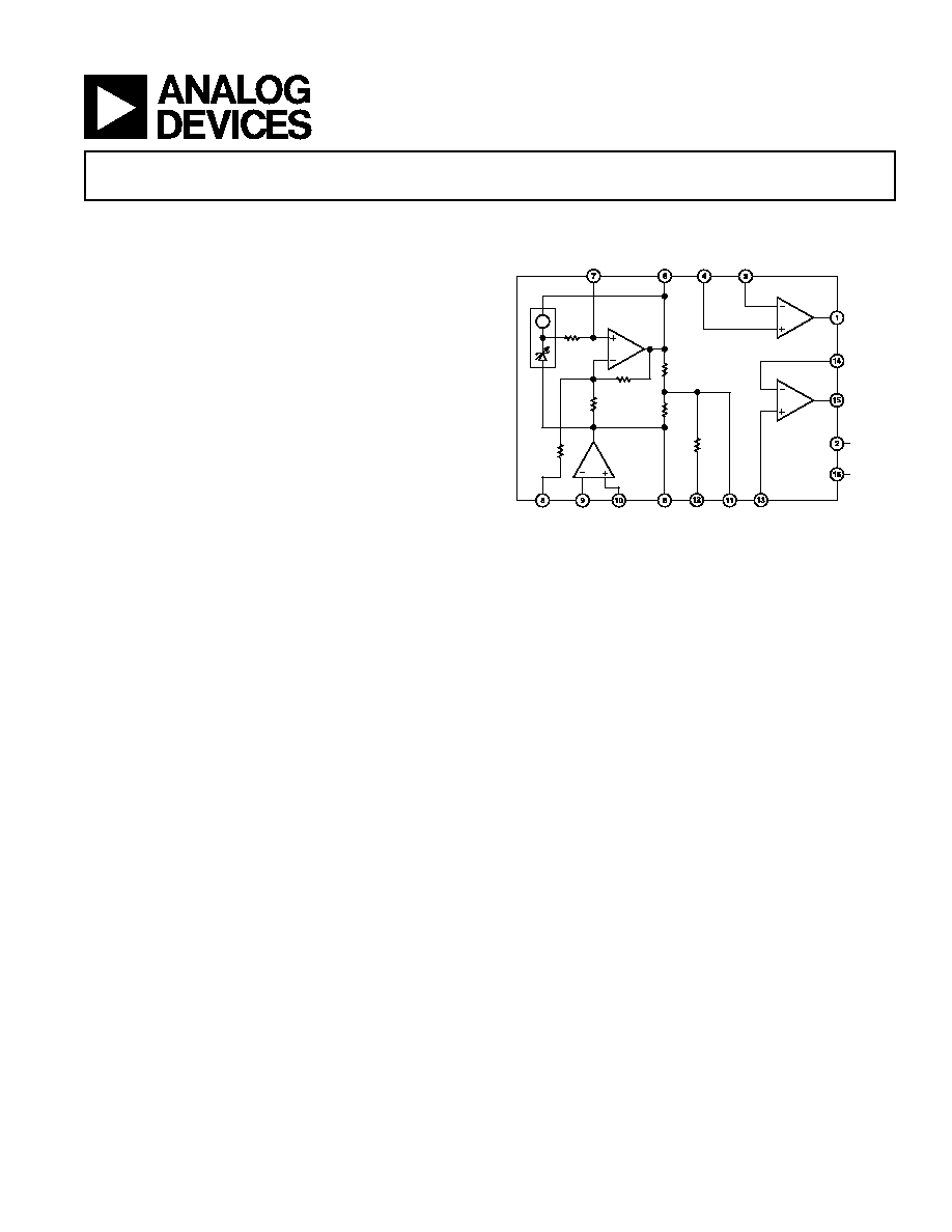
FUNCTIONAL BLOCK DIAGRAM
R3
R
B
R1
R2
R4
R5
R6
GAIN
ADJ
GND
SENSE
+IN
GND
SENSE
IN
V
LOW
BAL
ADJ
V
CT
A4 IN
V
S
+V
S
A4 OUT
FORCE
A4 OUT
SENSE
A3 OUT
FORCE
A3 OUT
SENSE
A3 IN
V
HIGH
NOISE
REDUCTION
A1
A4
AD588
A3
A2
GENERAL DESCRIPTION
The AD588 represents a major advance in the state-of-the-art
in monolithic voltage references. Low initial error and low tem-
perature drift give the AD588 absolute accuracy performance
previously not available in monolithic form. The AD588 uses a
proprietary ion-implanted buried Zener diode, and laser-wafer-
drift trimming of high stability thin-film resistors to provide
outstanding performance at low cost.
The AD588 includes the basic reference cell and three additional
amplifiers that provide pin programmable output ranges. The
amplifiers are laser-trimmed for low offset and low drift to main-
tain the accuracy of the reference. The amplifiers are configured
to allow Kelvin connections to the load and/or boosters for driv-
ing long lines or high current loads, delivering the full accuracy
of the AD588 where it is required in the application circuit.
The low initial error allows the AD588 to be used as a system
reference in precision measurement applications requiring 12-bit
absolute accuracy. In such systems, the AD588 can provide a
known voltage for system calibration in software, and the low
drift allows compensation for the drift of other components in
a system. Manual system calibration and the cost of periodic
recalibration can therefore be eliminated. Furthermore, the
mechanical instability of a trimming potentiometer and the
potential for improper calibration can be eliminated by using
the AD588 in conjunction with autocalibration software.
The AD588 is available in four versions. The AD588JQ and
AD588KQ and grades are packaged in a 16-lead CERDIP and
are specified for 0
°C to 70°C operation. AD588AQ and BQ
grades are packaged in a 16-lead CERDIP and are specified for
the 25
°C to +85°C industrial temperature range.
*Protected by Patent Number 4,644,253.
PRODUCT HIGHLIGHTS
1. The AD588 offers 12-bit absolute accuracy without any user
adjustments. Optional fine-trim connections are provided for
applications requiring higher precision. The fine trimming does
not alter the operating conditions of the Zener or the buffer
amplifiers, and thus does not increase the temperature drift.
2. Output noise of the AD588 is very low--typically 6
µV p-p.
A pin is provided for additional noise filtering using an exter-
nal capacitor.
3. A precision
±5 V tracking mode with Kelvin output connec-
tions is available with no external components. Tracking error
is less than 1 mV and a fine-trim is available for applications
requiring exact symmetry between the +5 V and 5 V outputs.
4. Pin strapping capability allows configuration of a wide vari-
ety of outputs:
± 5 V, +5 V, +10 V, 5 V, and 10 V dual
outputs or +5 V, 5 V, +10 V, and 10 V single outputs.

REV. D
2
AD588SPECIFICATIONS
(Typical @ 25
°
C, 10 V output, V
S
= 15 V, unless otherwise noted.
1
)
AD588JQ/AQ
AD588BQ/KQ
Parameter
Min
Typ
Max
Min
Typ
Max
Unit
OUTPUT VOLTAGE ERROR
+10 V, 10 V Outputs
±3
1
+1
mV
+5 V, 5 V Outputs
±3
1
+1
mV
±5 V TRACKING MODE
Symmetry Error
±1.5
±0.75
mV
OUTPUT VOLTAGE DRIFT
0
°C to 70°C (J, K, B)
±2
±3
±1.5
ppm/
°C
25
°C to +85°C (A, B)
±3
±3
ppm/
°C
GAIN ADJ AND BAL ADJ
2
Trim Range
±4
±4
mV
Input Resistance
150
150
k
LINE REGULATION
T
MIN
to T
MAX
3
±200
±200
µV/V
LOAD REGULATION
T
MIN
to T
MAX
+10 V Output, 0 mA < I
OUT
< 10 mA
±50
±50
µV/mA
10 V Output, 10 mA < I
OUT
< 0 mA
±50
±50
µV/mA
SUPPLY CURRENT
T
MIN
to T
MAX
6
10
6
10
mA
Power Dissipation
180
300
180
300
mW
OUTPUT NOISE (Any Output)
0.1 Hz to 10 Hz
6
6
µV p-p
Spectral Density, 100 Hz
100
100
nV/
Hz
LONG-TERM STABILITY (@ 25
°C)
15
15
ppm/1000 hr
BUFFER AMPLIFIERS
Offset Voltage
100
10
µV
Offset Voltage Drift
1
1
µV/°C
Bias Current
20
20
nA
Open-Loop Gain
110
110
dB
Output Current A3, A4
10
+10
10
+10
mA
Common-Mode Rejection (A3, A4)
V
CM
= 1 V p-p
100
100
dB
Short Circuit Current
50
50
mA
TEMPERATURE RANGE
Specified Performance
J, K Grades
0
70
0
70
°C
A, B Grades
25
+85
25
+85
°C
NOTES
1
Output
Configuration
+10 V
Figure 2a
10 V
Figure 2c
+5 V, 5 V,
± 5 V
Figure 2b
Specifications tested using +10 V configuration, unless otherwise indicated.
2
Gain and balance adjustments guaranteed capable of trimming output voltage error and symmetry error to zero.
3
Test Conditions:
+10 V Output
V
S
= 15 V, 13.5 V
+V
S
18 V
10 V Output
18 V
V
S
13.5 V, +V
S
= 15 V
±5 V Output
+V
S
= +18 V, V
S
= 18 V
+V
S
= +10.8 V, V
S
= 10.8 V
For
±10 V output, ±V
S
can be as low as
±12 V.
Specifications subject to change without notice.
Specifications shown in boldface are tested on all production units at final electrical test. Results from those tests are used to calculate outgoing quality
levels. All min and max specifications are guaranteed, although only those shown in boldface are tested on all production units.
REV. D
AD588
3
CAUTION
ESD (electrostatic discharge) sensitive device. Electrostatic charges as high as 4000 V readily
accumulate on the human body and test equipment and can discharge without detection. Although the
AD588 features proprietary ESD protection circuitry, permanent damage may occur on devices
subjected to high energy electrostatic discharges. Therefore, proper ESD precautions are recommended
to avoid performance degradation or loss of functionality.
ORDERING GUIDE
Part Number
1
Initial Error (mV)
Temperature Coefficient
2
Temperature Range (
°C)
Package Option
AD588AQ
3
3 ppm/
°C
25 to +85
CERDIP (Q-16)
AD588BQ
1
1.5 ppm/
°C
25 to +85
2
CERDIP (Q-16)
AD588JQ
3
3 ppm/
°C
0 to 70
CERDIP (Q-16)
AD588KQ
1
1.5 ppm/
°C
0 to 70
CERDIP (Q-16)
NOTES
1
For details on grade and package offerings screened in accordance with MIL-STD-883, refer to the Analog Devices Military Products Databook or current
AD588/883B.
2
Temperature coefficient specified from 0
°C to 70°C.
ABSOLUTE MAXIMUM RATINGS
*
+V
S
to V
S
. . . . . . . . . . . . . . . . . . . . . . . . . . . . . . . . . . . . . 36 V
Power Dissipation (25
°C) . . . . . . . . . . . . . . . . . . . . . . 600 mW
Storage Temperature Range . . . . . . . . . . . . . 65
°C to +150°C
Lead Temperature Range (Soldering 10 sec) . . . . . . . . . 300
°C
Package Thermal Resistance (
JA
/
JC
) . . . . . . . . 90
°C/25°C/W
Output Protection: All Outputs Safe if Shorted to Ground
*Stresses above those listed under Absolute Maximum Ratings may cause perma-
nent damage to the device. This is a stress rating only; functional operation of the
device at these or any other conditions above those indicated in the operational
sections of this specification is not implied. Exposure to absolute maximum rating
conditions for extended periods may affect device reliability.
TOP VIEW
(Not to Scale)
16
15
14
13
12
11
10
9
1
2
3
4
5
6
7
8
A3 OUT FORCE
+V
S
A3 OUT SENSE
A3 IN
GAIN ADJ
V
HIGH
NOISE
REDUCTION
V
LOW
V
S
A4 OUT FORCE
A4 OUT SENSE
A4 IN
BAL ADJ
V
CT
GND SENSE IN
GND SENSE +IN
AD588
PIN CONFIGURATION
REV. D
4
AD588
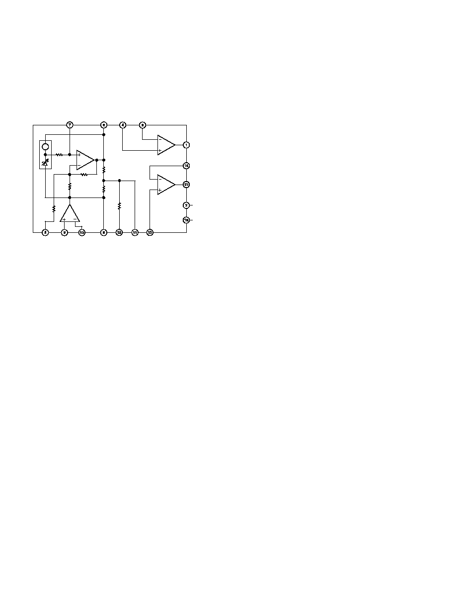
THEORY OF OPERATION
The AD588 consists of a buried Zener diode reference, amplifiers
used to provide pin programmable output ranges, and associ-
ated thin-film resistors as shown in Figure 1. The temperature
compensation circuitry provides the device with a temperature
coefficient of 1.5 ppm/
°C or less.
R3
R
B
R1
R2
R4
R5
R6
GAIN
ADJ
GND
SENSE
+IN
GND
SENSE
IN
V
LOW
BAL
ADJ
V
CT
A4 IN
V
S
+V
S
A4 OUT
FORCE
A4 OUT
SENSE
A3 OUT
FORCE
A3 OUT
SENSE
A3 IN
V
HIGH
NOISE
REDUCTION
A1
A4
AD588
A3
A2
Figure 1. AD588 Functional Block Diagram
Amplifier A1 performs several functions. A1 primarily acts to
amplify the Zener voltage from 6.5 V to the required 10 V output.
In addition, A1 also provides for external adjustment of the
10 V output through Pin 5, GAIN ADJ. Using the bias compen-
sation resistor between the Zener output and the noninverting
input to A1, a capacitor can be added at the NOISE REDUCTION
pin (Pin 7) to form a low-pass filter and reduce the noise contri-
bution of the Zener to the circuit. Two matched 10 k
nominal
thin-film resistors (R4 and R5) divide the 10 V output in half.
Pin V
CT
(Pin 11) provides access to the center of the voltage
span and Pin 12 (BAL ADJ) can be used for fine adjustment
of this division.
Ground sensing for the circuit is provided by amplifier A2. The
noninverting input (Pin 9) senses the system ground, which
will be transferred to the point on the circuit where the invert-
ing input (Pin 10) is connected. This may be Pin 6, 8, or 11.
The output of A2 drives Pin 8 to the appropriate voltage. Thus, if
Pin 10 is connected to Pin 8, the V
LOW
pin will be the same
voltage as the system ground. Alternatively, if Pin 10 is con-
nected to the V
CT
pin, it will be ground and Pin 6 and Pin 8 will
be +5 V and 5 V, respectively.
Amplifiers A3 and A4 are internally compensated and are used
to buffer the voltages at Pins 6, 8, and 11, as well as to provide a
full Kelvin output. Thus, the AD588 has a full Kelvin capability
by providing the means to sense a system ground and provide
forced and sensed outputs referenced to that ground.
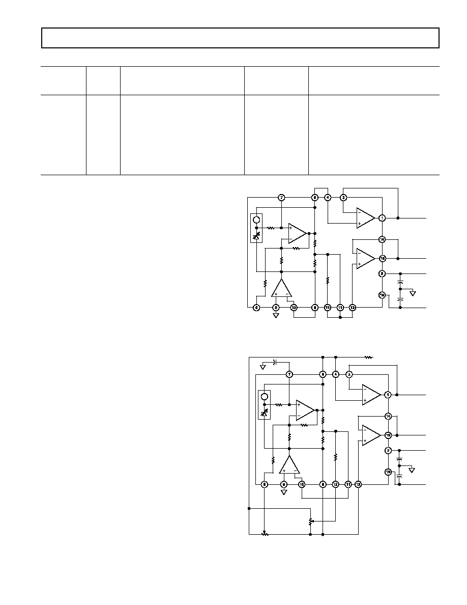
APPLYING THE AD588
The AD588 can be configured to provide +10 V and 10 V
reference outputs as shown in Figures 2a and 2c, respectively. It
can also be used to provide +5 V, 5 V, or a
± 5 V tracking
reference, as shown in Figure 2b. Table I details the appropriate
pin connections for each output range. In each case, Pin 9 is
connected to system ground and power is applied to Pins 2 and 16.
The architecture of the AD588 provides ground sense and
uncommitted output buffer amplifiers that offer the user a great
deal of functional flexibility. The AD588 is specified and tested
in the configurations shown in Figure 2a. The user may choose
to take advantage of the many other configuration options available
with the AD588. However, performance in these configurations
is not guaranteed to meet the extremely stringent data sheet
specifications.
As indicated in Table I, a +5 V buffered output can be provided
using amplifier A4 in the +10 V configuration (Figure 2a). A 5 V
buffered output can be provided using amplifier A3 in the 10 V
configuration (Figure 2c). Specifications are not guaranteed for
the +5 V or 5 V outputs in these configurations. Performance
will be similar to that specified for the +10 V or 10 V outputs.
As indicated in Table I, unbuffered outputs are available at
Pins 6, 8, and 11. Loading of these unbuffered outputs will
impair circuit performance.
Amplifiers A3 and A4 can be used interchangeably. However,
the AD588 is tested (and the specifications are guaranteed) with
the amplifiers connected as indicated in Figure 2a and Table I.
When either A3 or A4 is unused, its output force and sense pins
should be connected and the input tied to ground.
Two outputs of the same voltage may be obtained by connect-
ing both A3 and A4 to the appropriate unbuffered output on
Pins 6, 8, or 11. Performance in these dual-output configura-
tions will typically meet data sheet specifications.
CALIBRATION
Generally, the AD588 will meet the requirements of a precision
system without additional adjustment. Initial output voltage
error of 1 mV and output noise specs of 10
µV p-p allow for
accuracies of 12 bits to 16 bits. However, in applications where
an even greater level of accuracy is required, additional calibra-
tion may be called for. Provision for trimming has been made
through the use of the GAIN ADJ and BAL ADJ pins (Pins 5 and
12, respectively).
The AD588 provides a precision 10 V span with a center tap
(V
CT
) that is used with the buffer and ground sense amplifiers to
achieve the voltage output configurations in Table I. GAIN
ADJUST and BALANCE ADJUST can be used in any of these
configurations to trim the magnitude of the span voltage and
the position of the center tap within the span. The GAIN
ADJUST should be performed first. Although the trims are not
interactive within the device, the GAIN trim will move the
BALANCE trim point as it changes the magnitude of the span.
REV. D
AD588
5
Figure 2b shows GAIN and BALANCE trims in a +5 V and
5 V tracking configuration. A 100 k
20-turn potentiometer is
used for each trim. The potentiometer for GAIN trim is con-
nected between Pin 6 (V
HIGH
) and Pin 8 (V
LOW
) with the wiper
connected to Pin 5 (GAIN ADJ). The potentiometer is adjusted
to produce exactly 10 V between Pin 1 and Pin 15, the amplifier
outputs. The BALANCE potentiometer, also connected between
Pin 6 and Pin 8 with the wiper to Pin 12 (BAL ADJ), is then
adjusted to center the span from +5 V to 5 V.
Trimming in other configurations works in exactly the same
manner. When producing +10 V and +5 V, GAIN ADJ is used
to trim +10 V and BAL ADJ is used to trim +5 V. In the 10 V
and 5 V configuration, GAIN ADJ is again used to trim the
magnitude of the span, 10 V, while BAL ADJ is used to trim
the center tap, 5 V.
In single output configurations, GAIN ADJ is used to trim outputs
utilizing the full span (+10 V or 10 V), while BAL ADJ is used
to trim outputs using half the span (+5 V or 5 V).
Input impedance on both the GAIN ADJ and BAL ADJ pins is
approximately 150 k
. The GAIN ADJUST trim network
effectively attenuates the 10 V across the trim potentiometer
by a factor of about 1500 to provide a trim range of 3.5 mV to
+7.5 mV with a resolution of approximately 550
µV/turn
(20-turn potentiometer). The BAL ADJ trim network attenu-
ates the trim voltage by a factor of about 1400, providing a
trim range of
±4.5 mV with resolution of 450 µV/turn.
R3
R
B
R1
R2
R4
R5
R6
V
S
+V
S
A1
A4
AD588
A3
A2
SYSTEM
GROUND
+10V
+15V
+5V
15V
SYSTEM
GROUND
0.1 F
0.1 F
Figure 2a. +10 V Output
R3
R
B
R1
R2
R4
R5
R6
V
S
+V
S
A1
A4
AD588
A3
A2
SYSTEM
GROUND
+5V
15V
5V
15V
SYSTEM
GROUND
0.1 F
0.1 F
100k
20T
BALANCE
ADJUST
100k
20T
GAIN ADJUST
+15V
NOISE
REDUCTION
1 F
Figure 2b. +5 V and 5 V Outputs
Table I. Pin Connections
Connect
Buffered
Pin 10
Unbuffered
* Output on Pins
Output
Buffered Output on Pins
Range
to Pin:
10 V
5 V
0 V
+5 V
+10 V
Connections
10 V
5 V
0 V
+5 V
+10 V
+10 V
8
8
11
6
11 to 13, 14 to 15
15
6 to 4, and 3 to 1
1
5 V or +5 V
11
8
11
6
8 to 13, 14 to 15,
15
6 to 4, and 3 to 1
1
10 V
6
8
11
6
8 to 13, 14 to 15,
15
11 to 4, and 3 to 1 1
+5 V
11
6
6 to 4 and 3 to 1
1
5 V
11
8
8 to 13 and 14 to 15
15
*Unbuffered outputs should not be loaded.
Document Outline
- FEATURES
- GENERAL DESCRIPTION
- FUNCTIONAL BLOCK DIAGRAM
- PRODUCT HIGHLIGHTS
- SPECIFICATIONS
- ABSOLUTE MAXIMUM RATINGS
- PIN CONFIGURATION
- ORDERING GUIDE
- THEORY OF OPERATION
- APPLYING THE AD588
- CALIBRATION
- NOISE PERFORMANCE AND REDUCTION
- TURN-ON TIME
- TEMPERATURE PERFORMANCE
- KELVIN CONNECTIONS
- DYNAMIC PERFORMANCE
- USING THE AD588 WITH CONVERTERS
- 14-Bit Digital-to-Analog ConverterAD7535
- 16-Bit Digital-to-Analog ConverterAD569
- SUBSTITUTING FOR INTERNAL REFERENCES
- 12-Bit Analog-to-Digital ConverterAD574A
- RTD EXCITATION
- BOOSTED PRECISION CURRENT SOURCE
- BRIDGE DRIVER CIRCUITS
- OUTLINE DIMENSIONS
- Revision History