 | ÐлекÑÑоннÑй компоненÑ: AD590JR | СкаÑаÑÑ:  PDF PDF  ZIP ZIP |
Äîêóìåíòàöèÿ è îïèñàíèÿ www.docs.chipfind.ru

Two-Terminal IC
Temperature Transducer
AD590
Rev. C
Information furnished by Analog Devices is believed to be accurate and reliable.
However, no responsibility is assumed by Analog Devices for its use, nor for any
infringements of patents or other rights of third parties that may result from its use.
Specifications subject to change without notice. No license is granted by implication
or otherwise under any patent or patent rights of Analog Devices. Trademarks and
registered trademarks are the property of their respective owners.
One Technology Way, P.O. Box 9106, Norwood, MA 02062-9106, U.S.A.
Tel: 781.329.4700
www.analog.com
Fax: 781.326.8703
© 2003 Analog Devices, Inc. All rights reserved.
FEATURES
Linear current output: 1 µA/K
Wide temperature range: -55°C to +150°C
Probe compatible ceramic sensor package
2-terminal device: voltage in/current out
Laser trimmed to ±0.5°C calibration accuracy (AD590M)
Excellent linearity: ±0.3°C over full range (AD590M)
Wide power supply range: 4 V to 30 V
Sensor isolation from case
Low cost
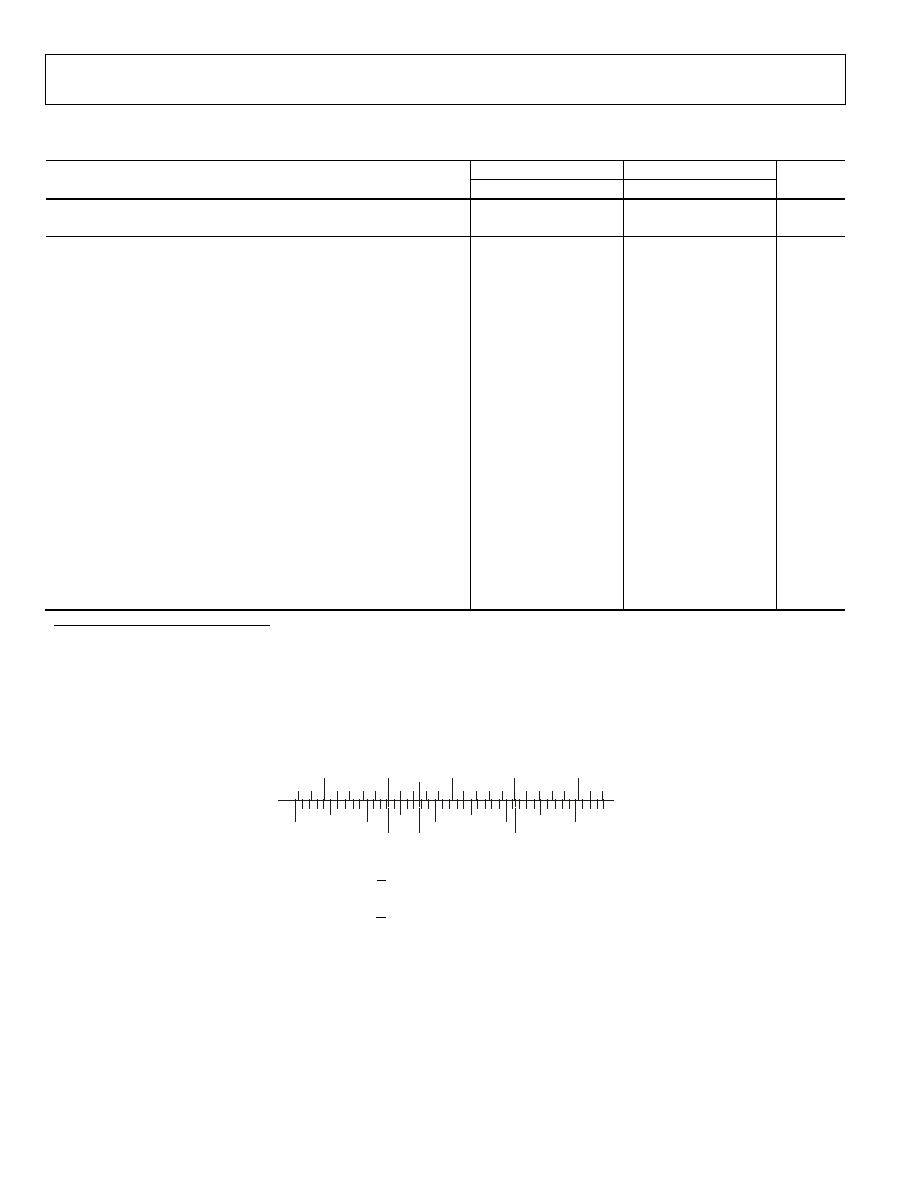
00533-C-001
+
TO-52
SOIC-8
NC = NO CONNECT
TOP VIEW
(Not to Scale)
NC
1
V+
2
V
3
NC
4
NC
NC
NC
NC
8
7
6
5
FLATPACK
+
Figure 1. Pin Designations
GENERAL DESCRIPTION
The AD590 is a 2-terminal integrated circuit temperature
transducer that produces an output current proportional to
absolute temperature. For supply voltages between 4 V and 30 V
the device acts as a high-impedance, constant current regulator
passing 1 µA/K. Laser trimming of the chip's thin-film resistors
is used to calibrate the device to 298.2 µA output at 298.2 K
(25°C).
The AD590 should be used in any temperature-sensing
application below 150°C in which conventional electrical
temperature sensors are currently employed. The inherent low
cost of a monolithic integrated circuit combined with the
elimination of support circuitry makes the AD590 an attractive
alternative for many temperature measurement situations.
Linearization circuitry, precision voltage amplifiers, resistance
measuring circuitry, and cold junction compensation are not
needed in applying the AD590.
In addition to temperature measurement, applications include
temperature compensation or correction of discrete
components, biasing proportional to absolute temperature, flow
rate measurement, level detection of fluids and anemometry.
The AD590 is available in chip form, making it suitable for
hybrid circuits and fast temperature measurements in protected
environments.
The AD590 is particularly useful in remote sensing applications.
The device is insensitive to voltage drops over long lines due to
its high impedance current output. Any well-insulated twisted
pair is sufficient for operation at hundreds of feet from the
receiving circuitry. The output characteristics also make the
AD590 easy to multiplex: the current can be switched by a
CMOS multiplexer or the supply voltage can be switched by a
logic gate output.
PRODUCT HIGHLIGHTS
1. The AD590 is a calibrated, 2-terminal temperature sensor
requiring only a dc voltage supply (4 V to 30 V). Costly
transmitters, filters, lead wire compensation, and
linearization circuits are all unnecessary in applying the
device.
2. State-of-the-art laser trimming at the wafer level in
conjunction with extensive final testing ensures that
AD590 units are easily interchangeable.
3. Superior interface rejection occurs, because the output is a
current rather than a voltage. In addition, power
requirements are low (1.5 mWs @ 5 V @ 25°C). These
features make the AD590 easy to apply as a remote sensor.
4. The high output impedance (>10 M) provides excellent
rejection of supply voltage drift and ripple. For instance,
changing the power supply from 5 V to 10 V results in only
a 1 µA maximum current change, or 1°C equivalent error.
5. The AD590 is electrically durable: it withstands a forward
voltage of up to 44 V and a reverse voltage of 20 V.
Therefore, supply irregularities or pin reversal does not
damage the device.

AD590
Rev. C | Page 2 of 16
TABLE OF CONTENTS
Specifications..................................................................................... 3
AD590J and AD590K Specifications ......................................... 3
AD590L and AD590M Specifications........................................ 4
Absolute Maximum Ratings............................................................ 5
ESD Caution.................................................................................. 5
Product Description......................................................................... 6
Circuit Description....................................................................... 6
Explanation of Temperature Sensor Specifications ................. 6
Calibration Error .......................................................................... 7
Error Versus Temperature: with Calibration Error Trimmed
Out...................................................................................................7
Error Versus Temperature: No User Trims ................................7
Nonlinearity ...................................................................................7
Voltage and Thermal Environment Effects ...............................8
General Applications...................................................................... 10
Outline Dimensions ....................................................................... 13
Ordering Guide .......................................................................... 14
REVISION HISTORY
Revision C
9/03--Data Sheet Changed from REV. B to REV. C.
Added SOIC-8 package..............................Universal
Change to Figure 1..............................................1
Updated OUTLINE DIMENSIONS.........................13
Added ORDERING GUIDE..................................14

AD590
Rev. C | Page 3 of 16
SPECIFICATIONS
AD590J AND AD590K SPECIFICATIONS
Table 1. @ 25°C and V
S
= 5 V unless otherwise noted
AD590J AD590K
Parameter
Min Typ Max Min Typ Max Unit
POWER SUPPLY
Operating Voltage Range
4
30
4
30
Volts
OUTPUT
Nominal Current Output @ 25°C (298.2K)
298.2
298.2
µA
Nominal
Temperature
Coefficient
1
1
µA/K
Calibration Error @ 25°C
±5.0
±2.5
°C
Absolute Error (over rated performance temperature range)
Without External Calibration Adjustment
±10
±5.5
°C
With 25°C Calibration Error Set to Zero
±3.0
±2.0
°C
Nonlinearity
For TO-52 and Flatpack packages
±1.5
±0.8
°C
For 8-Lead SOIC package
±1.5
±1.0
°C
Repeatability
1
±0.1
±0.1
°C
Long-Term Drift
2
±0.1
±0.1
°C
Current
Noise
40
40
pA/
Hz
Power Supply Rejection
4 V
V
S
5 V
0.5
0.5
µA/V
5 V
V
S
15 V
0.2
0.2
µV/V
15 V
V
S
30 V
0.1
0.1
µA/V
Case Isolation to Either Lead
10
10
10
10
Effective
Shunt
Capacitance
100
100
pF
Electrical
Turn-On
Time
20
20
µs
Reverse Bias Leakage Current
3
(Reverse
Voltage
=
10
V)
10
10
pA
1
Maximum deviation between +25°C readings after temperature cycling between 55°C and +150°C; guaranteed, not tested.
2
Conditions: constant 5 V, constant 125°C; guaranteed, not tested.
3
Leakage current doubles every 10°C.
Specifications shown in boldface are tested on all production units at final electrical test. Results from those tests are used to calculate outgoing quality levels. All min
and max specifications are guaranteed, although only those shown in boldface are tested on all production units.
AD590
Rev. C | Page 4 of 16
AD590L AND AD590M SPECIFICATIONS
Table 2. @ 25°C and V
S
= 5 V unless otherwise noted
AD590L
AD590M
Parameter
Min Typ Max Min Typ Max Unit
POWER SUPPLY
Operating Voltage Range
4
30
4
30 Volts
OUTPUT
Nominal Current Output @ 25°C (298.2K)
298.2
298.2
µA
Nominal Temperature Coefficient
1
1
µA/K
Calibration Error @ +25°C
±1.0
±0.5
°C
Absolute Error (over rated performance temperature range)
°C
Without External Calibration Adjustment
±3.0
±1.7
°C
With ± 25°C Calibration Error Set to Zero
±1.6
±1.0
°C
Nonlinearity
±0.4
±0.3
°C
Repeatability
1
±0.1
±0.1 °C
Long-Term Drift
2
±0.1
±0.1 °C
Current Noise
40
40
pA/
Hz
Power Supply Rejection
4 V
V
S
5 V
0.5
0.5
µA/V
5 V
V
S
15 V
0.2
0.2
µA/V
15 V
V
S
30 V
0.1
0.1
µA/V
Case Isolation to Either Lead
10
10
10
10
Effective Shunt Capacitance
100
100
pF
Electrical Turn-On Time
20
20
µs
Reverse Bias Leakage Current
3
(Reverse Voltage = 10 V)
10
10
pA
1
Maximum deviation between +25°C readings after temperature cycling between 55°C and +150°C; guaranteed, not tested.
2
Conditions: constant 5 V, constant 125°C; guaranteed, not tested.
3
Leakage current doubles every 10°C.
Specifications shown in boldface are tested on all production units at final electrical test. Results from those tests are used to calculate outgoing quality levels. All min
and max specifications are guaranteed, although only those shown in boldface are tested on all production units.
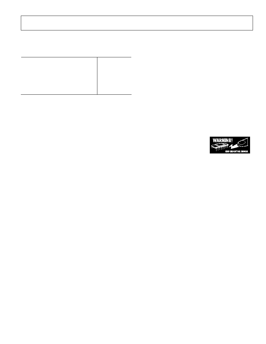
00533-C-002
+223°
50°
+273°
0°
+298°
+25°
+323°
+50°
+373°
+100°
+423°
+150°
100°
0°
+100°
+200°
+300°
+32°
+70°
+212°
°K
°C
°F
(
)
(
)
7
.
459
32
5
9
15
.
273
32
9
5
+
=
+
=
+
=
-
=
F
R
C
F
C
K
F
C
o
o
o
o
o
o
o
Figure 2. Temperature Scale Conversion Equations
AD590
Rev. C | Page 5 of 16
ABSOLUTE MAXIMUM RATINGS
Table 3.
Parameter Rating
Forward Voltage ( E+ or E)
44 V
Reverse Voltage (E+ to E)
-20 V
Breakdown Voltage (Case E+ or E)
±200 V
Rated Performance Temperature Range
1
-55°C to +150°C
Storage Temperature Range
1
-65°C to +155°C
Lead Temperature (Soldering, 10 sec)
300°C
1
The AD590 has been used at 100°C and +200°C for short periods of
measurement with no physical damage to the device. However, the absolute
errors specified apply to only the rated performance temperature range.
Stresses above those listed under Absolute Maximum Ratings
may cause permanent damage to the device. This is a stress
rating only and functional operation of the device at these or
any other conditions above those indicated in the operational
section of this specification is not implied. Exposure to absolute
maximum rating conditions for extended periods may affect
device reliability.
ESD CAUTION
ESD (electrostatic discharge) sensitive device. Electrostatic charges as high as 4000 V readily accumulate on
the human body and test equipment and can discharge without detection. Although this product features
proprietary ESD protection circuitry, permanent damage may occur on devices subjected to high energy
electrostatic discharges. Therefore, proper ESD precautions are recommended to avoid performance
degradation or loss of functionality.
Document Outline