 | ÐлекÑÑоннÑй компоненÑ: AD592BN | СкаÑаÑÑ:  PDF PDF  ZIP ZIP |
Äîêóìåíòàöèÿ è îïèñàíèÿ www.docs.chipfind.ru
CONNECTION DIAGRAM
PIN 3
PIN 2
PIN 1
()
(NC)
(+)
PIN 2 CAN BE EITHER ATTACHED OR UNCONNECTED
BOTTOM VIEW
*
REV. A
Information furnished by Analog Devices is believed to be accurate and
reliable. However, no responsibility is assumed by Analog Devices for its
use, nor for any infringements of patents or other rights of third parties
which may result from its use. No license is granted by implication or
otherwise under any patent or patent rights of Analog Devices.
a
AD592*
One Technology Way, P.O. Box 9106, Norwood, MA 02062-9106, U.S.A.
Tel: 617/329-4700
Fax: 617/326-8703
Low Cost, Precision IC
Temperature Transducer
FEATURES
High Precalibrated Accuracy: 0.5 C max @ +25 C
Excellent Linearity: 0.15 C max (0 C to +70 C)
Wide Operating Temperature Range: 25 C to +105 C
Single Supply Operation: +4 V to +30 V
Excellent Repeatability and Stability
High Level Output: 1
A/K
Two Terminal Monolithic IC: Temperature In/
Current Out
Minimal Self-Heating Errors
PRODUCT DESCRIPTION
The AD592 is a two terminal monolithic integrated circuit tem-
perature transducer that provides an output current propor-
tional to absolute temperature. For a wide range of supply
voltages the transducer acts as a high impedance temperature
dependent current source of 1
µ
A/K. Improved design and laser
wafer trimming of the IC's thin film resistors allows the AD592
to achieve absolute accuracy levels and nonlinearity errors previ-
ously unattainable at a comparable price.
The AD592 can be employed in applications between 25
°
C
and +105
°
C where conventional temperature sensors (i.e., ther-
mistor, RTD, thermocouple, diode) are currently being used.
The inherent low cost of a monolithic integrated circuit in a
plastic package, combined with a low total parts count in any
given application, make the AD592 the most cost effective tem-
perature transducer currently available. Expensive linearization
circuitry, precision voltage references, bridge components, resis-
tance measuring circuitry and cold junction compensation are
not required with the AD592.
Typical application areas include: appliance temperature sens-
ing, automotive temperature measurement and control, HVAC
(heating/ventilating/air conditioning) system monitoring, indus-
trial temperature control, thermocouple cold junction compen-
sation, board-level electronics temperature diagnostics,
temperature readout options in instrumentation, and tempera-
ture correction circuitry for precision electronics. Particularly
useful in remote sensing applications, the AD592 is immune to
voltage drops and voltage noise over long lines due to its high
impedance current output. AD592s can easily be multiplexed;
the signal current can be switched by a CMOS multiplexer or
the supply voltage can be enabled with a tri-state logic gate.
The AD592 is available in three performance grades: the
AD592AN, AD592BN and AD592CN. All devices are pack-
aged in a plastic TO-92 case rated from 45
°
C to +125
°
C. Per-
formance is specified from 25
°
C to +105
°
C. AD592 chips are
also available, contact the factory for details.
*Protected by Patent No. 4,123,698.
PRODUCT HIGHLIGHTS
1. With a single supply (4 V to 30 V) the AD592 offers
0.5
°
C temperature measurement accuracy.
2. A wide operating temperature range (25
°
C to +105
°
C)
and highly linear output make the AD592 an ideal sub-
stitute for older, more limited sensor technologies (i.e.,
thermistors, RTDs, diodes, thermocouples).
3. The AD592 is electrically rugged; supply irregularities
and variations or reverse voltages up to 20 V will not
damage the device.
4. Because the AD592 is a temperature dependent current
source, it is immune to voltage noise pickup and IR
drops in the signal leads when used remotely.
5. The high output impedance of the AD592 provides
greater than 0.5
°
C/V rejection of supply voltage drift and
ripple.
6. Laser wafer trimming and temperature testing insures
that AD592 units are easily interchangeable.
7. Initial system accuracy will not degrade significantly over
time. The AD592 has proven long term performance
and repeatability advantages inherent in integrated cir-
cuit design and construction.
378
343
273
248
1µA/
o
K
45
25
0
+70
+105 +125
TEMPERATURE
o
C
I
OUT
µA
ORDERING GUIDE
Max Cal
Max Error
Max Nonlinearity
Package
Model
Error @ +25 C
25 C to +105 C
25 C to +105 C
Option
AD592CN
0.5
°
C
1.0
°
C
0.35
°
C
TO-92
AD592BN
1.0
°
C
2.0
°
C
0.4
°
C
TO-92
AD592AN
2.5
°
C
3.5
°
C
0.5
°
C
TO-92
AD592SPECIFICATIONS
AD592AN
AD592BN
AD592CN
Model
Min
Typ
Max
Min
Typ
Max
Min Typ
Max
Units
ACCURACY
Calibration Error @ +25
°
C
1
1.5
2.5
0.7
1.0
0.3
0.5
°
C
T
A
= 0
°
C to +70
°
C
Error over Temperature
1.8
3.0
0.8
1.5
0.4
0.8
°
C
Nonlinearity
2
0.15
0.35
0.1
0.25
0.05
0.15
°
C
T
A
= 25
°
C to +105
°
C
Error over Temperature
3
2.0
3.5
0.9
2.0
0.5
1.0
°
C
Nonlinearity
2
0.25
0.5
0.2
0.4
0.1
0.35
°
C
OUTPUT CHARACTERISTICS
Nominal Current Output
@ +25
°
C (298.2K)
298.2
298.2
298.2
µ
A
Temperature Coefficient
1
1
1
µ
A/
°
C
Repeatability
4
0.1
0.1
0.1
°
C
Long Term Stability
5
0.1
0.1
0.1
°
C/month
ABSOLUTE MAXIMUM RATINGS
Operating Temperature
25
+105
25
+105
25
+105
°
C
Package Temperature
6
45
+125
45
+125
45
+125
°
C
Forward Voltage (+ to )
44
44
44
V
Reverse Voltage ( to +)
20
20
20
V
Lead Temperature
(Soldering 10 sec)
300
300
300
°
C
POWER SUPPLY
Operating Voltage Range
4
30
4
30
4
30
V
Power Supply Rejection
+4 V < V
S
< +5 V
0.5
0.5
0.5
°
C/V
+5 V < V
S
< +15 V
0.2
0.2
0.2
°
C/V
+15 V < V
S
< +30 V
0.1
0.1
0.1
°
C/V
NOTES
1
An external calibration trim can be used to zero the error @ +25
°
C.
2
Defined as the maximum deviation from a mathematically best fit line.
3
Parameter tested on all production units at +105
°
C only. C grade at 25
°
C also.
4
Maximum deviation between +25
°
C readings after a temperature cycle between 45
°
C and +125
°
C. Errors of this type are noncumulative.
5
Operation @ +125
°
C, error over time is noncumulative.
6
Although performance is not specified beyond the operating temperature range, temperature excursions within the package temperature range will not damage the device.
Specifications subject to change without notice.
Specifications shown in boldface are tested on all production units at final electrical test. Results from those tests are used to calculate outgoing quality levels. All min
and max specifications are guaranteed, although only those shown in boldface are tested on all production units.
(typical @ T
A
= +25 C, V
S
= +5 V, unless otherwise noted)
TEMPERATURE SCALE CONVERSION EQUATIONS
METALIZATION DIAGRAM
66MILS
42MILS
V+
V
REV. A
2
°
R =
°
F +459.7
K =
°
C +273.15
C =
5
9
( F 32)
F =
9
5
C +32
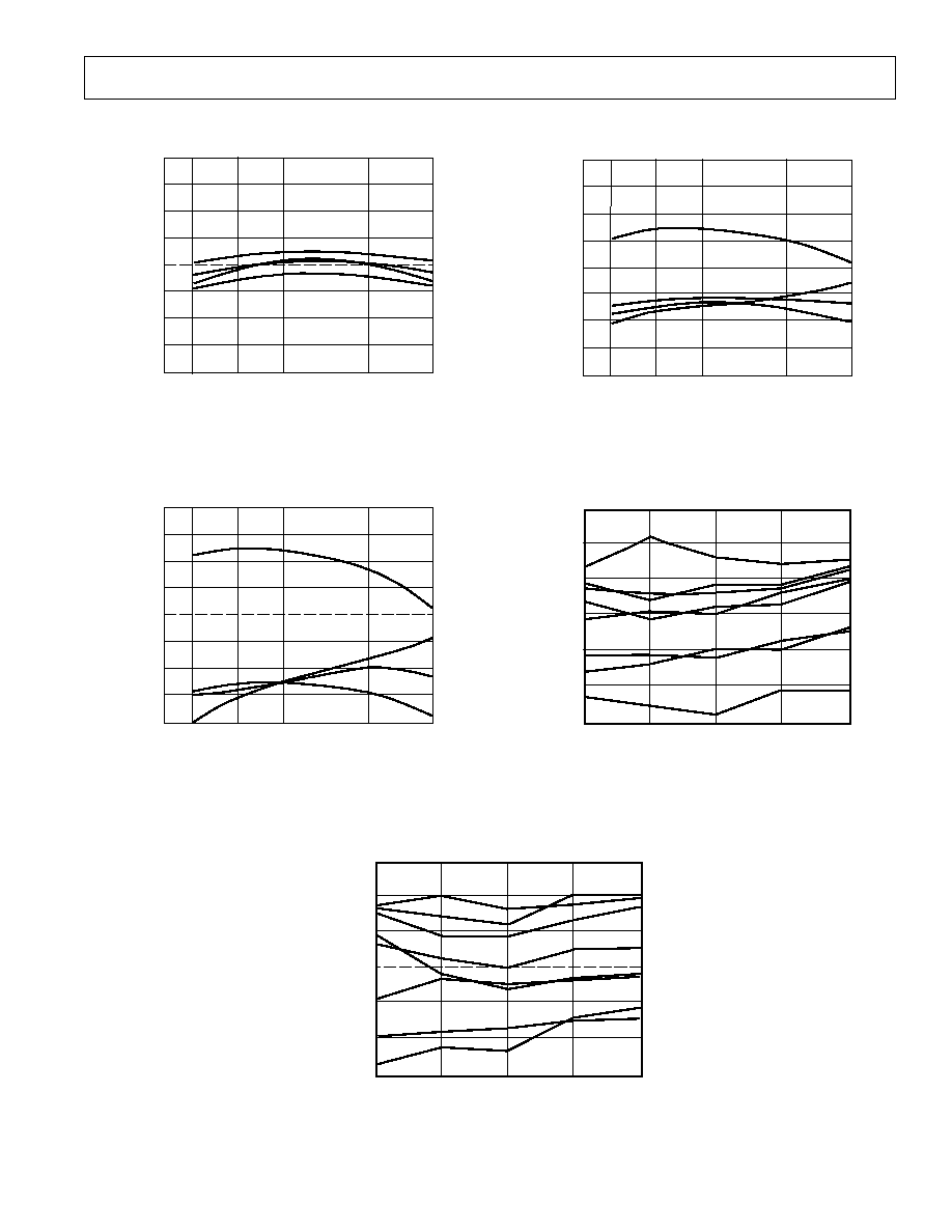
Typical Performance CurvesAD592
Typical @ V
S
= +5 V
TOTAL ERROR
o
C
TEMPERATURE
o
C
25
0
+25
+70
+105
+2.0
+1.5
+1.0
+0.5
0
0.5
1.0
1.5
2.0
AD592CN Accuracy Over Temperature
+2.0
+1.5
+1.0
+0.5
0
0.5
1.0
1.5
2.0
25
0
+25
+70
+105
TEMPERATURE
o
C
TOTAL ERROR
o
C
AD592AN Accuracy Over Temperature
TOTAL ERROR
o
C
TEMPERATURE
o
C
25
0
+25
+70
+105
+2.0
+1.5
+1.0
+0.5
0
0.5
1.0
1.5
2.0
AD592BN Accuracy Over Temperature
0.75
0.50
0.25
0
0.25
0.50
0.75
0
500
1000
1500
2000
TIME Hours
TOTAL ERROR
o
C
Long-Term Stability @ +85
°
C and 85% Relative Humidity
REV. A
3
0.75
0.50
0.25
0
0.25
0.50
0.75
0
500
1000
1500
2000
TIME Hours
TOTAL ERROR
o
C
Long-Term Stability @ +125
°
C
AD592
REV. A
4
THEORY OF OPERATION
The AD592 uses a fundamental property of silicon transistors
to realize its temperature proportional output. If two identical
transistors are operated at a constant ratio of collector current
densities, r, then the difference in base-emitter voltages will be
(kT/q)(ln r). Since both k, Boltzman's constant and q, the
charge of an electron are constant, the resulting voltage is
directly Proportional To Absolute Temperature (PTAT). In the
AD592 this difference voltage is converted to a PTAT current
by low temperature coefficient thin film resistors. This PTAT
current is then used to force the total output current to be pro-
portional to degrees Kelvin. The result is a current source with
an output equal to a scale factor times the temperature (K) of
the sensor. A typical V-I plot of the circuit at +25
°
C and the
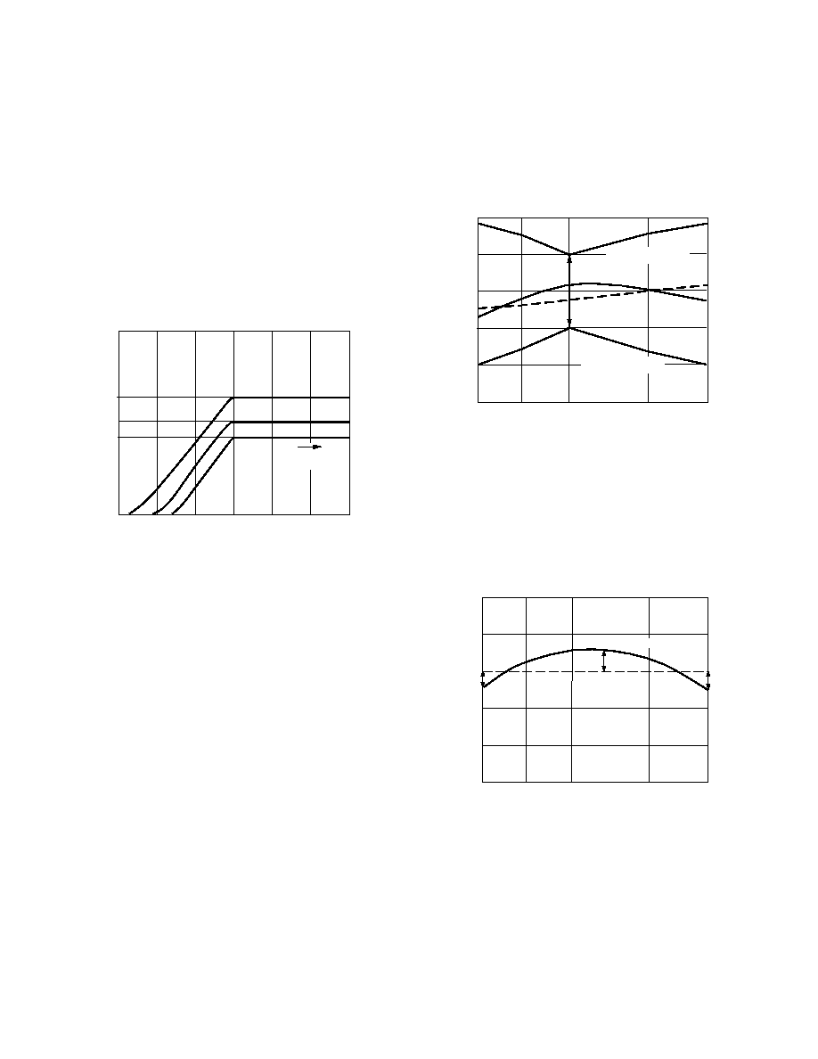
temperature extremes is shown in Figure 1.
SUPPLY VOLTAGE Volts
378
248
0
6
1
I
OUT
µA
2
3
4
5
298
+105
o
C
+25
o
C
25
o
C
UP TO
30V
Figure 1. V-I Characteristics
Factory trimming of the scale factor to 1
µ
A/K is accomplished
at the wafer level by adjusting the AD592's temperature reading
so it corresponds to the actual temperature. During laser trim-
ming the IC is at a temperature within a few degrees of 25
°
C
and is powered by a 5 V supply. The device is then packaged
and automatically temperature tested to specification.
FACTORS AFFECTING AD592 SYSTEM PRECISION
The accuracy limits given on the Specifications page for the
AD592 make it easy to apply in a variety of diverse applications.
To calculate a total error budget in a given system it is impor-
tant to correctly interpret the accuracy specifications, non-
linearity errors, the response of the circuit to supply voltage
variations and the effect of the surrounding thermal environ-
ment. As with other electronic designs external component se-
lection will have a major effect on accuracy.
CALIBRATION ERROR, ABSOLUTE ACCURACY AND
NONLINEARITY SPECIFICATIONS
Three primary limits of error are given for the AD592 such that
the correct grade for any given application can easily be chosen
for the overall level of accuracy required. They are the calibra-
tion accuracy at +25
°
C, and the error over temperature from
0
°
C to +70
°
C and 25
°
C to +105
°
C. These specifications cor-
respond to the actual error the user would see if the current out-
put of an AD592 were converted to a voltage with a precision
resistor. Note that the maximum error at room temperature,
over the commercial IC temperature range, or an extended
range including the boiling point of water, can be directly read
from the specifications table. All three error limits are a combi-
nation of initial error, scale factor variation and nonlinearity de-
viation from the ideal 1
µ
A/K output. Figure 2 graphically
depicts the guaranteed limits of accuracy for an AD592CN.
TEMPERATURE
o
C
+1.0
+0.5
25
+105
0
+25
+70
0
0.5
1.0
TOTAL ERROR
o
C
MAXIMUM ERROR
OVER TEMPERATURE
TYPICAL ERROR
CALIBRATION
ERROR LIMIT
MAXIMUM ERROR
OVER TEMPERATURE
Figure 2. Error Specifications (AD592CN)
The AD592 has a highly linear output in comparison to older
technology sensors (i.e., thermistors, RTDs and thermo-
couples), thus a nonlinearity error specification is separated
from the absolute accuracy given over temperature. As a maxi-
mum deviation from a best-fit straight line this specification rep-
resents the only error which cannot be trimmed out. Figure 3 is
a plot of typical AD592CN nonlinearity over the full rated tem-
perature range.
TYPICAL NONLINEARITY
+0.2
+0.1
25
+105
0
+25
+70
0
0.1
0.2
TEMPERATURE
o
C
NONLINEARITY
o
C
Figure 3. Nonlinearity Error (AD592CN)
TRIMMING FOR HIGHER ACCURACY
Calibration error at 25
°
C can be removed with a single tempera-
ture trim. Figure 4 shows how to adjust the AD592's scale fac-
tor in the basic voltage output circuit.
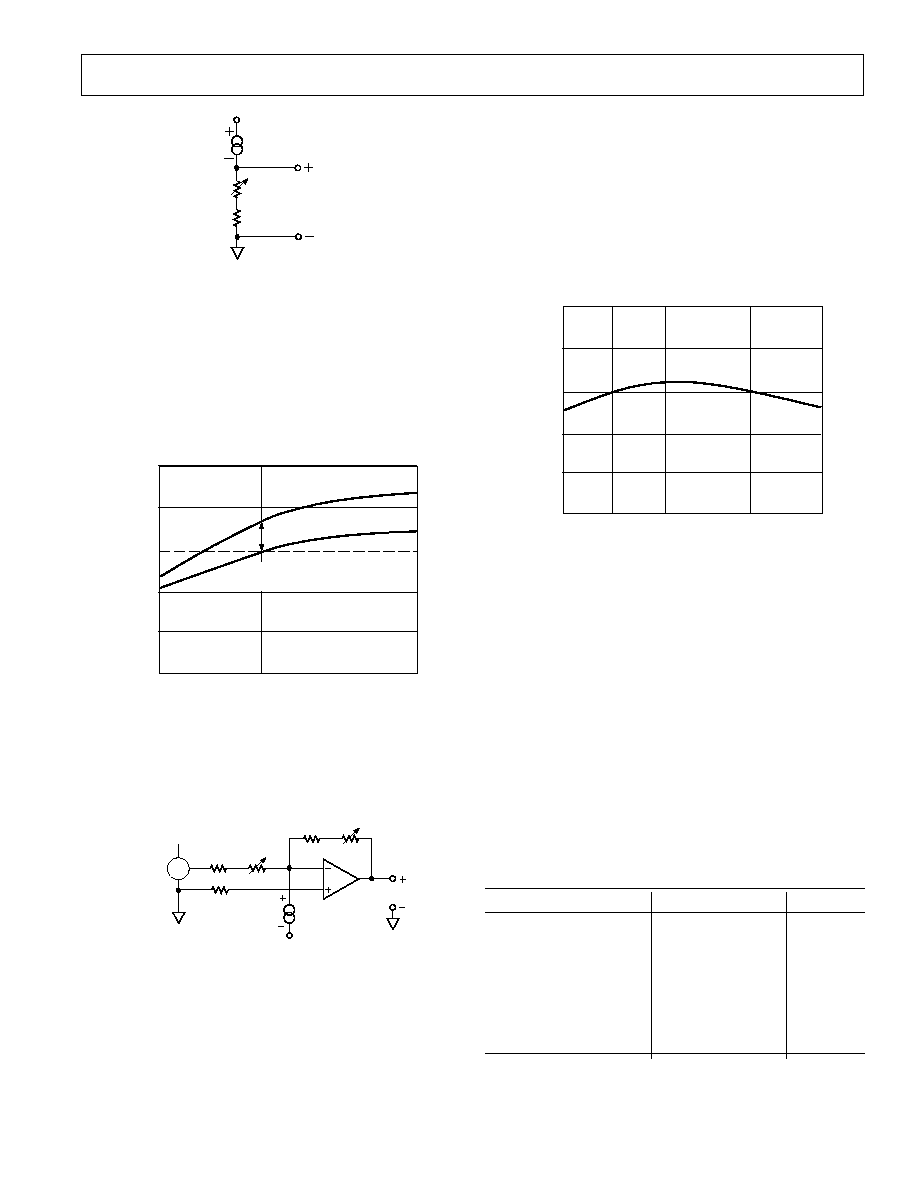
AD592
REV. A
5
+V
AD592
R
100
950
V
OUT
= 1mV/K
Figure 4. Basic Voltage Output (Single Temperature Trim)
To trim the circuit the temperature must be measured by a ref-
erence sensor and the value of R should be adjusted so the out-
put (V
OUT
) corresponds to 1 mV/K. Note that the trim
procedure should be implemented as close as possible to the
temperature highest accuracy is desired for. In most applications
if a single temperature trim is desired it can be implemented
where the AD592 current-to-output voltage conversion takes
place (e.g., output resistor, offset to an op amp). Figure 5 illus-
trates the effect on total error when using this technique.
AFTER SINGLE
TEMPERATURE
CALIBRATION
ACCURACY
WITHOUT TRIM
+1.0
+0.5
25
+105
+25
0
0.5
1.0
TEMPERATURE
o
C
TOTAL ERROR
o
C
Figure 5. Effect of Scale Factor Trim on Accuracy
If greater accuracy is desired, initial calibration and scale factor
errors can be removed by using the AD592 in the circuit of
Figure 6.
8.66k
R1
1k
97.6k
R2
5k
7.87k
AD741
V
OUT
= 100mV/
o
C
+5V
AD1403
V
AD592
Figure 6. Two Temperature Trim Circuit
With the transducer at 0
°
C adjustment of R1 for a 0 V output
nulls the initial calibration error and shifts the output from K to
°
C. Tweaking the gain of the circuit at an elevated temperature
by adjusting R2 trims out scale factor error. The only error
remaining over the temperature range being trimmed for is
nonlinearity. A typical plot of two trim accuracy is given in
Figure 7.
SUPPLY VOLTAGE AND THERMAL ENVIRONMENT
EFFECTS
The power supply rejection characteristics of the AD592 mini-
mizes errors due to voltage irregularity, ripple and noise. If a
supply is used other than 5 V (used in factory trimming), the
power supply error can be removed with a single temperature
trim. The PTAT nature of the AD592 will remain unchanged.
The general insensitivity of the output allows the use of lower
cost unregulated supplies and means that a series resistance of
several hundred ohms (e.g., CMOS multiplexer, meter coil
resistance) will not degrade the overall performance.
+2.0
+1.0
25
+105
+25
0
1.0
2.0
TEMPERATURE
o
C
TOTAL ERROR
o
C
0
+75
Figure 7. Typical Two Trim Accuracy
The thermal environment in which the AD592 is used deter-
mines two performance traits: the effect of self-heating on accu-
racy and the response time of the sensor to rapid changes in
temperature. In the first case, a rise in the IC junction tempera-
ture above the ambient temperature is a function of two vari-
ables; the power consumption level of the circuit and the
thermal resistance between the chip and the ambient environ-
ment (
JA
). Self-heating error in
°
C can be derived by multiply-
ing the power dissipation by
JA
. Because errors of this type can
vary widely for surroundings with different heat sinking capaci-
ties it is necessary to specify
JA
under several conditions. Table
I shows how the magnitude of self-heating error varies relative
to the environment. In typical free air applications at +25
°
C
with a 5 V supply the magnitude of the error is 0.2
°
C or less. A
common clip-on heat sink will reduce the error by 25% or more
in critical high temperature, large supply voltage situations.
Table I. Thermal Characteristics
Medium
JA
(
°
C/watt)
(sec)*
Still Air
Without Heat Sink
175
60
With Heat Sink
130
55
Moving Air
Without Heat Sink
60
12
With Heat Sink
40
10
Fluorinert Liquid
35
5
Aluminum Block**
30
2.4
NOTES
*
is an average of five time constants (99.3% of final value). In cases where the
thermal response is not a simple exponential function, the actual thermal re-
sponse may be better than indicated.
**With thermal grease.