 | ÐлекÑÑоннÑй компоненÑ: AD606J | СкаÑаÑÑ:  PDF PDF  ZIP ZIP |
AD606 50MHz, 80dB Demodulating Logarithmic Amplifier with Limiter Output
REV. 0
Information furnished by Analog Devices is believed to be accurate and
reliable. However, no responsibility is assumed by Analog Devices for its
use, nor for any infringements of patents or other rights of third parties
which may result from its use. No license is granted by implication or
otherwise under any patent or patent rights of Analog Devices.
a
50 MHz, 80 dB Demodulating
Logarithmic Amplifier with Limiter Output
AD606
One Technology Way, P.O. Box 9106, Norwood, MA 02062-9106, U.S.A.
Tel: 617/329-4700
Fax: 617/326-8703
FEATURES
Logarithmic Amplifier Performance
75 dBm to +5 dBm Dynamic Range
1.5 nV/
Hz Input Noise
Usable to >50 MHz
37.5 mV/dB Voltage Output
On-Chip Low-Pass Output Filter
Limiter Performance
1 dB Output Flatness over 80 dB Range
3 Phase Stability at 10.7 MHz over 80 dB Range
Adjustable Output Amplitude
Low Power
+5 V Single Supply Operation
65 mW Typical Power Consumption
CMOS Compatible Power-Down to 325 W typ
<5 s Enable/Disable Time
APPLICATIONS
Ultrasound and Sonar Processing
Phase-Stable Limiting Amplifier to 100 MHz
Received Signal Strength Indicator (RSSI)
Wide Range Signal and Power Measurement
PRODUCT DESCRIPTION
The AD606 is a complete, monolithic logarithmic amplifier
using a 9-stage "successive-detection" technique. It provides
both logarithmic and limited outputs. The logarithmic output is
from a three-pole post-demodulation low-pass filter and provides
a loadable output voltage of +0.1 V dc to +4 V dc. The logarith-
mic scaling is such that the output is +0.5 V for a sinusoidal in-
put of 75 dBm and +3.5 V at an input of +5 dBm; over this
range the logarithmic linearity is typically within
±
0.4 dB. All
scaling parameters are proportional to the supply voltage.
The AD606 can operate above and below these limits, with re-
duced linearity, to provide as much as 90 dB of conversion
range. A second low-pass filter automatically nulls the input off-
set of the first stage down to the submicrovolt level. Adding ex-
ternal capacitors to both filters allows operation at input
frequencies as low as a few hertz.
The AD606's limiter output provides a hard-limited signal out-
put as a differential current of
±
1.2 mA from open-collector
outputs. In a typical application, both of these outputs are
loaded by 200
resistors to provide a voltage gain of more than
90 dB from the input. Transition times are 1.5 ns, and the
phase is stable to within
±
3
°
at 10.7 MHz for signals from
75 dBm to +5 dBm.
The logarithmic amplifier operates from a single +5 V supply
and typically consumes 65 mW. It is enabled by a CMOS logic
level voltage input, with a response time of <5
µ
s. When dis-
abled, the standby power is reduced to <1 mW within 5
µ
s.
The AD606J is specified for the commercial temperature range
of 0
°
C to +70
°
C and is available in 16-pin plastic DIPs or
SOICs. Consult the factory for other packages and temperature
ranges.
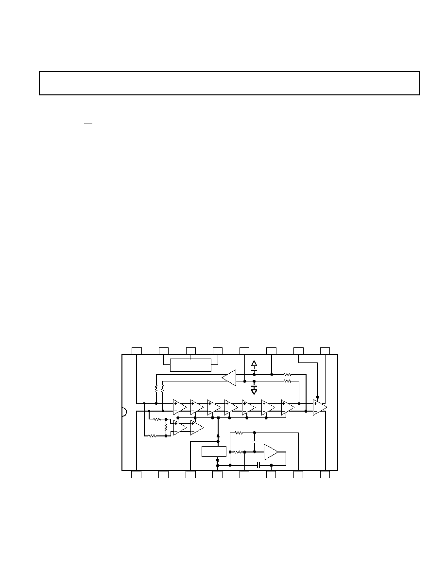
FUNCTIONAL BLOCK DIAGRAM
LMLO
OPCM
VLOG
BFIN
ILOG
COMM
INLO
ISUM
3
2
1
4
5
6
8
7
14
15
16
13
12
11
9
10
LADJ
FIL1
FIL2
VPOS
PRUP
COMM
LMHI
INHI
X2
RE FERE NCE
AND PO WE R UP
OFFSET-NULL
LOW-PASS FILTER
AD606
HIGH-END
DETECTORS
FINAL
LIMITER
9.375k
9.375k
12
µ
A/dB
MAIN SIGNAL PATH
11.15 dB/STAGE
2
µ
A/dB
1.5k
30k
250
30k
X1
360k
1.5k
30pF
30pF
TWO-POLE
SALLEN-KEY
FILTER
2pF
360k
ONE-POLE
FILTER
2pF

AD606SPECIFICATIONS
(@ T
A
= +25 C and supply = +5 V unless otherwise noted; dBm assumes 50
)
REV. 0
2
Model
AD606J
Parameter
Conditions
Min
Typ
Max
Units
SIGNAL INPUT
Log Amp f
MAX
AC Coupled; Sinusoidal Input
50
MHz
Limiter f
MAX
AC Coupled; Sinusoidal Input
100
MHz
Dynamic Range
80
dB
Input Resistance
Differential Input
500
2,500
Input Capacitance
Differential Input
2
pF
SIGNAL OUTPUT
Limiter Flatness
75 dBm to +5 dBm Input Signal at 10.7 MHz
1.5
+1.5
dB
With Pin 9 to V
POS
via a 200
Resistor
and Pin 8 to V
POS
via a 200
Resistor
Output Current
At Pins 8 or 9, Proportional to V
POS
, LADJ Grounded
1.2
mA
LADJ Open Circuited
0.48
mA
Phase Variation with Input Level
75 dBm to +5 dBm Input Signal at 10.7 MHz
±
3
°
LOG (RSSI ) OUTPUT
Nominal Slope
At 10.7 MHz; (0.0075
×
V
POS
)/dB
37.5
mV/dB
At 45 MHz
35
mV/dB
Slope Accuracy
Untrimmed at 10.7 MHz
15
±
5
+15
%
Intercept
Sinusoidal Input; Independent of V
POS
88.33
dBm
Logarithmic Conformance
75 dBm to +5 dBm Input Signal at 10.7 MHz
1.5
0.4
+1.5
dB
Nominal Output
Input Level = 75 dBm
0.5
V
Input Level = 35 dBm
2
V
Input Level = +5 dBm
3.5
V
Accuracy over Temperature
After Calibration at 35 dBm at 10.7 MHz
3
3
dB
T
MIN
to T
MAX
Video Response Time
From Onset of Input Signal Until Output Reaches
400
ns
95% of Final Value
POWER-DOWN INTERFACE
Power-Up Response Time
Time Delay Following HI Transition Until
3.5
µ
s
Device Meets Full Specifications
AC Coupled with 100 pF Coupling Capacitors
Input Bias Current
Logical HI Input (See Figure 12)
1
nA
Logical LO Input
4
µ
A
POWER SUPPLY
Operating Range
4.5
5.5
V
Powered-Up Current
Zero Signal Input
13
mA
T
MIN
to T
MAX
13
20
mA
Powered-Down Current
T
MIN
to T
MAX
65
200
µ
A
Specifications shown in boldface are tested on all production units at final electrical test. Results from those tests are used to calculate outgoing quality levels. All min
and max specifications are guaranteed, although only those shown in boldface are tested on all production units.
Specifications subject to change without notice.
AD606
REV. 0
3
ORDERING GUIDE
Temperature
Model
Range
Package Option
AD606JN 0
°
C to +70
°
C 16-Pin Plastic DIP (N-16)
AD606JR 0
°
C to +70
°
C 16-Pin Narrow-Body SOIC (R-16A)
PIN DESCRIPTION
Plastic DIP (N)
and
Small Outline (R)
Packages
INLO
COMM
ILOG
BFIN
ISUM
VLOG
OPCM
LMLO
LMHI
LADJ
FIL2
FIL1
VPOS
PRUP
COMM
INHI
1
2
3
4
5
6
7
8
16
15
14
13
12
11
10
9
TOP VIEW
(Not to Scale)
AD606
ABSOLUTE MAXIMUM RATINGS
1
Supply Voltage V
POS
. . . . . . . . . . . . . . . . . . . . . . . . . . . . +9 V
Internal Power Dissipation
2
. . . . . . . . . . . . . . . . . . . 600 mW
Operating Temperature Range . . . . . . . . . . . . . 0
°
C to +70
°
C
Storage Temperature Range . . . . . . . . . . . . 65
°
C to +150
°
C
Lead Temperature Range (Soldering 60 sec) . . . . . . . . +300
°
C
NOTES
1
Stresses above those listed under "Absolute Maximum Ratings" may cause
permanent damage to the device. This is a stress rating only and functional
operation of the device at these or any other conditions above those indicated in the
operational section of this specification is not implied. Exposure to absolute
maximum rating conditions for extended periods may affect device reliability.
2
Specification is for device in free air:
16-Pin Plastic DIP Package:
JA
= 85
°
C/Watt
16-Pin SOIC Package:
JA
= 100
°
C/Watt
WARNING!
ESD SENSITIVE DEVICE
CAUTION
ESD (electrostatic discharge) sensitive device. Electrostatic charges as high as 4000 V readily
accumulate on the human body and test equipment and can discharge without detection.
Although the AD606 features proprietary ESD protection circuitry, permanent damage may
occur on devices subjected to high energy electrostatic discharges. Therefore, proper ESD
precautions are recommended to avoid performance degradation or loss of functionality.
PIN FUNCTIONS
Pin Mnemonic Function
1
INLO
DIFFERENTIAL RF INPUT
75 dBm to +5 dBm, Inverting, AC Coupled.
2
COMM
POWER SUPPLY COMMON
Connect to Ground.
3
ISUM
LOG DETECTOR SUMMING NODE
4
ILOG
LOG CURRENT OUTPUT
Normally No Connection; 2
µ
A/dB Output
Current.
5
BFIN
BUFFER INPUT
Optionally Used to Realize Low Frequency
Post-Demodulation Filters.
6
VLOG
BUFFERED LOG OUTPUT
37.5 mV/dB (100 mV to 4.5 V).
7
OPCM
OUTPUT COMMON
Connect to Ground.
8
LMLO
DIFFERENTIAL LIMITER OUTPUT
1.2 mA Full-Scale Output Current. Open
Collector Output Must Be "Pulled" Up to
VPOS with R
400
.
9
LMHI
DIFFERENTIAL LIMITER OUTPUT
1.2 mA Full-Scale Output Current. Open
Collector Output Must Be "Pulled" Up to
VPOS with R
400
.
10
LADJ
LIMITER LEVEL ADJUSTMENT
Optionally Used to Adjust Limiter Output
Current.
11
FIL1
OFFSET LOOP LOW-PASS FILTER
Normally No Connection; a Capacitor Between
FIL1 and FIL2 May Be Added to Lower the
Filter Cutoff Frequency.
12
FIL2
OFFSET LOOP LOW-PASS FILTER
Normally No Connection; See Above.
13
VPOS
POSITIVE SUPPLY
Connect to +5 V at 13 mA.
14
PRUP
POWER UP
CMOS (5 V) Logical High = Device On
(
65 mW).
CMOS (0 V) Logical Low = Device Off
(
325
µ
W).
15
COMM
POWER SUPPLY COMMON
Connect to Ground.
16
INHI
DIFFERENTIAL RF INPUT
75 dBm to +5 dBm, Noninverting, AC Coupled.
AD606
REV. 0
4
INPUT LEVEL CONVENTIONS
RF logarithmic amplifiers usually have their input specified in
"dBm," meaning "decibels with respect to 1 mW." Unfortu-
nately, this is not precise for several reasons.
1. Log amps respond not to power but to voltage. In this re-
spect, it would be less ambiguous to use "dBV" (decibels
referred to 1 V) as the input metric. Also, power is dependent
on the rms (root mean-square) value of the signal, while log
amps are not inherently rms responding.
2. The response of a demodulating log amp depends on the
waveform. Convention assumes that the input is sinusoidal.
However, the AD606 is capable of accurately handling any
input waveform, including ac voltages, pulses and square
waves, Gaussian noise, and so on. See the AD640 data sheet,
which covers the effect of waveform on logarithmic intercept,
for more information.
3. The impedance in which the specified power is measured is
not always stated. In the log amp context it is invariably as-
sumed to be 50
. Thus, 0 dBm means "1 mW rms in 50
,"
and corresponds to an rms voltage of
(1 mW
×
50
),
or
224 mV.
Popular convention requires the use of dBm to simplify the
comparison of log amp specifications. Unless otherwise stated,
sinusoidal inputs expressed as dBm in 50
are used to specify
the performance of the AD606 throughout this data sheet. We
will also show the corresponding rms voltages where it helps to
clarify the specification. Noise levels will likewise be given in
dBm; the response to Gaussian noise is 0.5 dB higher than for a
sinusoidal input of the same rms value.
Note that dynamic range, being a simple ratio, is always speci-
fied simply as "dB", and the slope of the logarithmic transfer
function is correctly specified as "mV/dB," NOT as "mV/dBm."
LOGARITHMIC SLOPE AND INTERCEPT
A generalized logarithmic amplifier having an input voltage V
IN
and output voltage V
LOG
must satisfy a transfer function of the
form
V
LOG
=
V
Y
log
10
( V
IN
/ V
X
)
where, in the case of the AD606, the voltage V
IN
is the differ-
ence between the voltages on pins INHI and INLO, and the
voltage V
LOG
is that measured at the output pin VLOG. V
Y
and
V
X
are fixed voltages that determine the slope and intercept of
the logarithmic amplifier, respectively. These parameters are
inherent in the design of a particular logarithmic amplifier,
although may be adjustable, as in the AD606. When V
IN
= V
X
,
the logarithmic argument is one, hence the logarithm is zero. V
X
is, therefore, called the logarithmic intercept voltage because the
output voltage V
LOG
crosses zero for this input. The slope volt-
age V
Y
is can also be interpreted as the "volts per decade" when
using base-10 logarithms as shown here.
Note carefully that V
LOG
and VLOG in the above paragraph
(and elsewhere in this data sheet) are different. The first is a
voltage; the second is a pin designation.
This equation suggests that the input V
IN
is a dc quantity, and,
if V
X
is positive, that V
IN
must likewise be positive, since the
logarithm of a negative number has no simple meaning. In fact,
in the AD606, the response is independent of the sign of V
IN
because of the particular way in which the circuit is built. This
is part of the demodulating nature of the amplifier, which
results in an alternating input voltage being transformed into a
quasi-dc (rectified and filtered) output voltage.
The single supply nature of the AD606 results in common-mode
level of the inputs INHI and INLO being at about +2.5 V (us-
ing the recommended +5 V supply). In normal ac operation,
this bias level is developed internally and the input signal is
coupled in through dc blocking capacitors. Any residual dc off-
set voltage in the first stage limits the logarithmic accuracy for
small inputs. In ac operation, this offset is automatically and
continuously nulled via a feedback path from the last stage, pro-
vided that the pins INHI and INLO are not shorted together, as
would be the case if transformer coupling were used for the signal.
While any logarithmic amplifier must eventually conform to the
basic equation shown above, which, with appropriate elabora-
tion, can also fully account for the effect of the signal waveform
on the effective intercept,
1
it is more convenient in RF applica-
tions to use a simpler expression. This simplification results
from first, assuming that the input is always sinusoidal, and sec-
ond, using a decibel representation for the input level. The stan-
dard representation of RF levels is (incorrectly, in a log amp
context) in terms of power, specifically, decibels above 1 milli-
watt (dBm) with a presumed impedance level of 50
. That be-
ing the case, we can rewrite the transfer function as
V
LOG
=
V
Y
(P
IN
P
X
)
where it must be understood that P
IN
means the sinusoidal input
power level in a 50
system, expressed in dBm, and P
X
is the
intercept, also expressed in dBm. In this case, P
IN
and P
X
are
simple, dimensionless numbers. (P
X
is sometimes called the
"logarithmic offset," for reasons which are obvious from the
above equation.) V
Y
is still defined as the logarithmic slope, usu-
ally specified as so many millivolts per decibel, or mV/dB.
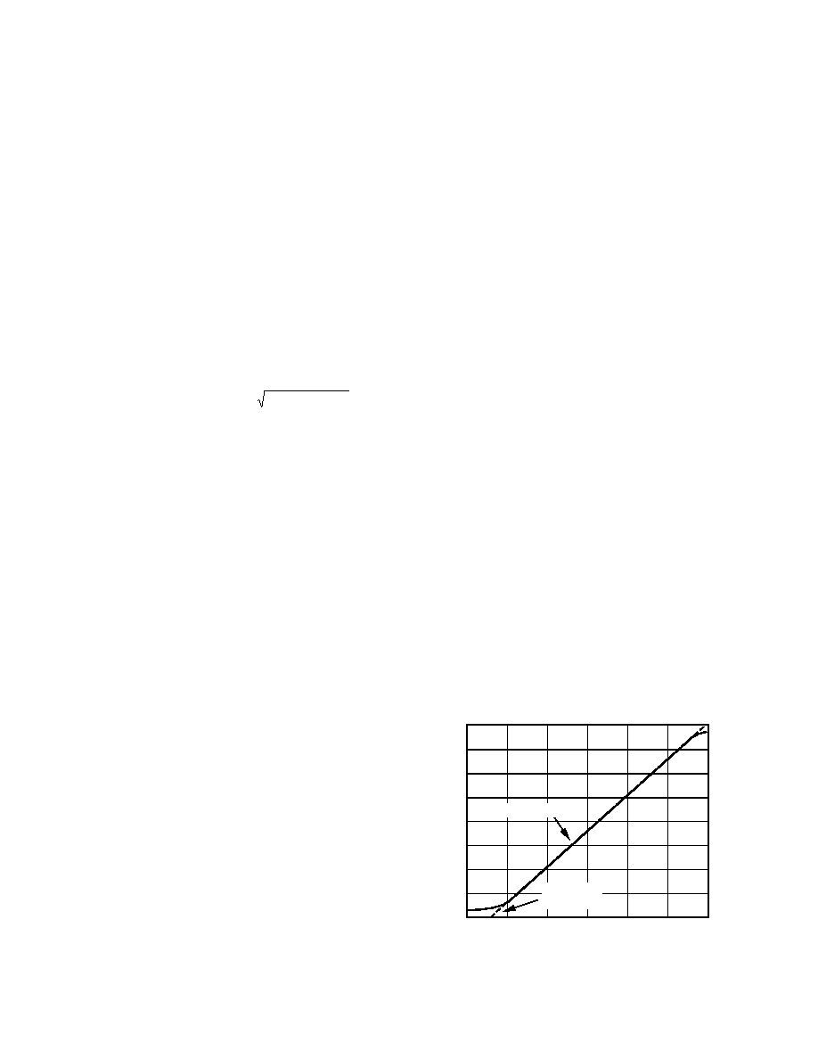
In the case of the AD606, the slope voltage, V
Y
, is nominally
750 mV when operating at V
POS
= 5 V. This can also be ex-
pressed as 37.5 mV/dB or 750 mV/decade; thus, the 80 dB
range equates to 3 V. Figure 1 shows the transfer function of the
AD606. The slope is closely proportional to V
POS
, and can more
generally be stated as V
Y
= 0.15
×
V
POS.
Thus, in those applica-
tions where the scaling must be independent of supply voltage,
this must be stabilized to the required accuracy. In applications
where the output is applied to an A/D converter, the reference
VLOG Volts DC
INPUT SIGNAL dBm
4
0
+20
1
0.5
80
100
2
1.5
2.5
3
3.5
0
20
40
60
SLOPE = 37.5mV/dB
INTERCEPT
AT 88.33dBm
Figure 1. Nominal Transfer Function
1
See, for example, the AD640 data sheet, which is published in Section 3 of
the Special Linear Reference Manual or Section 9.3 of the 1992 Amplifier
Applications Guide.
AD606
REV. 0
5
In applications where V
LOG
is taken to an A/D converter which
allows the use of an external reference, this reference input
should also be connected to the same +5 V supply. The power
supply voltage may be in the range +4.5 V to +5.5 V, providing
a range of slopes from nominally 33.75 mV/dB (675 mV/ de-
cade) to 41.25 mV/dB (825 mV/decade).
A buffer amplifier, having a gain of two, provides a final output
scaling at V
LOG
of 37.5 mV/dB (750 mV/decade). This low-
impedance output can run from close to ground to over +4 V
(using the recommended +5 V supply) and is tolerant of resis-
tive and capacitive loads. Further filtering is provided by a con-
jugate pole pair, formed by internal capacitors which are an
integral part of the output buffer. The corner frequency of the
overall filter is 2 MHz, and the 10%90% rise time is 150 ns.
Later, we will show how the slope and intercept can be altered
using simple external adjustments. The direct buffer input
BFIN is used in these cases.
The last limiter output is available as complementary currents
from open collectors at pins LMHI and LMLO. These currents
are each 1.2 mA typical with LADJ grounded and may be con-
verted to voltages using external load resistors connected to
VPOS; typically, a 200
resistor is used on just one output.
The voltage gain is then over 90 dB, resulting in a hard-limited
output for all input levels down to the noise floor. The phasing
is such that the voltage at LMHI goes high when the input
(INHI to INLO) is positive. The overall delay time from the sig-
nal inputs to the limiter outputs is 8 ns. Of particular impor-
tance is the phase stability of these outputs versus input level. At
50 MHz, the phase typically remains within
±
4
°
from 70 dBm
to +5 dBm. The rise time of this output (essentially a square
wave) is about 1.2 ns, resulting in clean operation to more than
70 MHz.
Offset-Control Loop
The offset-control loop nulls the input offset voltage, and sets
up the bias voltages at the input pins INHI and INLO. A full
understanding of this offset-control loop is useful, particularly
when using larger input coupling capacitors and an external fil-
ter capacitor to lower the minimum acceptable operating fre-
quency. The loop's primary purpose is to extend the lower end
for that converter should be a fractional part of V
POS
, if possible.
The slope is essentially independent of temperature.
The intercept P
X
is essentially independent of either the supply
voltage or temperature. However, the AD606 is not factory cali-
brated, and both the slope and intercept may need to be exter-
nally adjusted. Following calibration, the conformance to an
ideal logarithmic law will be found to be very close, particularly
at moderate frequencies (see Figure 14), and still acceptable at
the upper end of the frequency range (Figure 15).
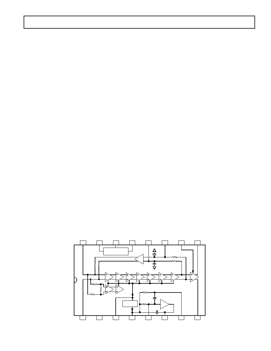
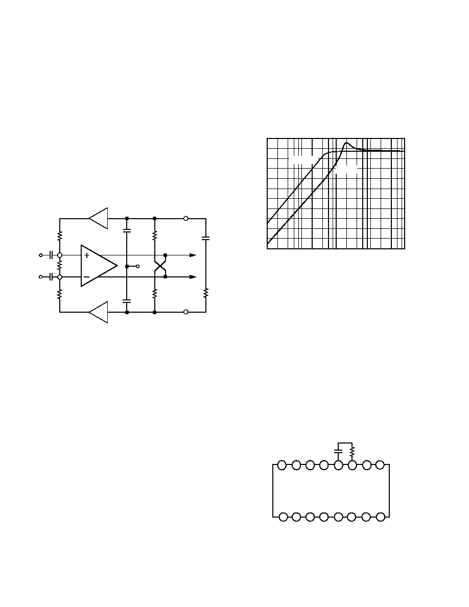
CIRCUIT DESCRIPTION
Figure 2 is a block diagram of the AD606, which is a complete
logarithmic amplifier system in monolithic form. It uses a total
of nine limiting amplifiers in a "successive detection" scheme to
closely approximate a logarithmic response over a total dynamic
range of 90 dB (Figure 2). The signal input is differential, at
nodes INHI and INLO, and will usually be sinusoidal and ac
coupled. The source may be either differential or single-sided;
the input impedance is about 2.5 k
in parallel with 2 pF. Seven
of the amplifier/detector stages handle inputs from 80 dBm
(32
µ
V rms) up to about 14 dBm (45 mV rms). The noise floor
is about 83 dBm (18
µ
V rms). Another two stages receive the
input attenuated by 22.3 dB, and respond to inputs up to
+10 dBm (707 mV rms). The gain of each of these stages is
11.15 dB and is accurately stabilized over temperature by a
precise biasing system.
The detectors provide full-wave rectification of the alternating
signal present at each limiter output. Their outputs are in the
form of currents, proportional to the supply voltage. Each cell
incorporates a low-pass filter pole, as the first step in recovering
the average value of the demodulated signal, which contains ap-
preciable energy at even harmonics of the input frequency. A
further real pole can be introduced by adding a capacitor be-
tween the summing node ISUM and VPOS. The summed de-
tector output currents are applied to a 6:1 reduction current
mirror. Its output at ILOG is scaled 2
µ
A/dB, and is converted
to voltage by an internal load resistor of 9.375 k
between
ILOG and OPCM (output common, which is usually grounded).
The nominal slope at this point is 18.75 mV/dB (375 mV/
decade).
LMLO
OPCM
VLOG
BFIN
ILOG
COMM
INLO
ISUM
3
2
1
4
5
6
8
7
14
15
16
13
12
11
9
10
LADJ
FIL1
FIL2
VPOS
PRUP
COMM
LMHI
INHI
X2
RE FERE NCE
AND PO WE R UP
OFFSET-NULL
LOW-PASS FILTER
AD606
HIGH-END
DETECTORS
FINAL
LIMITER
9.375k
9.375k
12
µ
A/dB
MAIN SIGNAL PATH
11.15 dB/STAGE
2
µ
A/dB
1.5k
30k
250
30k
X1
360k
1.5k
30pF
30pF
TWO-POLE
SALLEN-KEY
FILTER
2pF
360k
ONE-POLE
FILTER
2pF
Figure 2. AD606 Simplified Block Diagram
AD606
REV. 0
6
of the dynamic range in the case where the offset voltage of the
first stage should be high enough to cause later stages to prema-
turely enter limiting, because of the high dc gain (about 8000)
of the main amplifier system. For example, an offset voltage of
only 20
µ
V would become 160 mV at the output of the last stage
in the main amplifier (before the final limiter section), driving
the last stage well into limiting. In the absence of noise, this lim-
iting would simply result in the logarithmic output ceasing to
become any lower below a certain signal level at the input. The
offset would also degrade the logarithmic conformance in this
region. In practice, the finite noise of the first stage also plays a
role in this regard, even if the dc offset were zero.
Figure 3 shows a representation of this loop, reduced to essen-
tials. The figure closely corresponds to the internal circuitry,
and correctly shows the input resistance. Thus, the forward gain
of the main amplifier section is 7
×
11.15 dB, but the loop gain
is lowered because of the attenuation in the network formed by
+1
CF1
30pF
CF2
30pF
TO FINAL
LIMITER
STAGE
RF2
360k
RF1
360k
RB1
30k
RA
2.5k
RB2
30k
C
C2
C
C1
0V
C
Z
R
Z
FIL1
FIL2
+1
78dB
Figure 3. Offset Control Loop
RB1 and RB2 and the input resistance RA. The connection po-
larity is such as to result in negative feedback, which reduces the
input offset voltage by the dc loop gain, here about 50 dB, that
is, by a factor of about 316. We use a differential representation,
because later we will examine the consequences to the power-up
response time in the event that the ac coupling capacitors C
C1
and C
C2
do not exactly match. Note that these capacitors, as
well as forming a high-pass filter to the signal in the forward
path, also introduce a pole in the feedback path.
Internal resistors RF1 and RF2 in conjunction with grounded
capacitors CF1 and CF2 form a low-pass filter at 15 kHz. This
frequency can optionally be lowered by the addition of an exter-
nal capacitor C
Z
, and in some cases a series resistor R
Z
. This, in
conjunction with the low-pass section formed at the input cou-
pling, results in a two-pole high-pass response, falling of at
40 dB/decade below the corner frequency. The damping factor
of this filter depends on the ratio C
Z
/C
C
(when C
Z
>>C
F
) and
also on the value of R
Z
.
The inclusion of this control loop has no effect on the high frequency
response of the AD606. Nor does it have any effect on the low fre-
quency response when the input amplitude is substantially above the
input offset voltage.
The loop's effect is felt only at the lower end of the dynamic
range, that is, from about 80 dBm to 70 dBm, and when the
signal frequency is near the lower edge of the passband. Thus,
the small signal results which are obtained using the suggested
model are not indicative of the ac response at moderate to high
signal levels. Figure 4 shows the response of this model for the
default case (using C
C
= 100 pF and C
Z
= 0) and with C
Z
=
150 pF. In general, a maximally flat ac response occurs when C
Z
is roughly twice C
C
(making due allowance for the internal
30 pF capacitors). Thus, for audio applications, one can use
C
C
= 2.7
µ
F and C
Z
= 4.7
µ
F to achieve a high-pass corner
(3 dB) at 25 Hz.
90
70
20
100k
100M
10M
1M
10k
80
60
40
50
20
30
10
10
0
C
Z
= 0pF
C
Z
= 150pF
INPUT FREQUENCY Hz
RELATIVE OUTPUT dB
Figure 4. Frequency Response of Offset Control Loop for
C
Z
= 0 pF and C
Z
= 150 pF (C
C
= 100 pF)
However, the maximally flat ac response is not optimal in two
special cases. First, where the RF input level is rapidly pulsed,
the fast edges will cause the loop filter to ring. Second, ringing
can also occur when using the power-up feature, and the ac cou-
pling capacitors do not exactly match in value. We will examine
the latter case in a moment. Ringing in a linear amplifier is an-
noying, but in a log amp, with its much enhanced sensitivity to
near zero signals, it can be very disruptive.
To optimize the low level accuracy, that is, achieve a highly
damped pulse response in this filter, it is recommended to in-
clude a resistor R
Z
in series with an increased value of C
Z
. Some
experimentation may be necessary, but for operation in the
range 3 MHz to 70 MHz, values of C
C
= 100 pF, C
Z
= 1 nF
and R
Z
= 2 k
are near optimal. For operation down to 100 kHz
use C
C
= 10 nF, C
Z
= 0.1
µ
F and R
Z
= 13 k
. Figure 5 shows
typical connections for the AD606 with these filter components
added.
7
8
1
2
3
4
5
6
9
10
15
16
14
13
AD606JN
INLO
VLOG
ILOG
ISUM
COMM
BFIN
OPCM
LMLO
LMHI
FIL2
FIL1
VPOS
PRUP
COMM
INHI
LADJ
12
11
C
Z
R
Z
Figure 5. Use of C
Z
and R
Z
for Offset Control Loop
Compensation
AD606
REV. 0
7
For operation above 10 MHz, it is not necessary to add the
external capacitors CF1, CF2, and C
Z
, although an improve-
ment in low frequency noise can be achieved by so doing (see
APPLICATIONS). Note that the offset control loop does not
materially affect the low-frequency cutoff at high input levels,
when the offset voltage is swamped by the signal.
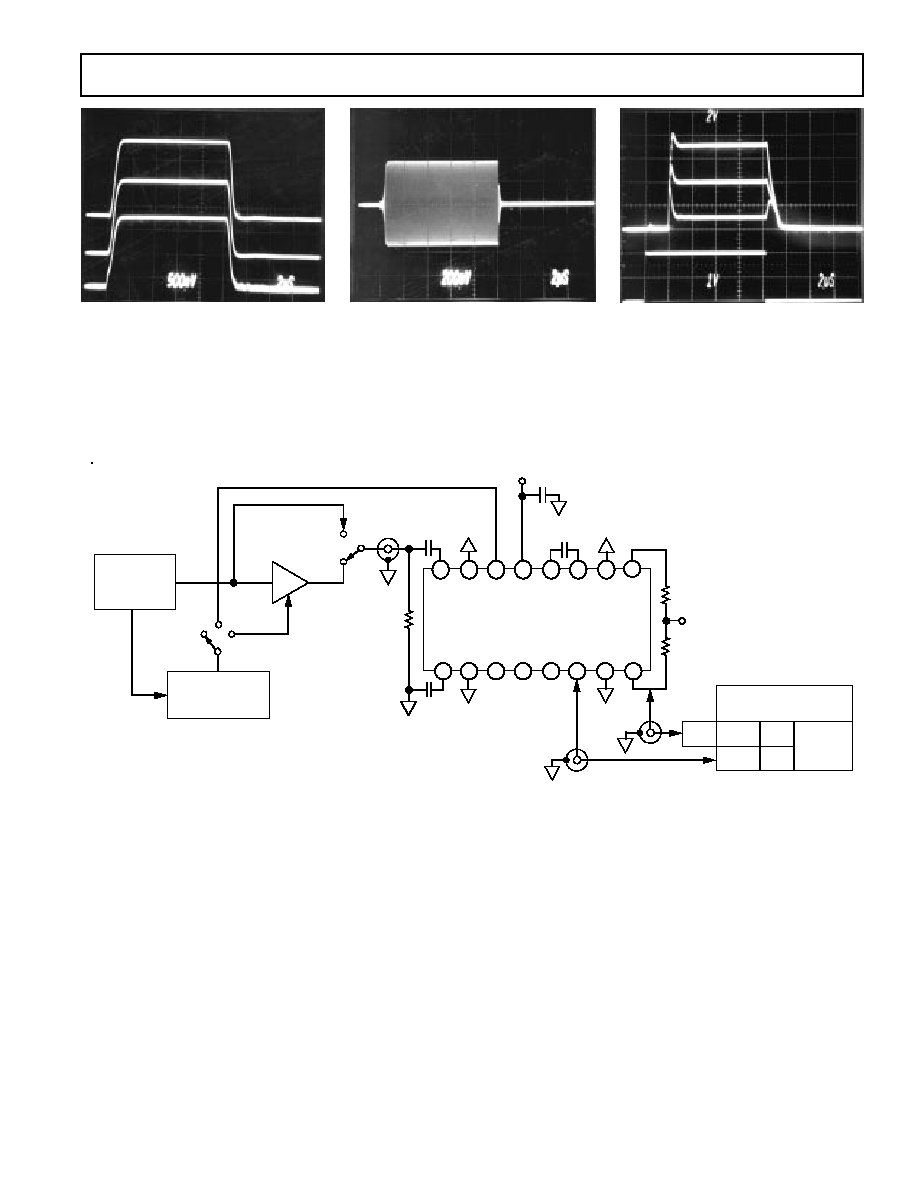
Power-Up Interface
The AD606 features a power-saving mode, controlled by the
logic level at Pin 14 (PRUP). When powered down, the quies-
cent current is typically 65
µ
A, or about 325
µ
W. A CMOS logi-
cal HIGH applied to PRUP activates both internal references,
and the system becomes fully functional within about
3.5
µ
s. When this input is a CMOS logical LOW, the system
shuts down to the quiescent level within about 5
µ
s.
The power-up time is somewhat dependent on the signal level
and can be degraded by mismatch of the input coupling capaci-
tors. The explanation is as follows. When the AD606 makes the
transition from powered-down to fully active, the dc bias voltage
at the input nodes INHI and INLO (about +2.5 V) inevitably
changes slightly, as base current in the input transistors flows in
the bias resistors. In fact, first-order correction for this is in-
cluded in the specially designed offset buffer amplifier, but even
a few millivolts of change at these inputs represents a significant
equivalent "dBm" level.
Now, if the coupling capacitors do not match exactly, some
fractional part of this residual voltage step becomes coupled into
the amplifier. For example, if there is a 10% capacitor mis-
match, and INHI and INLO jump 20 mV at power-up, there is
a 2 mV pulse input to the system, which may cause the offset
control loop to ring. Note that 2 mV is roughly 40 times greater
than the amplitude of a sinusoidal input at 75 dBm. As long as
the ringing persists, the AD606 will be "blind" to the actual in-
put, and V
LOG
will show major disturbances.
The solution to this problem is first, to ensure that the loop fil-
ter does not ring, and second, to use well-matched capacitors at
the signal input. Use the component values suggested above to
minimize ringing.
APPLICATIONS
Note that the AD606 has more than 70 MHz of input band-
width and 90 dB of gain! Careful shielding is needed to realize
its full dynamic range, since nearly all application sites will be
pervaded by many kinds of interference, radio and TV stations,
etc., all of which the AD606 faithfully hears. In bench evalua-
tion, we recommend placing all of the components in a shielded
box and using feedthrough decoupling networks for the supply
voltage. In many applications, the AD606's low power drain al-
lows the use of a 6 V battery inside the box.
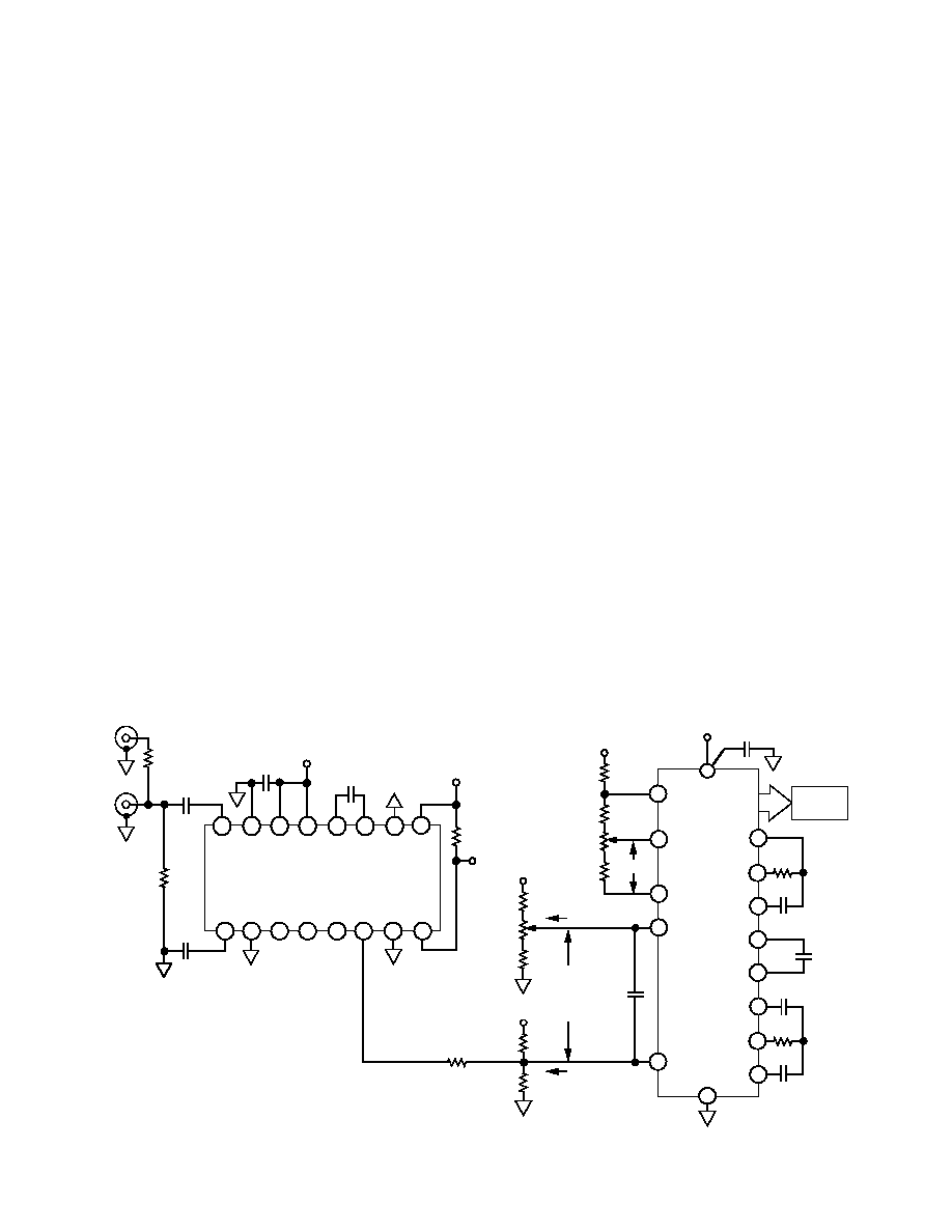
Basic RSSI Application
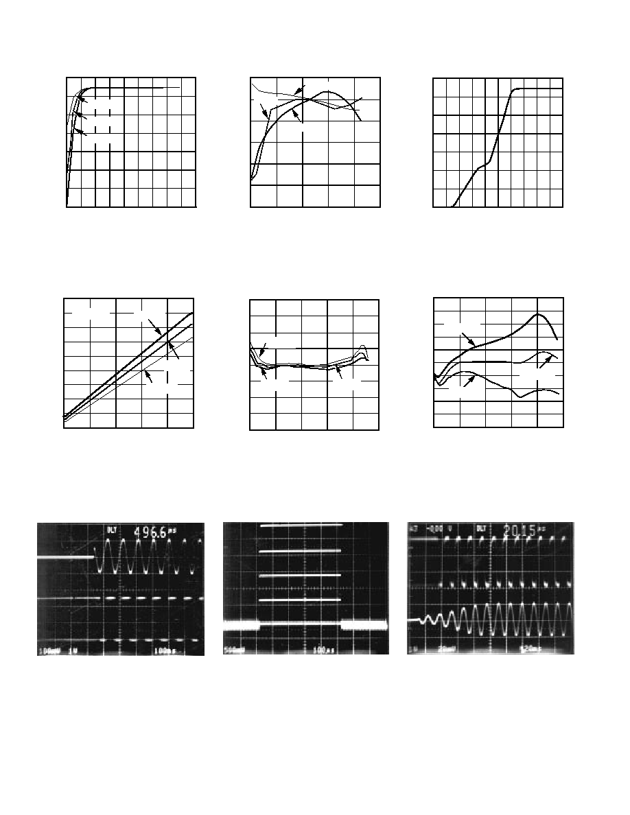
Figure 6 shows the basic RSSI (Receiver Signal Strength Indica-
tor) application circuit, including the calibration adjustments,
either or both of which may be omitted in noncritical applica-
tions. This circuit may be used "as is" in such measurement ap-
plications as the log/IF strip in a spectrum or network analyzer
or, with the addition of an FM or QPSK demodulator fed by the
limiter outputs, as an IF strip in such communications applica-
tions as a GSM digital mobile radio or FM receiver.
The slope adjustment works in this way: the buffer amplifier
(which forms part of a Sallen-Key two-pole filter, see Figure 2)
has a dc gain of plus two, and the resistance from BFIN (buffer
in) to OPCM (output common) is nominally 9.375 k
. This
resistance is driven from the logarithmic detector sections with a
current scaled 2
µ
A/dB, generating 18.75 mV/dB at BFIN,
hence 37.5 mV/dB at V
LOG
Now, a resistor (R4 in Figure 6)
connected directly between BFIN and VLOG would form a
controlled positive-feedback network with the internal 9.375 k
resistor which would raise the gain, and thus increase the slope
voltage, while the same external resistor connected between
BFIN and ground would form a shunt across the internal resis-
tor and reduce the slope voltage. By connecting R4 to a potenti-
ometer R2 across the output, the slope may be adjusted either
way; the value for R4 shown in Figure 6 provides approximately
±
10% range, with essentially no effect on the slope at the
midposition.
The intercept may be adjusted by adding a small current into
BFIN via R1 and R3. The AD606 is designed to have the nomi-
nal intercept value of 88 dBm when R1 is centered using this
network, which provides a range of
±
5 dB.
R4
174k
R3
412k
+5V
R2
50k
SLOPE
ADJUSTMENT
±
10%
RF INPUT
100pF
100pF
0.1
µ
F
R5
200
R1
200k
INTERCEPT
ADJUSTMENT
±
5dB
LIMITER OUTPUT
LOGARITHMIC
OUTPUT
+5V
7
8
1
2
3
4
5
6
9
10
15
16
14
13
INLO
VLOG
ILOG
ISUM
COMM
BFIN
OPCM
LMLO
LMHI
FIL2
FIL1
VPOS
PRUP
COMM
INHI
LADJ
12
11
AD606
51.1
NC
NC
Figure 6. Basic Application Circuit Showing Optional Slope and Intercept Adjustments
AD606
REV. 0
8
Adjustment Procedure
The slope and intercept adjustments interact; this can be mini-
mized by reducing the resistance of R1 and R2, chosen here to
minimize power drain. Calibration can be achieved in several
ways: The simplest is to apply an RF input at the desired oper-
ating frequency which is amplitude modulated at a relatively
low frequency (say 1 kHz to 10 kHz) to a known modulation in-
dex. Thus, one might choose a ratio of 2 between the maximum
and minimum levels of the RF amplitude, corresponding to a
6 dB (strictly, 6.02 dB) change in input level. The average RF
level should be set to about 35 dBm (the midpoint of the
AD606's range). R2 is then adjusted so that the 6 dB input
change results in the desired output voltage change, for ex-
ample, 226 mV at 37.5 mV/dB.
A better choice would be a 4:1 ratio (12.04 dB), to spread the
residual error out over a larger segment of the whole transfer
function. If a pulsed RF generator is available, the decibel incre-
ment might be enlarged to 20 dB or more. Using just a fixed-
level RF generator, the procedure is more time consuming, but
is carried out in just the same way: manually change the level by
a known number of decibels and adjust R2 until V
LOG
varies by
the corresponding voltage.
Having adjusted the slope, the intercept may now be simply ad-
justed using a known input level. A value of 35 dBm (397.6
mV rms, or 400 mV to within 0.05 dB) is recommended, and if
the standard scaling is used (P
X
= 88.33 dBm, V
Y
= 37.5 mV/
dB), then V
LOG
should be set to +2 V at this input level.
A Low Cost Audio Through RF Power Meter
Figure 7 shows a simple power meter that uses the AD606 and
an ICL7136 3-1/2 digit DMM IC driving an LCD readout. The
circuit operates from a single +5 V supply and provides direct
readout in dBm, with a resolution of 0.1 dBm.
In contrast to the limited dynamic range of the diode and
thermistor-styled sensors used in power meters, the AD606 can
measure signals from below 80 dBm to over +10 dBm. An op-
tional 50
termination is included in the figure; this could form
the lower arm of an external attenuator to accommodate larger
signal levels. By the simple expedient of using a 13 dB attenua-
tor, the LCD reading now becomes dBV (decibels above 1 V
rms). This requires a series resistor of 174
, presenting an
input resistance of 224
. Alternatively, the input resistance can
be raised to 600
using 464
and 133
. It is important to
note that the AD606 inputs must be ac coupled. To extend the
low frequency range, use larger coupling capacitors and an
external loop filter, as outlined earlier.
The nominal 0.5 V to 3.5 V output of the AD606 (for a 75 dBm
to +5 dBm input) must be scaled and level shifted to fit within
the +1 V to +4.5 V common-mode range of the ICL7136 for
the +5 V supply used. This is achieved by the passive resistor
network of R1, R2, and R3 in conjunction with the bias net-
works of R4 through R7, which provide the ICL7136 with its
reference voltage, and R9 through R11, which set the intercept.
The ICL7136 measures the differential voltage between IN HI
and IN LO, which ranges from 75 mV to +5 mV for a
75 dBm to +5 dBm input.
To calibrate the power meter, first adjust R6 for 100 mV be-
tween REF HI and REF LO. This sets the initial slope. Then
adjust R10 to set IN LO 80 mV higher than IN HI. This sets
the initial intercept. The slope and intercept may now be
adjusted using a calibrated signal generator as outlined in the
previous section.
To extend the low frequency limit of the system to audio fre-
quencies, simply change C1, C2, and C3 to 4.7
µ
F.
The limiter output of the AD606 may be used to drive the high-
impedance input of a frequency counter.
C4
1
µ
F
R1
1M
dBm
INPUT
C1
*
100pF
C2
*
100pF
0.1
µ
F
200
+5V
7
8
1
2
3
4
5
6
9
10
15
16
14
13
INLO
VLOG
ILOG
ISUM
COMM
BFIN
OPCM
LMLO
LMHI
FIL2
FIL1
VPOS
PRUP
COMM
INHI
LADJ
12
11
AD606JN
51.1
174
dBV
INPUT
C3
*
150pF
OPTIONAL
DRIVE TO
FREQUENCY
COUNTER
+5V
R9
5k
R8
100k
R10
100k
R2
54.9k
+5V
R3
54.9k
ICL7136CPL
V
26
0.1
µ
F
33
34
180k
50pF
40
39
38
1.8M
0.1
µ
F
0.047
µ
F
27
28
29
75.0
DISPLAY
+5V
1
0.1
µ
F
IN HI
IN LO
30
31
COMMON
REF LO
REF HI
36
35
32
R4
4.99k
+5V
R5
4.32k
R6
500
R7
162
100mV
2.513V NOM
80mV
FOR
0 dBm
SIGNAL
INPUT
2.433V NOM
+5V
NC
NC
NC
*
FOR AUDIO MEASUREMENTS CHANGE
C1, C2, AND C3 TO 4.7
µ
F; POSITIVE POLARITY
CONNECT TO PINS 1, 16
Figure 7. A Low Cost RF Power Meter
AD606
REV. 0
9
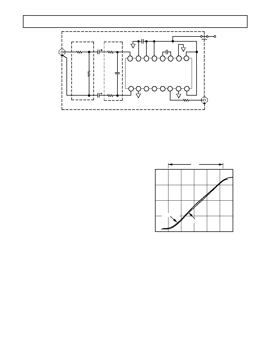
Low Frequency Applications
With reasonably sized input coupling capacitors and an optional
input low-pass filter, the AD606 can operate to frequencies as
low as 200 Hz with good log conformance. Figure 8 shows the
schematic, with the low-pass filter included in the dashed box.
This circuit should be built inside a die cast box and the signal
brought in through a coaxial connector. The circuit must also
have a low-pass filter to reject the attenuated RF signals that
would otherwise be rectified along with the desired signal and
be added to the log output. The shielded and filtered circuit has
a 90 dB dynamic range, as shown in Figure 9.
In this circuit, R4 and R5 form a 20 dB attenuator that extends
the input range to 10 V rms. R3 isolates loads from VLOG. Ca-
pacitors C1 and C2 (4.7
µ
F each), R1, R2, and the AD606's in-
put resistance of 2.5 k
form a 100 Hz high-pass filter that is
before the AD606; the corner frequency of this filter must be
well below the lowest frequency of interest. In addition, the
offset-correction loop introduces another pole at low signal lev-
els that is transformed into another high-pass filter because it is
in a feedback path. This indicates that there has to be a gradual
transition from a 40 dB roll off at low signal levels to a 20 dB
roll off at high signal levels, at which point the feedback low
pass filter is effectively disabled since the incoming signal
swamps the feedback signal.
This low-pass filter introduces some attenuation due to R1 and
R2 in conjunction with the 2.5 k
input resistance of the
AD606. To minimize this effect, the value of R1 and R2 should
be kept as small as possible100
is a good value since it bal-
ances the need to reduce the attenuation as mentioned above
with the requirement for R1 and R2 to be much larger then the
impedance of C1 and C2 at the low-pass corner frequency, in
our case about 1 MHz.
4
80
40
3
1
60
2
0
20
20
40
INPUT SIGNAL dBm
VLOG Volts DC
0
1kHz 10MHz
100Hz
90dB
3.5V
Figure 9. Performance of Low Frequency Circuit at 100 Hz
and 1 kHz to 10 MHz (Note Attenuation)
R3
1k
C4
4.7
µ
F
TO
DVM
0.1
µ
F
+5V
7
8
1
2
3
4
5
6
9
10
15
16
14
13
INLO
VLOG
ILOG
ISUM
COMM
BFIN
OPCM
LMLO
LMHI
FIL2
FIL1
VPOS
PRUP
COMM
INHI
LADJ
12
11
AD606JN
NC
NC
NC
R5
51.1
AC
INPUT
C1
4.7
µ
F
C2
4.7
µ
F
R1
100
R2
100
C3
680pF
R4
453
LOW-PASS
FILTER
DIECAST BOX
20dB
ATTENUATOR
Figure 8. Circuit for Low Frequency Measurements
REV. 0
10
AD606Typical Characteristics
5
25
20
10
20
60
15
80
0
5
0
20
40
INPUT LEVEL dBm
NORMALIZED PHASE SHIFT Degrees
10.7MHz
45MHz
70MHz
Figure 11. Normalized Limiter
Phase Response vs. Input Level at
10.7 MHz, 45 MHz, and 70 MHz
10
2
4
60
3
80
1
1
0
2
3
4
0
40
20
INPUT AMPLITUDE dBm
LOGARITHMIC ERROR dB
T
A
= 25
°
T
A
= +25
°
T
A
= +70
°
Figure 14. Logarithmic Conform-
ance as a Function of Input Level at
10.7 MHz at 25
°
C, +25
°
C, and
+70
°
C
Figure 17. V
LOG
Response to a
10.7 MHz CW Signal Modulated by
a 25
µ
s Wide Pulse with a 25 kHz
Repetition Rate Using 200 pF Input
Coupling Capacitors. The Input Sig-
nal Goes from +5 dBm to 75 dBm
in 20 dB Steps.
NORMALIZED LIMITER OUTPUT dB
INPUT LEVEL dBm
0.5
6.5
10
3.5
5.5
70
4.5
80
0.5
2.5
1.5
0
10
20
30
40
50
60
10.7MHz
45MHz
70MHz
Figure 10. Normalized Limiter
Amplitude Response vs. Input Level
at 10.7 MHz, 45 MHz and 70 MHz
4.5
0
+10
1
.5
60
80
2
1.5
2.5
3
3.5
4
0
20
40
INPUT POWER dBm
V
LOG
Volts DC
T
A
= +25
°
C
V
S
= 4.5V
V
S
= 5.5V
V
S
= 5V
Figure 13. V
LOG
Plotted vs. Input
Level at 10.7 MHz as a Function of
Power Supply Voltage
Figure 16. Limiter Response at
Onset of 10.7 MHz Modulated Pulse
at 75 dBm Using 200 pF Input
Coupling Capacitors
PRUP VOLTAGE Volts
POWER SUPPLY CURRENT mA
14
0
5
6
2
0.5
4
0
12
8
10
4.5
4
3.5
3
2.5
2
1.5
1
Figure 12. Supply Current vs. PRUP
Voltage at +25
°
C
T
A
= +25
°
C
T
A
= +70
°
C
5
5
10
2
4
60
3
80
1
1
0
2
3
4
0
40
20
INPUT AMPLITUDE dBm
LOGARITHMIC ERROR dB
T
A
= 25
°
C
Figure 15. Logarithmic Conform-
ance as a Function of Input Level at
45 MHz at 25
°
C, +25
°
C, and +70
°
C
Figure 18. Limiter Response at
Onset of 70 MHz Modulated Pulse
at 55 dBm Using 200 pF Input
Coupling Capacitors
AD606
REV. 0
11
Figure 19. V
LOG
Output for a Pulsed
10.7 MHz Input; Top Trace:
35 dBm to +5 dBm; Middle Trace:
15 dBm to 55 dBm; Bottom
Trace: 35 dBm to 75 dBm
Figure 20. Example of Test Signal
Used for Figure 19
Figure 21. V
LOG
Output for
10.7 MHz CW Input with PRUP Tog-
gled ON and OFF; Top Trace:
+5 dBm Input; Middle Trace:
35 dBm Input; Bottom Trace:
75 dBm; PRUP Input from HP8112A:0
to 4 V, 10
µ
s Pulse Width with
10 kHz Repetition Rate
MODULATED
PULSE
TESTS
SWEPT-GAIN
TESTS
C1
100pF
C2
100pF
51.1
C3
150pF
+5V
NC
NC
NC
7
8
1
2
3
4
5
6
9
10
15
16
14
13
INL
O
VL
O
G
IL
O
G
IS
UM
CO
M
M
BF
IN
OP
C
M
LM
LO
LM
H
I
FI
L
2
FI
L1
VP
O
S
PR
UP
CO
M
M
INHI
LA
D
J
12
11
AD606JN
RF
INPUT
TEKTRONIX 7704A
MAINFRAME
OSCILLOSCOPE
7A18
AMP
P6201
PROBES
7B53A
TIME-BASE
6137
PROBES
7A24
AMP
10 x
ATTN
0.1
µ
F
+5V
AD602
10dB to +30dB
(10.7MHz SWEPT
GAIN TESTS ONLY)
FLUKE 6082A
SYNTHESIZED
SIGNAL
GENERATOR
HEWLETT PACKARD
8112A PULSE
GENERATOR
200
200
Figure 22. Test Setup for Characterization Data
AD606
REV. 0
12
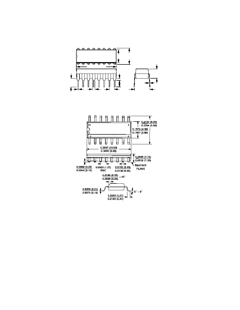
OUTLINE DIMENSIONS
Dimensions shown in inches and (mm).
16-Pin Plastic (N-16) Package
0.125
(3.18)
MIN
0.035
(0.89)
0.18
(4.57)
0.3 (7.62)
0.87 (22.1) MAX
0.25
(6.35)
0.31
(7.87)
0.18(4.57)
MAX
0.011
(0.28)
1
8
9
16
0.018 (0.46)
0.033 (0.84)
0.1 (2.54)
16-Pin Plastic Narrow-Body
Small Outline IC (R-16A) Package
PRINTED IN U.S.A.
C1698247/92