 | ÐлекÑÑоннÑй компоненÑ: AD6121ACP | СкаÑаÑÑ:  PDF PDF  ZIP ZIP |
Äîêóìåíòàöèÿ è îïèñàíèÿ www.docs.chipfind.ru
REV. B
Information furnished by Analog Devices is believed to be accurate and
reliable. However, no responsibility is assumed by Analog Devices for its
use, nor for any infringements of patents or other rights of third parties
which may result from its use. No license is granted by implication or
otherwise under any patent or patent rights of Analog Devices.
a
AD6121
One Technology Way, P.O. Box 9106, Norwood, MA 02062-9106, U.S.A.
Tel: 781/329-4700
World Wide Web Site: http://www.analog.com
Fax: 781/326-8703
© Analog Devices, Inc., 2000
CDMA 3 V Receiver IF Subsystem
with Integrated Voltage Regulator
FUNCTIONAL BLOCK DIAGRAM
2
I
Q
ROOFING
FILTER
IF
OUTPUT
DEMODULATOR
INPUT
IF AMPLIFIERS
INPUT STAGE
QUADRATURE DEMODULATOR
CDMA
INPUT
FM
INPUT
CDMA/FM
SELECT
GAIN
CONTROL
VOLTAGE
INPUT
1.23V
REFERENCE
OUTPUT
GAIN
CONTROL
VOLTAGE
REFERENCE
INPUT
POWER-
DOWN 2
POWER-
DOWN 1
IOUT
IOUT
QOUT
QOUT
LOCAL
OSCILLATOR
INPUT
VPOS
VREG
LOW
DROPOUT
REGULATOR
GAIN CONTROL
SCALE FACTOR
PTAT
TEMPERATURE
COMPENSATION
AD6121
FEATURES
Fully Compliant with IS98A and PCS Specifications
CDMA, W-CDMA, AMPS, and TACS Operation
Linear IF Amplifier
5.9 dB Noise Figure
47.5 dB to +47 dB Linear-in-dB Gain Control
Quadrature Demodulator
Demodulates IFs from 50 MHz to 350 MHz
Integral Low Dropout Regulator
200 mV Voltage Drop
Accepts 2.9 V to 4.2 V Input from Battery
Low Power
10 mA at Midgain
<1 A Sleep Mode Operation
Companion Transmitter IF Chip Available (AD6122)
APPLICATIONS
CDMA, W-CDMA, AMPS, and TACS Operation
QPSK Receivers
GENERAL DESCRIPTION
The AD6121 is a low power receiver IF subsystem specifically
designed for CDMA applications. It consists of high dynamic
range IF amplifiers with voltage controlled gain, a divide-by-two
quadrature generator, an I and Q demodulator, and a power-
down control input. An integral low dropout regulator allows
operation from battery voltages from 2.9 V to 4.2 V.
The gain control input accepts an external gain control voltage
input from a DAC. It provides 94.5 dB of gain control with a
nominal 52.5 dB/V scale factor when using an internal voltage
reference. The gain control interface reference input can be
connected to either the internal reference or an external reference.
The I and Q demodulator provides differential quadrature base-
band outputs to interface with CDMA baseband converters. A
divide-by-two quadrature generator followed by dual polyphase
filters ensures maximum
±2.5° quadrature accuracy.
The AD6121 IF Subsystem is fabricated using a 25 GHz f
t
BiCMOS silicon process and is packaged in a 28-lead SSOP
and a 32-leadless LPCC chip scale package (5 mm
× 5 mm).

2
REV. B
AD6121SPECIFICATIONS
(T
A
= +25 C, V
CC
= 3.0 V, LO = 2 IF, REFIN = 1.23 V, LDO Enabled, unless otherwise
noted) Note: All power measurements in dBm are referred to 1 k unless Z
IN
is noted.
Specification
Conditions
Min
Typ
Max
Units
TOTAL GAIN
Maximum Gain
IF Amplifiers and Demodulator Powered Up
+47
dB
IF Amplifiers Powered Up and Demodulator Powered Down
+41.4
dB
Minimum Gain
IF Amplifier and Demodulator Powered Up
47.5
dB
IF AMPLIFIER
CDMA and FM Input
IF = 85.38 MHz
Noise Figure
Maximum Gain
5.9
dB
Input Third-Order Intercept
Maximum Gain
42.8
dBm
Input 1 dB Compression Point
Maximum Gain
51.6
dBm
Gain Flatness
IF
±630 kHz, CDMA Mode
±0.25
dB
CDMA Input Capacitance
Differential
2.8
pF
CDMA Input Resistance
Differential
850
FM Input Capacitance
Differential
2.3
pF
FM Input Resistance
Differential
670
Output Capacitance
Differential
1.35
pF
Output Resistance
Differential
1.1
k
GAIN CONTROL INTERFACE
Gain Scaling
Using Internal Reference
52.5
dB/V
Gain Scaling Accuracy
Within a Gain Control Range of 90 dB
±3
dB/V
Gain Control Response Time
Minimum Gain to Maximum Gain
695
ns
Input Resistance at REFIN
10
M
Input Resistance at VGAIN
100
k
DEMODULATOR
LO = 172.76 MHz , 15 dBm Referred to 50
,
Baseband Frequency = 1 MHz
Differential Input Impedance
1
k
Differential Input Capacitance at
Demodulator Input
2.9
pF
Input Third Order Intercept
6.1
dBm
Demodulation Gain
5.6
dB
I/Q Output
Differential Output Voltage
10 k
, 2 pF Differential Parallel Load Impedance
700
mV p-p
Bandwidth
3 dB
16
MHz
Resistance
Single-Ended
630
Quadrature Accuracy
±2.5
Degree
Amplitude Balance
±0.1
±0.35 dB
LO Input Impedance
Differential
1.5
k
LO Input Capacitance
Differential
4.16
pF
CONTROL INTERFACES
Logic Threshold High
1.34
V
Logic Threshold Low
1.30
V
Input Current for Logic High
0.1
µA
Mode Control Response Time
CDMA/FM Pin High Selects CDMA, Low Selects FM
430
ns
Turn-On Response Time
PD1 and PD2 Pins Low Select IC ON, High Selects IC OFF
2.8
µs
Turn-Off Response Time
To 200
µA Supply Current
6.8
µs
LOW DROPOUT REGULATOR
External PNP Pass Transistor, VCE
SAT
= 0.4 V Max
h
FE
= 100/300 Min/Max
Input Range
2.9
4.2
V
Nominal Output
2.70
V
Voltage Drop
200
mV
Reference Output
1.23
V
POWER SUPPLY
Supply Range Using Internal LDO
Supply Input at Pin LDOE
2.95.0
V
Supply Range Bypassing Internal LDO
Supply Input at Pins DVCC, IFVCC, LDOC
2.73.6
V
Supply Current
VGAIN = 1.5 V
10
mA
Standby Current
0.78
µA
OPERATING TEMPERATURE
T
MIN
to T
MAX
40
+85
°C
Specifications subject to change without notice.
AD6121
3
REV. B
ABSOLUTE MAXIMUM RATINGS
1
Supply Voltage VPS1, VPS2 to COM1, COM2 . . . . . . . +5 V
Internal Power Dissipation
2
. . . . . . . . . . . . . . . . . . . 600 mW
Operating Temperature Range . . . . . . . . . . . 40
°C to +85°C
Storage Temperature Range . . . . . . . . . . . . 65
°C to +150°C
Lead Temperature Range (Soldering 60 sec) . . . . . . . . +300
°C
ORDERING GUIDE
Temperature
Package
Package
Model
Range
Description
Option
AD6121ARS
40
°C to +85°C
Shrink Small Outline Package (SSOP)
RS-28
AD6121ARSRL
40
°C to +85°C
28-Lead SSOP on Tape and Reel
AD6121ACP
40
°C to +85°C
Chip Scale Package (LPCC)
CP-32
AD6121ACPRL
40
°C to +85°C
32-Leadless LPCC on Tape and Reel
CAUTION
ESD (electrostatic discharge) sensitive device. Electrostatic charges as high as 4000 V readily
accumulate on the human body and test equipment and can discharge without detection.
Although the AD6121 features proprietary ESD protection circuitry, permanent damage may
occur on devices subjected to high-energy electrostatic discharges. Therefore, proper ESD
precautions are recommended to avoid performance degradation or loss of functionality.
WARNING!
ESD SENSITIVE DEVICE
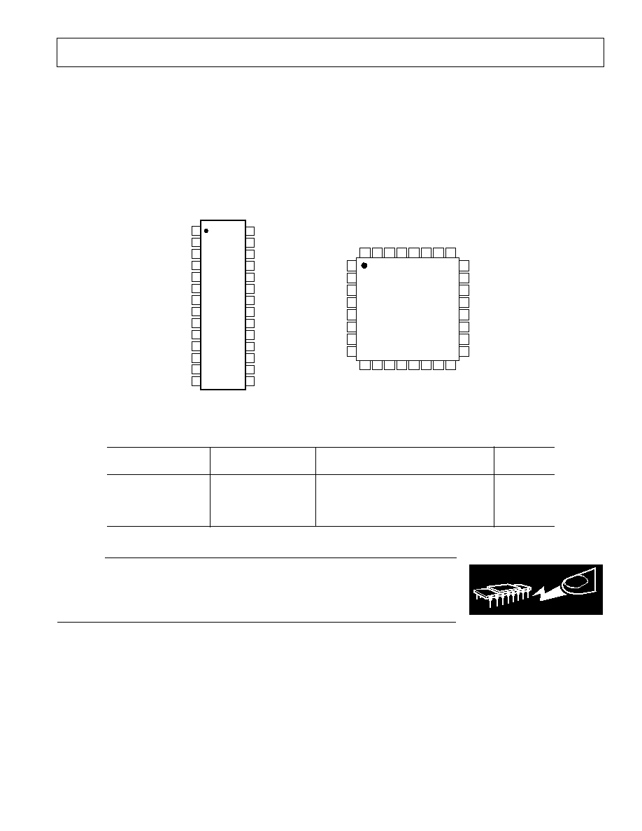
PIN CONFIGURATION
2
23
IFGND
LDOGND
3
22
FMIPP
IOPP
4
21
FMIPN
IOPN
5
20
IFVCC
QOPP
6
19
DGND
QOPN
7
18
LOIPP
PD1
8
17
LOIPN
REFOUT
1
24
IFGND
LDOGND
10
31
11
30
12
29
13
28
14
27
15
26
16
25
DVCC
CDMAIPP
LDOC
CDMA/FM
LDOB
IFOPP
LDOE
IFOPN
PD2
DEMIPN
VGAIN
DEMIPP
REFIN
NC
9
32
NC
CDMAIPN
AD6121 Top View
(Not to Scale)
TOP VIEW
(Not to Scale)
28
27
26
25
24
23
22
21
20
19
18
17
16
15
1
2
3
4
5
6
7
8
9
10
11
12
13
14
AD6121
LDOE
LDOB
LDOC
DVCC
LOIPN
LOIPP
DGND
CDMA/FM
CDMAIPP
CDMAIPN
IFGND
IFVCC
FMIPN
FMIPP
PD2
VGAIN
REFIN
REFOUT
PD1
QOPN
QOPP
IFOPP
IFOPN
DEMIPN
DEMIPP
IOPN
IOPP
LDOGND
SSOP Package
LPCC Package
NC = NO CONNECT
NOTES
1
Stresses above those listed under Absolute Maximum Ratings may cause perma-
nent damage to the device. This is a stress rating only; functional operation of the
device at these or any other conditions above those indicated in the operational
section of this specification is not implied. Exposure to absolute maximum rating
conditions for extended periods may affect device reliability.
2
Thermal Characteristics: 28-lead SSOP Package:
JA
= 115.25
°C/W.

AD6121
4
REV. B
PIN FUNCTION DESCRIPTIONS
SSOP
LPCC
Pin
Pin
Number
Number
Pin Label
Description
Function
1
30
CDMA/FM
Selects CDMA or FM Input
CMOS-compatible; HIGH = CDMA, LOW = FM.
2
31
CDMAIPP
CDMA "Positive" Input
AC-coupled, IF input from CDMA SAW filter.
3
32
CDMAIPN
CDMA "Negative" Input
AC-coupled, IF input from CDMA SAW filter.
4
1, 2
IFGND
IF Ground
Ground.
5
3
FMIPP
FM "Positive" Input
AC-coupled, IF input from FM SAW filter.
6
4
FMIPN
FM "Negative" Input
AC-coupled, IF input from FM SAW filter.
7
5
IFVCC
IF VCC
VCC for IF AGC amplifiers.
8
6
DGND
Digital Ground
Ground.
9
7
LOIPP
Local Oscillator "Positive" Input
AC-coupled, Differential Local Oscillator Input.
10
8
LOIPN
Local Oscillator "Negative" Input AC-coupled, Differential Local Oscillator Input.
9, 25
NC
No Connect
11
10
DVCC
Digital VCC
VCC for control logic.
12
11
LDOC
Low Dropout Regulator Pass
Connects to collector of external PNP pass transistor.
Transistor Collector Connection
13
12
LDOB
Low Dropout Regulator Pass
Connects to base of external PNP pass transistor.
Transistor Base Connection
14
13
LDOE
Low Dropout Regulator Pass
Connects to emitter of external PNP pass transistor
Transistor Emitter Connection
and DVCC, IFVCC.
15
14
PD2
Demodulator Power-Down
Demodulator Power-Down Control Input CMOS-
Control Input
compatible; HIGH = Modulator Off, LOW = Modulator On.
16
15
VGAIN
Gain Control Voltage Input
Accepts gain control input voltage from external DAC.
Max Gain = 2.5 V. Min Gain = 0.5 V.
17
16
REFIN
Gain Control Reference Input
Accepts 1.23 V reference input from REFOUT (Pin 17)
or external reference.
18
17
REFOUT
Reference Output
Provides 1.23 V reference output to REFIN (Pin 18) and
CDMA baseband IC reference input so that gain control
DAC and AD6121 use same reference.
19
18
PD1
IF Amplifier Power-Down
IF Amplifier Power-Down Control Input, CMOS com-
Control Input
patible; HIGH = Entire IC Powers Down, LOW = IF
Amplifier On.
20
19
QOPN
Q Output "Negative"
Connects to Q "Negative" Input of baseband IC.
21
20
QOPP
Q Output "Positive"
Connects to Q "Positive" Input of baseband IC.
22
21
IOPN
I Output "Negative"
Connects to I "Negative" Input of baseband IC.
23
22
IOPP
I Output "Positive"
Connects to I "Positive" Input of baseband IC.
24
23, 24
LDOGND
Ground
Ground.
25
26
DEMIPP
Demodulator "Positive" IF Input
Demodulator input from roofing filter.
26
27
DEMIPN
Demodulator "Negative" IF Input
Demodulator input from roofing filter.
27
28
IFOPN
IF Amplifier "Negative" IF Output
IF output to roofing filter.
28
29
IFOPP
IF Amplifier "Positive" IF Output
IF output to roofing filter.
AD6121
5
REV. B
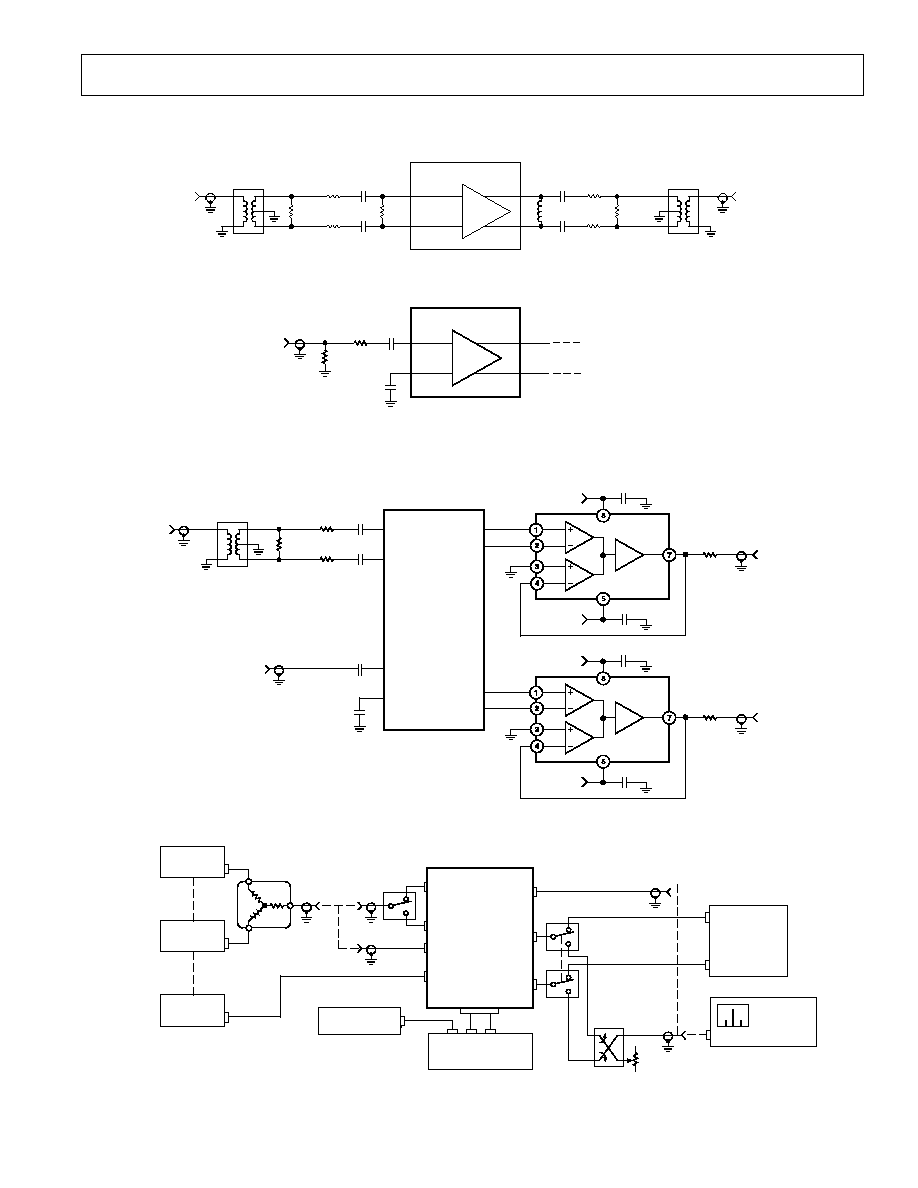
Test Figures
RF
SOURCE
1:8
909
110
110
10nF
1k
453
205
4:1
TO
SPECTRUM
ANALYZER
CDMAIPP
CDMAIPN
IFOPP
INDUCTOR CHOSEN FOR PEAK RESPONSE
AT THE TEST FREQUENCY (SEE TEXT)
IFOPN
AD6121
10nF
10nF
10nF
453
a. CDMA Input Port Characterization Impedance Match
50
10nF
IFOPP
IFOPN
AD6121
FMIPP
FMIPN
10nF
453
RF
SOURCE
b. FM Input Port Characterization Impedance Match
Figure 1. Quadrature Modulator Characterization Input and Output Impedance Matches
I CHANNEL
AD830
+15V
0.1 F
15V
OUT
Y2
Y1
X2
X1
A=1
50
V1
V1
V
P
V
N
0.1 F
10nF
205
453
453
Q CHANNEL
LO
SOURCE
10nF
RF
SOURCE
10nF
10nF
1:4
ALL SIGNAL PATHS MUST BE EQUAL
LENGTHS FOR I/Q MEASUREMENTS
AD830
+15V
0.1 F
15V
OUT
Y2
Y1
X2
X1
A=1
50
V1
V
P
V
N
0.1 F
V1
DEMIPP
DEMIPN
IOPP
IOPN
AD6121
QUADRATURE
DEMODULATOR
LOIPP
LOIPN
QOPP
QOPN
Figure 2. IF Amplifier Characterization Input and Output Impedance Matches
R&S FSEA
SPECTRUM
ANALYZER
RF INPUT
R & S
SMT03
RF
HP34970A
DATA ACQUISITION
& SWITCH CONTROL
ALL DC MEASUREMENT
AND CONTROL SIGNALS
SYNC
REFERENCE
SYNC
REFERENCE
50
TERMINATOR
HP8508A
VECTOR
VOLTMETER
CH1
CH2
R & S
SMT03
RF
R & S
SMT03
RF
IF OUT
CDMA
IN
FM IN
DEMOD
IN
LO
INPUT
I CHANNEL
Q CHANNEL
DC I/O
AD6121
HPE3610
POWER SUPPLY
Figure 3. General Test Set
AD6121
6
REV. B
NOISE
SOURCE
TO NOISE
FIGURE
METER
1:8
10nF
1k
450
205
4:1
CDMAIPP
CDMAIPN
IFOPP
INDUCTOR CHOSEN FOR PEAK RESPONSE
AT THE TEST FREQUENCY
IFOPN
AD6121
10nF
10nF
10nF
450
REACTIVE
CONJUGATE
MATCH
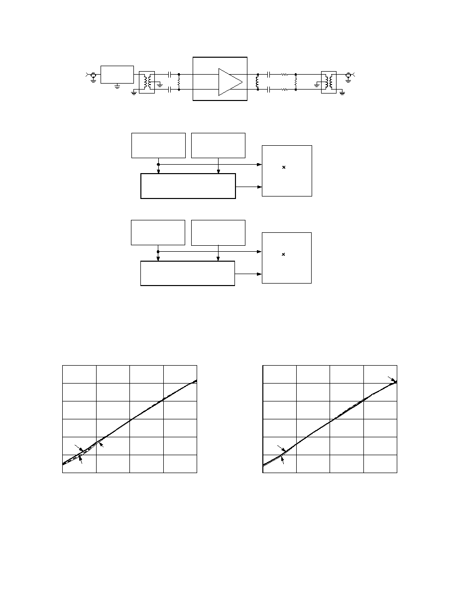
Figure 4. IF Amplifier Noise Figure Test Set
HP8116A
FUNCTION GEN
4kHz, 0.5V TO 2.5V
SQ WAVE
ROHDE & SCHWARZ
SMT03
80MHz, 50dBm
VGAIN
CDMA IN
IF OUT
TEKTRONIX
TDS 744A
CH 1
WITH 10 PROBE
CH 2
WITH COAX CABLE
50
AD6121
CHARACTERIZATION
BOARD
a. Response Time From Gain Control to IF Output
HP8116A
FUNCTION GEN
4kHz, 0V TO 2.7V
SQ WAVE
ROHDE & SCHWARZ
SMT03
80MHz, 50dBm
CDMA IN
IF OUT
TEKTRONIX
TDS 744A
CH 1
WITH 10 PROBE
CH 2
WITH COAX CABLE
50
AD6121
CHARACTERIZATION
BOARD
PD1, PD2
b. Response Time From PD1 and PD2 Control to IF Output
Figure 5. Response Time Setup
VGAIN Volts
60.00
40.00
0.5
2.5
1
GAIN
dB
1.5
2
0.00
20.00
40.00
60.00
20.00
T
A
= +85 C
T
A
= 40 C
T
A
= +25 C
Figure 6. IF Amplifier's Gain vs. VGAIN, IF = 70 MHz,
T
A
= 40
°C, +25°C and +85°C
VGAIN Volts
60.00
40.00
0.5
2.5
1
GAIN
dB
1.5
2
0.00
20.00
40.00
60.00
20.00
T
A
= +85 C
T
A
= 40 C
T
A
= +25 C
Figure 7. IF Amplifier's Gain vs. VGAIN, IF = 85 MHz,
T
A
= 40
°C, +25°C and +85°C
Typical Performance Characteristics
AD6121
7
REV. B
VGAIN Volts
40.00
0.5
2.5
1
GAIN
dB
1.5
2
0.00
20.00
60.00
20.00
T
A
= +85 C
T
A
= 40 C
T
A
= +25 C
40.00
Figure 8. IF Amplifier's Gain vs. VGAIN, IF = 210 MHz,
T
A
= 40
°C, +25°C and +85°C
VGAIN Volts
4.00
0
2.5
0.5
GAIN STEP ERROR
dB
1
1.5
2.00
2.50
1.00
3.50
1.50
3.00
0.50
0.00
2
T
A
= +85 C
T
A
= 40 C
T
A
= +25 C
Figure 9. IF Amplifier's Gain Error vs. VGAIN, T
A
= 40
°C,
+25
°C and +85°C
GAIN dB
0
60
20
40
IIP3
dBm
20
0
20
30
50
10
40
40
60
IF = 85MHz
IF = 210MHz
Figure 10. IF Amplifier's Input IP3 vs. Gain, IF = 85 MHz,
210 MHz, T
A
= +25
°C
FREQUENCY MHz
38.00
0
200
50
IIP3
dBm
100
150
40.00
42.00
250
300
36.00
44.00
34.00
32.00
30.00
46.00
48.00
50.00
Figure 11. IF Amplifier's Input IP3 vs. Frequency, VGAIN =
+2.5 V, T
A
= +25
°C
GAIN dB
25
10
0
NOISE FIGURE
dB
10
15
10
0
20
5
50
20
30
40
2.7VPOS
3.0VPOS
3.6VPOS
Figure 12. IF Amplifier Noise Figure vs. GAIN, IF= 85 MHz,
T
A
= +25
°C
GAIN dB
25
10
0
NOISE FIGURE
dB
10
15
10
0
20
5
50
20
30
40
2.7VPOS
3.0VPOS
3.6VPOS
Figure 13. IF Amplifier Noise Figure vs. GAIN,
IF= 210 MHz, T
A
= +25
°C
AD6121
8
REV. B
FREQUENCY MHz
50.00
0
200
50
MAXIMUM GAIN
dB
100
150
30.00
20.00
10.00
0.00
40.00
250
300
T
A
= 40 C
T
A
= +85 C
T
A
= +25 C
Figure 14. IF Amplifier Maximum Gain vs. Frequency,
T
A
= 40
°C, +25°C and +85°C
FREQUENCY MHz
60.00
0
200
GAIN
dB
100
20.00
0.00
60.00
40.00
20.00
300
40.00
VGAIN = +2.5V
VGAIN = +1.5V
VGAIN = +0.5V
Figure 15. IF Amplifier Gain vs. Frequency, VGAIN =
+0.5 V, +1.5 V and = +2.5 V
FREQUENCY MHz
46.00
0
200
50
P1dB
dBm
100
150
48.00
50.00
250
300
52.00
44.00
54.00
56.00
58.00
60.00
40.00
42.00
Figure 16. IF Amplifier 1 dB Compression Point vs. Fre-
quency, VGAIN = +2.5 V
VGAIN V
2
0.5
INPUT P1dB
dBm
1
1.5
30
2.5
40
20
50
60
10
Figure 17. IF Amplifier Input 1 dB Compression Point vs.
VGAIN, IF = 85.38 MHz
BASEBAND FREQUENCY MHz
6
0
10
GAIN
dB
5
3
0
2
15
1
4
5
T
A
= +85 C
T
A
= 40 C
T
A
= +25 C
Figure 18. Demodulator I Channel Gain vs. Baseband
Frequency, IF = 85 MHz
INTERMEDIATE FREQUENCY MHz
0
100
GAIN
dB
200
0
20
10
10
20
300
400
T
A
= 40 C
T
A
= +25 C
T
A
= +85 C
Figure 19. Demodulator I Channel Gain vs. IF, Baseband
Frequency = 1 MHz, T
A
= 40
°C, +25°C and +85°C
AD6121
9
REV. B
BASEBAND FREQUENCY MHz
0.25
0
5
AMPLITUDE BALANCE I
Q
dB
0.2
0.15
0
0.1
15
0.05
IF = 85MHz
0.3
10
IF = 210MHz
Figure 20. Demodulator I and Q Amplitude Balance vs.
Baseband Frequency, IF = 85 MHz and 210 MHz
BASEBAND FREQUENCY MHz
4
0
5
GAIN
dB
2
2
15
0
IF = 85MHz
6
10
IF = 210MHz
Figure 21. Demodulator I Channel Gain vs. Baseband
Frequency, IF = 85 MHz and 210 MHz
INTERMEDIATE FREQUENCY MHz
2.0
0
PHASE ERROR I
Q
Degrees
1.5
0
400
1.0
2.5
100
0.5
200
300
T
A
= +85 C
T
A
= +25 C
T
A
= 40 C
Figure 22. Demodulator Phase Error vs. IF, Baseband
Frequency = 1 MHz, T
A
= 40
°C, +25°C and +85°C
BASEBAND FREQUENCY MHz
2.0
0
5
PHASE ERROR
Degrees
1.5
0.5
15
1.0
2.5
10
T
A
= +25 C
T
A
= 40 C
T
A
= +85 C
Figure 23. Demodulator Phase Error vs. Baseband Fre-
quency, IF = 85 MHz, T
A
= 40
°C, +25°C and +85°C
INTERMEDIATE FREQUENCY MHz
0
0
IIP3
dBm
5
15
400
10
5
100
200
300
T
A
= +25 C
T
A
= +85 C
T
A
= 40 C
Figure 24. Demodulator Input IP3 vs. IF, Baseband Fre-
quency = 1 MHz, T
A
= 40
°C, +25°C and +85°C
REGULATOR INPUT VOLTAGE Volts
2
2
2.5
REGULATOR OUTPUT VOLTAGE
Volts
1
1
5
0
3
3
3.5
4
4.5
T
A
= +85 C
T
A
= +25 C
T
A
= 40 C
Figure 25. LDO Regulator Output Voltage vs. Input Volt-
age, T
A
= 40
°C, +25°C and +85°C
AD6121
10
REV. B
X-AMP is a trademark of Analog Devices, Inc.
THEORY OF OPERATION
The AD6121 consists of high dynamic range IF amplifiers with
voltage controlled gain, a divide-by-two quadrature generator,
an I and Q demodulator, a low dropout regulator and power-
down control inputs (Figure 27).
The AD6121 accommodates both the desired CDMA signal
and an interferer 42 dB larger--approximately 6 mV p-p for the
desired signal and 700 mV p-p for the interferer--as specified in
the CDMA system.
IF Amplifiers and Gain Control
The IF gain is provided by two sections: a CDMA or FM input
stage followed by three cascaded IF amplifiers. The CDMA and
FM input stages use differential, continuously-variable attenua-
tors based on Analog Devices' patented X-AMPTM topology.
These low noise attenuators consist of a differential R-2R ladder
network, linear interpolator, and a fixed gain amplifier. The
bulk of the IF gain is provided by three cascaded, wideband
2
I
Q
ROOFING
FILTER
IF
OUTPUT
DEMODULATOR
INPUT
IF AMPLIFIERS
INPUT STAGE
QUADRATURE DEMODULATOR
CDMA
INPUT
FM
INPUT
CDMA/FM
SELECT
GAIN
CONTROL
VOLTAGE
INPUT
1.23V
REFERENCE
OUTPUT
GAIN
CONTROL
VOLTAGE
REFERENCE
INPUT
POWER-
DOWN 2
POWER-
DOWN 1
IOUT
IOUT
QOUT
QOUT
LOCAL
OSCILLATOR
INPUT
VPOS
VREG
LOW
DROPOUT
REGULATOR
GAIN CONTROL
SCALE FACTOR
PTAT
TEMPERATURE
COMPENSATION
AD6121
Figure 27. Functional Block Diagram
VGAIN Volts
16
0.5
2.5
1
CURRENT CONSUMPTION
mA
1.5
2
8
10
4
14
T
A
= 40 C
T
A
= +25 C
6
12
2
0
T
A
= +85 C
Figure 26. Current Consumption vs. VGAIN, T
A
= 40
°C,
+25
°C and +85°C
amplifiers. The gain and input bandwidth of the AD6121 are
identical for both the FM and CDMA operating modes. When
the CDMA/FM pin is high, CDMA mode is enabled. When the
pin is low, FM mode is enabled.
The IF amplifiers operate in two different configurations, one
with the I and Q demodulator powered up and another with the
I and Q demodulator powered down. The I and Q demodulator
power setting is configured with pin PD2. The power-down
control is further discussed in the section of this data sheet
entitled Power-Down Control.
When the demodulator is powered up, the outputs of the IF
amplifiers are internally dc-biased and there is no need for exter-
nal pull-up inductors. A roofing filter is required (see section
entitled Roofing Filter in this data sheet) when using the IF
amplifiers with the I and Q demodulator powered up. Under
these conditions, the IF amplifiers and the low noise attenuator
input stage has +41.4 dB of gain.
When the I and Q demodulator is powered down, the IF ampli-
fiers have open collector outputs resulting in the need for pull-
up inductors. Under this configuration, and with the output of
the IF amplifiers loaded with 1 k
, the gain of the IF amplifiers
and low noise attenuator input stage is +47 dB. The pull-up
inductors should be chosen so that the parasitic capacitance
seen at the output of the IF amplifiers is resonated at the fre-
quency of interest. Figure 28 shows how to configure the pull-up
inductors at the output of the IF amplifiers. The 10 nF capaci-
tors are used for ac coupling.
In order to resonate the parasitic capacitors, rearrange Equation
1 to solve for L.
f
LC
PAR
0
1
2
=
(1)
where f
0
is the IF frequency in Hertz, C
PAR
is the total parasitic
capacitance in Farads, and L is the total shunt inductor value in
henrys.
AD6121
11
REV. B
AD6121
IFOPP
IFOPN
2C
PAR
2C
PAR
L/2
L/2
V
CC
10nF
10nF
10nF
Figure 28. IF Amplifiers' Output Configuration When
I and Q Demodulator Is Powered Down
In order to confirm whether the pull-up inductors have been
properly designed, sweep the IF frequency and view the output
of the IF amplifiers on a spectrum analyzer. If the inductor
value is correct, the signal should peak at the IF frequency.
The gain of the two amplifier sections (input stage followed by
amplifiers) changes sequentially for optimum signal-to-noise
ratio. For example, in CDMA mode, the gain of the CDMA
input amplifier first increases to maximum and then the gain of
the cascaded IF amplifiers increases to maximum. Likewise, when
decreasing gain, the gain of the cascaded amplifiers decreases to
minimum before the gain of the CDMA input amplifier.
The gain control circuits contain both temperature compensa-
tion circuitry and a choice of internal or external reference for
adjusting the gain scale factor. The gain control input accepts an
external gain control voltage from a DAC. It provides 94.5 dB
of gain control range with a nominal 52.5 dB/V scale factor.
Either an internal or external reference may be used to set the
gain control scale factor.
The external gain control input signal should be free of noise. In
a typical wireless application, it is recommended to filter this
signal in order to reduce the noise that results from the DAC
that generates it. A simple RC filter can be employed, but care
should be taken with its design. If too big a resistor is used, a
large voltage drop may occur across the resistor resulting in
lower gain than expected (as a result of a lower voltage reaching
the AD6121). An RC filter with a 1 kHz bandwidth, employing
a 1 k
resistor is appropriate. This results in a 150 nF capacitor.
The resulting circuit is shown in Figure 29.
AD6121
VGAIN
150nF
1k
FROM
BASEBAND
CONVERTER
100k
Figure 29. Gain Voltage Filtering
The AD6121's overall gain, expressed in decibels, is linear in
dB with respect to the automatic gain control (AGC) voltage,
VGAIN. Either REFOUT, or an external reference voltage
connected to REFIN, may be used to set the voltage range for
VGAIN. When the internal 1.23 V reference, REFOUT, is
connected to REFIN, VGAIN will control the AGC range when
it is typically set between 0.5 V and 2.5 V. Minimum gain oc-
curs at minimum voltage on VGAIN and maximum gain occurs
at maximum voltage on VGAIN. The maximum and minimum
gain will not change with a change in voltage at REFIN. Rather,
the slope of the gain curve will change as a result of a change in
the required range for VGAIN. Figure 30 shows the piecewise
linear approximation of the gain curve for the AD6121.
MAXIMUM
GAIN
MINIMUM
GAIN
VGAIN Volts
GAIN
V/V
Figure 30. Piecewise Linear Approximation for the
AD6121 Gain Curve
Because the minimum and maximum gains for the AD6121 are
constant, we can approximate the VGAIN range for a given
REFIN voltage by using Equation 2.
VGAIN
GAIN
MinGain
REFIN
MaxGain MinGain
REFIN
=
×
+
(
)
.
.
1 6
0 4
(2)
Where MaxGain is the maximum gain (+47 dB) in dB, MinGain
is the minimum gain (47.5 dB) in dB, REFIN is the reference
input voltage, in volts, VGAIN is the gain control voltage input,
in volts, and GAIN is the particular gain, in dB, we would have
for a given REFIN and VGAIN. Consequently, for any REFIN
we choose, we can calculate the VGAIN range by solving Equa-
tion 2 for VGAIN. For example, in order to determine the
VGAIN value for the maximum gain condition, given a 1.23 V
REFIN, we can solve Equation 2 for VGAIN by substituting
47 dB for GAIN and MaxGain, 47.5 dB for MinGain and
1.23 V for REFIN. VGAIN can then be calculated to be 2.46
V, or approximately 2.5 V. For the minimum gain condition,
we can determine the VGAIN value by substituting 47 dB for
MaxGain, 47.5 dB for Gain and MinGain and 1.23 V for
REFIN. VGAIN can then be calculated to be 0.492 V or ap-
proximately 0.5 V.
I and Q Demodulator
The I and Q demodulator provides differential quadrature base-
band outputs to CDMA baseband converters. The demodulator
provides 5.6 dB of voltage gain in addition to the gain provided
by the IF amplifier stage. The outputs of the I and Q demodula-
tor are filtered with a low-pass filter, which typically has a 16 MHz
bandwidth. A divide-by-two quadrature generator followed by
dual polyphase filters ensures a typical
±1° quadrature accuracy
(Figure 31).
2
180
POLYPHASE
FILTERS
I
Q
I
Q
2 IF
LO INPUT
QUADRATURE
OUTPUT TO
DEMODULATOR
2
Figure 31. Simplified Quadrature Generator Circuit
AD6121
12
REV. B
Power-Down Control
The AD6121 can operate with the IF amplifier and I and Q
demodulator stages both powered up, the IF amplifiers powered
up alone or both the IF amplifiers and demodulator powered
down. The AD6121 cannot operate with the demodulator pow-
ered up and the IF amplifiers powered down. The control for
these different modes is performed via the PD1 and PD2 pins.
Table I shows the decoding of the logic inputs.
Table I. AD6121 Operating Modes
PD1
PD2
IF Amplifiers
Demodulator
0
0
ON
ON
0
1
ON
OFF
1
0
INVALID STATE
INVALID STATE
1
1
OFF
OFF
Low Dropout Regulator
The AD6121 incorporates an integrated low dropout regulator.
The regulator accepts inputs from 2.9 V to 4.2 V and supplies
2.7 V at LDOC. The 2.7 V signal can be used to provide the dc
voltages required for the DVCC and IFVCC dc supplies. In order
to configure the low dropout regulator, an external pass transistor
is required. A pnp transistor with a minimum h
FE
of 100 and a
maximum h
FE
of 300 and a V
CE
(Sat.) of 0.4 V is required. In
order to use the low dropout regulator, configure the transistor
as shown in Figure 32. The 10 nF capacitor in Figure 32 is used
for decoupling the 2.7 V dc signal.
In addition to the low dropout regulator, there is a bandgap
voltage reference which produces a 1.23 V reference voltage at
pin REFOUT. This reference voltage will be present whenever a
voltage is applied to IFVCC and DVCC. This 1.23 V reference
voltage can then be used to provide the gain reference voltage
for the receive ADCs in the baseband converter.
AD6121
LDOC
LDOB
LDOE
REFOUT
1.23V
PASS
TRANSISTOR
2.7V
2.7V TO 4.2V
10nF
Figure 32.
Configuring the Low Dropout Regulator
It is possible to bypass the low dropout regulator on the AD6121
and use an external regulator instead. In order to bypass the
integrated low dropout regulator, connect pins LDOE, LDOB
and LDOC together and then connect them all to the external
regulator voltage. This configuration is shown in Figure 33.
Even when the low dropout regulator is bypassed, the 1.23 V
reference voltage at pin REFOUT is still present.
AD6121
LDOC
LDOB
LDOE
REFOUT
1.23V
FROM EXTERNAL
VOLTAGE
REGULATOR
Figure 33. Configuration for Bypassing the Low Dropout
Regulator
ROOFING FILTER
When the IF amplifiers and I and Q demodulator of the AD6121
are both powered up, the parasitic impedances seen at the out-
put of the IF amplifiers and inputs of the I and Q demodulator
are high enough to create a low-pass filter, which may attenuate
the IF signal. Consequently, the parasitic capacitance must be
cancelled by using an external inductor to form a parallel reso-
nant circuit. The external inductor that is required and the
internal parasitic capacitors form what is known as the roofing
filter, with the resonant frequency given by Equation 1 (see IF
Amplifiers and Gain Control section of this data sheet).
The roofing filter may be composed of a shunt inductor between
the IF amplifiers differential output pins. Because the demodu-
lator is powered up when the output of the IF amplifiers are fed
into the I and Q demodulator, the output of the IF amplifiers
are not open collector. As a result, pull up inductors are not
required. This configuration is shown in Figure 34. The 10 nF
capacitors are used for ac coupling.
L
AD6121
DEMIPP
DEMIPN
IFOPN
IFOPP
2C
PAR
2C
PAR
10nF
10nF
Figure 34. Roofing Filter Configuration
In order to confirm whether the roofing filter has been correctly
designed, sweep the IF frequency and view the output of the I
and Q demodulator on a spectrum analyzer. The output level
of the I or Q signal should be approximately flat from dc to
16 MHz, after which the low-pass filters at the I and Q output
will attenuate the signal. With the correct roofing filter induc-
tor, the I and Q output signal will be higher than for any other
roofing filter inductor value.
It should be noted that the roofing filter is only required when
cascading the output from the IF amplifiers to the input of the I
and Q demodulator. If we are looking at the output of the IF
amplifiers, no roofing filter is required. Because the IF amplifi-
ers' outputs are open collector when the I and Q demodulator is
powered down, pull-up inductors will be required in order to set
the dc voltage (see the section of this data sheet entitled IF
Amplifiers and Gain Control) and to resonate the parasitic
capacitors that are present under these conditions.
LEVEL DIAGRAM
Figure 35 is provided in order to better understand the different
voltage and power levels you can expect to see at different points
on the AD6121. It represents the levels that would be seen on
Rev. B of the AD6121 Customer Evaluation Board. When try-
ing to make these measurements, a high impedance (10 M
)
active FET probe (for example, the TEK P6204 from Tektronix)
should be used to minimize the effects of loading the circuits
with the probe.
AD6121
13
REV. B
IFVCC
DGND
LOIPP
LOIPN
DVCC
LDOC
LDOB
LDOE
IFOPP
IFOPN
DEMIPN
DEMIPP
IOPP
IOPN
PD1
REFOUT
REFIN
VGAIN
LDOGND
VCC
2
I
Q
CDMA/FM
LOW
DROPOUT
REGULATOR
GAIN
CONTROL
SCALE
FACTOR
AD6121
CDMAIPN
CDMAIPP
IFGND
FMIPN
FMIPP
QOPP
QOPN
PD2
TEMP
COMP
I INPUT POS
I INPUT NEG
Q INPUT POS
Q INPUT NEG
EXT REF IN
RX AGC DAC
CDMA
BASEBAND
IC
1k
159nF
Figure 36. Typical Application Showing Interface to Baseband IC with SSOP Package
50
50
8.55dBm
REFERRED TO 50
236mV p-p
5.55dBm
REFERRED TO 100
472mV p-p
AD830
SPECTRUM
ANALYZER
19.6dBm DIFFERENTIAL
REFERRED TO 700
247.8mV p-p DIFFERENTIAL
LOCAL
OSCILLATOR INPUT
168.76MHz
100mV p-p DIFFERENTIAL
Z
IN
= 500
V
GAIN
= 2.5V
GAIN = +41.4dB
Z
IN
= 700
AT 85.38MHz
14dBm DIFFERENTIAL
REFERRED TO 700
472mV p-p DIFFERENTIAL
f = 85.38MHz
61dBm DIFFERENTIAL
REFERRED TO 500
1.78mV p-p DIFFERENTIAL
f = 85.38MHz
60dBm
REFERRED TO 50
632.5mV p-p DIFFERENTIAL
2
I
Q
IOUT
IOUT
QOUT
QOUT
50
50
AD830
1:8
1k
SIGNAL
GENERATOR
50
Figure 35. AD6121 Signal Level Diagram for AD6121 Customer Sample Board, Rev. B
OUTPUT INTERFACES
The AD6121 interfaces to CDMA baseband converters requir-
ing either IF or baseband inputs. The baseband output is pro-
vided by direct connection of the AD6121's baseband output to
the baseband input of the baseband converter (Figure 36). The
output interfaces are controlled by the AD6121's power-down
modes.
AD6121 CUSTOMER EVALUATION BOARD
The AD6121 customer evaluation board consists of an AD6121,
I/O connectors, 3 two-pin headers, a 20-pin dual header and
two AD830 High Speed Video Difference Amplifiers. It allows
the user to evaluate the AD6121's I and Q demodulator and IF
amplifiers operating together or separately. The board is identical
for both the SSOP and LPCC packages. Because the AD6121 can
operate at any IF frequency from 50 MHz to 350 MHz, pads
are provided on the LOIPP, IFIP, CDMAIP and DMOD IN
inputs as well as the IF OUT output ports to allow the user to
add matching networks. The board is configured for an IF fre-
quency of 85.38 MHz when shipped.
The AD830s are used to provide differential to single ended
conversion for analysis of the differential I and Q outputs. As a
result, the output can be displayed on a spectrum analyzer or
other test equipment requiring a single ended input.
Prior to applying a CDMA or FM input signal, the appropriate
mode must be selected. FM mode will be selected by shorting
the two pins of the two pin header labeled FM/CDMA. Open
circuiting these two pins will select CDMA mode.
In order to test the power-down modes of the AD6121, locate
the bank of 3 two-pin headers on the evaluation board. In order
to have both the IF amplifiers and the I and Q demodulator
powered up, short circuit each of the two pins on the two pin
headers labeled PD1 and PD2. In order to power down the
demodulator and keep the IF amplifiers powered up, short
circuit the 2 pins on the header labeled PD1 and open circuit

AD6121
14
REV. B
the header labeled PD2. As described in Table I of this data
sheet, it is invalid to have PD1 open circuited and PD2 short
circuited. In order to power down the IF amplifiers and de-
modulator, open circuit both PD1 and PD2.
As shipped, the board is configured as follows:
1. J1 is open circuited and J2 is short circuited. This enables the
LDO regulator. In order to bypass the LDO regulator, short
circuit J1 and open circuit J2.
2. X18, X26, X25 and X23 are short circuited resulting in
the IF amplifiers' output being connected to the I and Q
demodulator's input.
3. L4, the roofing filter inductor is optimized for an IF fre-
quency of 85.38 MHz.
4. L2 and L3 are open circuited, although the components are
soldered on one pad of each set of solder pads.
In order to evaluate the IF amplifiers and I and Q demodulator
independent of each other, the roofing filter will have to be
removed from the circuit and the pull up inductors will have to
be added at the output of the IF amplifiers. When evaluating the
IF amplifiers alone, the I and Q demodulator should be pow-
ered down as described earlier in this section. The 470 nH pull
up inductors required for the 85.38 MHz IF frequency are
provided with the board, however, they will need to be soldered
down to pads L2 and L3. The roofing filter should be discon-
nected from the circuit and the output ports for the IF ampli-
fiers as well as the input ports for the I and Q demodulator
should be connected. This is accomplished by open circuiting
X18, X25, X26 and X33 and short circuiting X19, X21, X27
and X29.
Table II describes the high frequency signal connectors on the
AD6121 customer sample board.
Table II. Evaluation Board SMA Signal Connector Descriptions
Connector
Description
LOIPP
Local oscillator positive input at 2
× IF frequency
FMIP
FM signal input port. The differential to single
ended conversion performed on board by a balun.
Impedance matched to 50
for a 85.38 MHz IF
frequency.
CDMAIP
CDMA signal input port. The differential to single
ended conversion performed on board by a balun.
Impedance matched to 50
for a 85.38 MHz IF
frequency.
IF OUT
IF Amplifier output port. The differential to single
ended conversion performed on board by a balun.
Impedance matched to 50
for a 85.38 MHz IF
frequency.
DMOD IN
Demodulator input port. The differential to single
ended conversion performed on board by a balun.
Impedance matched to 50
for a 85.38 MHz IF
frequency.
I CH
I channel output port for the I and Q demodulator.
Q CH
Q channel output port for the I and
Q demodulator
Table III lists the connections for the 20-pin power supply
connector.
Table III. 20-Pin Power Supply Connection Information
Pin
Number
Function
1
VPOS for AD6121.
2.9 V4.2 V using the LDO Regulator.
2.7 V4.2 V bypassing the LDO Regulator.
2
VPOS for AD6121.
2.9 V4.2 V using the LDO Regulator.
2.7 V4.2 V bypassing the LDO Regulator.
3
Ground.
4
Ground.
5
Ground.
6
Ground.
7
Ground.
8
PD1. Connects to 2-pin header labeled PD1.
9
Ground.
10
PD2. Connects to 2-pin header labeled PD2.
11
Ground.
12
FM/CDMA. Selects FM or CDMA mode.
Connected to 2-pin header labeled FM/CDMA.
13
Ground.
14
REFOUT. 1.23 V output reference voltage from
Pin 18 on AD6121.
15
Ground.
16
VGAIN. Gain control voltage input. Connected to
Pin 16 on AD6121.
17
Ground.
18
V
REGOUT
. The 2.7 V output of the LDO regulator
when it is enabled. Connects to Pin 12 on AD6121.
19
15 V for AD830 Amplifier.
20
+15 V for AD830 Amplifier.
A schematic diagram of the evaluation board is shown in
Figure 37.
AD6121
15
REV. B
INDICATES A 50 TRACE
15V
V
POS
2.9V 4.2V
L1
470nH
R4
10k
R5
10k
R6
10k
V
REG IN
2.9V 4.2V
PD1
PD2
FM/CDMA
REFOUT
VGAIN 0.5V 2.5V
V
REGOUT
+15V
V
POS
P2
2
4
6
8
10
12
14
16
18
20
P1
1
3
5
7
9
11
13
15
17
19
PD1
PD2
FM/CDMA
C21
10nF
R9
0
C20
10nF
REFOUT
J5
0
C19
0.1 F
R8
50
C16
0.1 F
C17
0.1 F
SOIC
PACKAGE
R7
50
I CH
AD830
+15V
15V
OUT
Y2
Y1
X2
X1
A=1
V1
V
P
V
N
U2
C18
0.1 F
Q CH
FM/CDMA
Z = 500
C1
10nF
C2
10nF
X6
X5
0
X3
120nH
X1
CDMAIP
T1
1:8
X4
X7
0
R1
1k
FMIP
X15
X17
X16
0
LO IN
C6
0.01 F
C7
10nF
C9
10nF
DVCC
IFVCC
V
REGOUT
J1
J2
0
Q1
V
REG IN
FMMT4403CT-ND
PD2
PD1
1
2
3
4
5
6
7
8
9
10
11
12
13
14
28
27
26
25
24
23
22
21
20
19
18
17
16
15
AD6121
U1
CDMA/FM
CDMAIPP
CDMAIPN
IFGND
FMIPP
FMIPN
IFVCC
DGND
LOIPP
LOIPN
DVCC
LDOC
LDOB
LDOE
IFOPP
IFOPN
DEMIPN
DEMIPP
LDOGND
IOPP
IOIPN
QOPP
QOPN
PD1
REFOUT
REFIN
VGAIN
PD2
X2
0
C3
10nF
C4
10nF
X5
0
X10
150nH
X8
X11
X7
0
X13
1k
X9
0
L2
470nH
C23
10nF
V
REGOUT
T4
8:1
C14
10nF
C15
10nF
C12
10nF
C13
10nF
IF
OUT
DMOD
IN
X29
X28
X27
X26
0
L4
620nH
C23
X33
0
X22
4pF
X24
X30
180nH
X32
X31
68nH
X25
0
L3
470nH
C24
10nF
V
REGOUT
T2
1:8
X18
0
T3
8:1
X19
X20
X23
150nH
X21
V1
SOIC
PACKAGE
AD830
+15V
15V
OUT
Y2
Y1
X2
X1
A=1
V1
V
P
V
N
U3
V1
VGAIN
C5
18pF
R3
10
C11
10nF
V
REGOUT
IFVCC
C8
18pF
R2
10
C10
10nF
V
REGOUT
DVCC
Figure 37. Schematic Diagram of AD6121 Evaluation Board
AD6121
16
REV. B
C00945b.56/00 (rev. B)
PRINTED IN U.S.A.
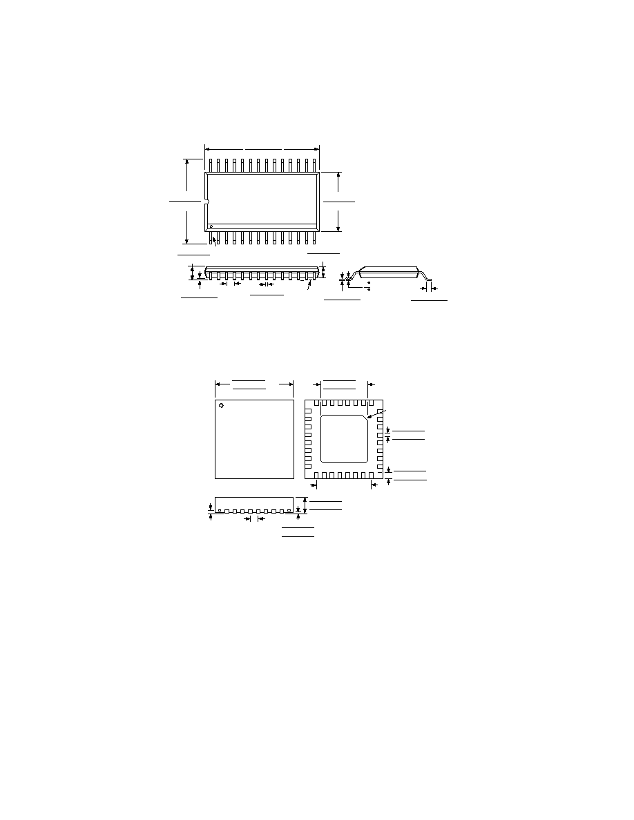
28-Lead Shrink Small Outline Package (SSOP)
(RS-28)
28
15
14
1
0.407 (10.34)
0.397 (10.08)
0.311 (7.9)
0.301 (7.64)
0.212 (5.38)
0.205 (5.21)
PIN 1
SEATING
PLANE
0.008 (0.203)
0.002 (0.050)
0.07 (1.79)
0.066 (1.67)
0.0256
(0.65)
BSC
0.078 (1.98)
0.068 (1.73)
0.015 (0.38)
0.010 (0.25)
0.009 (0.229)
0.005 (0.127)
0.03 (0.762)
0.022 (0.558)
8
0
32-Leadless Chip Scale Package (LPCC)
(CP-32)
1
32
9
8
17
BOTTOM
VIEW
25
24
16
0.018 (0.45)
0.016 (0.40)
0.014 (0.35)
0.138 (3.50) BSC
PIN 1
INDICATOR
0.015 (0.38)
0.012 (0.30)
0.009 (0.23)
0.128 (3.25)
0.106 (2.70) SQ
0.049 (1.25)
0.020 (0.50)
BSC
0.039 (1.00)
0.035 (0.90)
0.031 (0.80)
0.002 (0.05)
0.001 (0.02)
0.000 (0.00)
0.010
(0.25)
REF
0.205 (5.20)
0.197 (5.00) SQ
0.189 (4.80)
CONTROLLING DIMENSIONS ARE IN MILLIMETERS
DIMENSIONS MEET JEDEC MO-220-VHHD-2
OUTLINE DIMENSIONS
Dimensions shown in inches and (mm).