 | ÐлекÑÑоннÑй компоненÑ: AD6190 | СкаÑаÑÑ:  PDF PDF  ZIP ZIP |
Äîêóìåíòàöèÿ è îïèñàíèÿ www.docs.chipfind.ru
REV. 0
Information furnished by Analog Devices is believed to be accurate and
reliable. However, no responsibility is assumed by Analog Devices for its
use, nor for any infringements of patents or other rights of third parties
which may result from its use. No license is granted by implication or
otherwise under any patent or patent rights of Analog Devices.
a
AD6190
One Technology Way, P.O. Box 9106, Norwood, MA 02062-9106, U.S.A.
Tel: 781/329-4700
World Wide Web Site: http://www.analog.com
Fax: 781/326-8703
© Analog Devices, Inc., 1998
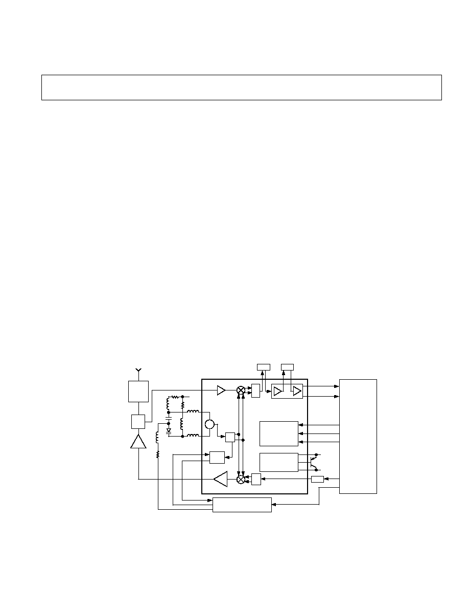
900 MHz RF Transceiver
FUNCTIONAL BLOCK DIAGRAM
/2
10.7
Z87L00
SPREAD-
SPECTRUM
CONTROLLER
T/R
S/W
ANT
FILTER
POWER
MANAGEMENT
AND
CONTROL
VOLTAGE
REGULATOR
0
90
PA
0
90
64/65
10.7
10.7
15MHz SYNTHESIZER
VREG
VBATT
LIMOUT
RSSI
TXON
RXON
VCOON
VREG
AD6190
I
Q
VCO
FEATURES
Complete 900 MHz RF Transceiver
LNA
Receive Mixer
Transmit Mixer
Driver Amplifier
VCO
Prescaler
Limiter Amplifier with RSSI
On-Chip Low Dropout Regulator
Independent Sleep Modes for TX, RX
28-Lead SSOP Package
APPLICATIONS
902 MHz928 MHz ISM Band Cordless Telephones
902 MHz928 MHz ISM Band Wireless Data Systems
GENERAL DESCRIPTION
The AD6190 900 MHz RF Transceiver provides a complete
RF/IF section for systems operating in the 902 MHz928 MHz
license-free ISM band. The high level of integration allows several
dozen discrete components to be replaced. It is ideally suited
for use in cordless telephone and wireless data applications.
The receiver section includes a Low Noise Amplifier (LNA).
The LNA's output drives an image-reject mixer; the mixer's
output optimized for 10.7 MHz is filtered and processed by the
limiting IF amplifier.
The transmit section accepts a modulated 10.7 MHz IF input,
and uses an image-reject upconverter to mix the signal up to the
902 MHz928 MHz RF carrier frequency while suppressing the
unwanted image and LO components. The RF output is raised
to a nominal 0.5 milliwatt (3 dBm) output level. This output
can be used directly or can drive an external power amplifier to
higher levels.
The on-chip VCO operates at 2
×
the local oscillator frequency.
This reduces oscillator pulling due to strong interferers in-band
or transmitter leakage. An on-chip 64/65 prescaler allows the
VCO to be controlled by a low cost 15 MHz CMOS synthesizer.
An on-chip low dropout regulator minimizes VCO pushing. The
transmit section, receive section, or both, can be placed in a low
current SLEEP mode when not in use. The AD6190 900 MHz
RF transceiver is packaged in a 28-lead SSOP package.
The AD6190 900 MHz RF Transceiver is part of the Analog
Devices/Zilog "A-to-Z Phone" Spread-Spectrum System for
cordless telephone and data communications applications. Con-
tact Zilog directly at (408) 370-8000 for more information on
the Z87000 series baseband controller chips.

2
REV. 0
AD6190SPECIFICATIONS
(@ T
A
= +25 C, V
CC
= +3.3 V, F
IF
= 10.7 MHz, F
RF
= 902 MHz928 MHz, TX IF Input
level 137 mV p-p, unless otherwise noted)
Parameter
Conditions
Min
Typ
Max
Units
RECEIVE RF SECTION
(LNA to Mixer Output)
Source Z = 50
, IF Load Z = 330
Power Gain
24
dB
Noise Figure
4.2
dB
1 dB Compression (Input)
30
dBm
Input IP3
17
dBm
Image Rejection
F
RF
= 915 MHz, F
LO
= 904.3 MHz
28
33
dBc
TRANSMIT UPCONVERTER
Image Rejection
F
IF
= 10.7 MHz, F
LO
= 904.3 MHz
35
48
dBc
LO Feedthrough
F
IF
= 10.7 MHz, F
LO
= 904.3 MHz
33
dBm
DRIVER AMPLIFIER
Nominal Output Power
For IF Input Level = 137 mV p-p
3
dBm
1 dB Compression
0
+4.5
dBm
VCO
Operating Frequency
(LO Frequency
×
2)
1783
1835
MHz
PRESCALER
Division Ratio
PREMOD = "1"
64
PREMOD = "0"
65
Output Level
R
L
= 2.2 k, C
L
< 10 pF
0.55
1.0
V p-p
IF LIMITER AMPLIFIER
First Stage Gain
24
dB
Second Stage Gain
70
dB
AC Output Level
R
L
> 30 k
, C
L
< 30 pF
450
mV p-p
DC Level
1.76
V
IF Port Impedance
F
IF
= 10.7 MHz
330
RSSI OUTPUT
Slope
With 10
in Series with VCCIF
22
mV/dB
Output Voltage
@ 100 dBm RF Input
0.90
V
@ 30 dBm RF Input
2.40
V
Linear Range
(With Respect to RF Input Level)
70
dB
RSSI Log Conformance Error
±
2
dB
SUPPLY CURRENT
(VCC = 3.3 V)
Transmit Mode
TXON, VCOON = 1; RXON = 0
93
mA
Receive Mode
RXON, VCOON = 1; TXON = 0
59
mA
Sleep Mode
TXON, VCOON, RXON = 0
270
µ
A
SUPPLY VOLTAGE
VBATT
3.0
4.6
V
Other Supplies
VCCTX, VCCIF, VCCLNA
3.0
3.3
3.6
V
VCO REGULATOR
Output Voltage, 3.0 < VBATT < 4.6 V
2.65
2.85
V
TEMPERATURE RANGE
20
+85
°
C
Specifications subject to change without notice.
AD6190
3
REV. 0
CAUTION
ESD (electrostatic discharge) sensitive device. Electrostatic charges as high as 4000 V readily
accumulate on the human body and test equipment and can discharge without detection.
Although the AD6190 features proprietary ESD protection circuitry, permanent damage
may occur on devices subjected to high energy electrostatic discharges. Therefore,
proper ESD precautions are recommended to avoid performance degradation or loss of
functionality.
ABSOLUTE MAXIMUM RATINGS
1
Supply Voltage
VBATT, VCCIF, LNAVCC, VCCTX to GND . . . . +5.5 V
Maximum RF Input Level Without Damage . . . . . . . +20 dBm
Internal Power Dissipation
2
. . . . . . . . . . . . . . . . . . . . 500 mW
Operating Temperature Range . . . . . . . . . . . 25
°
C to +85
°
C
Storage Temperature Range . . . . . . . . . . . . 65
°
C to +150
°
C
Lead Temperature Range
(Soldering, 60 sec) . . . . . . . . . . . . . . . . . . . . . . . . . . +300
°
C
ORDERING GUIDE
Model
Package Description
Package Option
AD6190ARS
28-Lead Shrink Small Outline
RS-28
AD6190ARSRL
28-Lead Shrink Small Outline, Supplied on Reels, 1500 Units per Reel
Minimum order quantity 25,000 units.
NOTES
1
Stresses above those listed under Absolute Maximum Ratings may cause perma-
nent damage to the device. This is a stress rating only; functional operation of the
device at these or any other conditions above those indicated in the operational
section of this specification is not implied. Exposure to absolute maximum rating
conditions for extended periods may affect device reliability.
2
Thermal Characteristics: 28-lead SSOP package
JA
= 122
°
C/W.
WARNING!
ESD SENSITIVE DEVICE
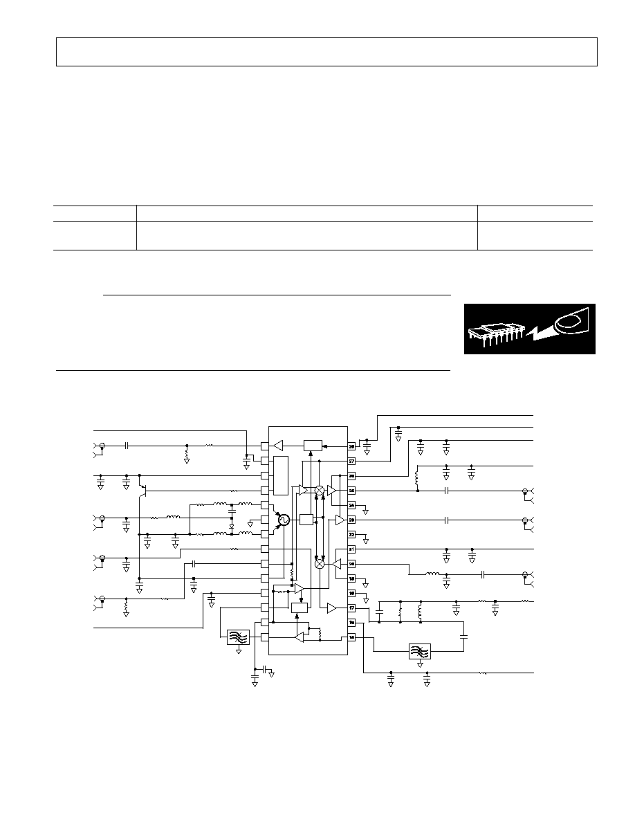
Figure 1. Test Circuit
AD6190
64/65
REG
2
RSSI
U1
1
2
3
4
5
6
7
8
9
10
11
12
13
14
82pF
10nF
82pF
82pF
10nF
220
301
54.9
82pF
82pF
0.1 F
82pF
0.1 F
82pF
15nH
15nH
15nH
220
1.96k
R3
51.1
Q1
82pF
1nF
VCOON
PRESCALER
OUT
TUNE
VOLTAGE IN
RSSI OUT
TRANSMIT
IF
IN
RXON
F1
82pF
82pF
10nF
8.2nH
82pF
10nF
2.2pF
82pF
100nF
TXON
VCCTX
(3.3VDC)
VCC DRIVER
(3.3VDC)
TRANSMIT
RF OUT
LIMITER OUT
VCCLNA
(3.3VDC)
15nH
82pF
2.2pF
LNA IN
6.8 H
(TDK2012)
6.8pF
1k
27pF
F1
10
82pF
100nF
39
VCC MIXER
(3.3VDC)
VCCIF
(3.3VDC)
10
100nF
82pF
82pF
10
2.75 VDC
IN
0.1 F
39
L1
L2
39
MODULUS CONTROL
VBATT
(3.0-4.5VDC)
C1
D1
AD6190
4
REV. 0
PIN FUNCTION DESCRIPTIONS
No.
Pin Name
Type
Function/Description
1
PREOUT
Output
Prescaler Output. Usually connected to input of external low frequency
CMOS synthesizer (Fujitsu MB87006A, Siemens PMB2307, or similar).
2
VCOON
Control
Logic "1" turns on power to VCO, and divider/prescalers.
3
VBATT
Power
VBATT connection for regulator. Normally connected to 3.3 V dc or battery.
4
VBASE
Power
Base connection to external regulator pass transistor (MMBT3906 or similar).
5
TANK
Input
Connection for VCO tank circuit (LC network).
6
GND
Power
Substrate ground connection.
7
TANK+
Input
Connection for VCO tank circuit (LC network).
8
RSSI
Output
Received Signal Strength Indicator output signal.
9
TXIF
Input
Accepts modulated transmit signal at 10.7 MHz IF.
10
VREG
Power
Regulated VCC for LO from external pass transistor.
11
RXON
Control
Logic "1" turns on power to LNA and receive mixer stages.
12
LIMIN
Input
Input to limiting amplifier.
13
IFAMPCOM
Input
Input signal common for limiting amplifier.
14
IFAMPOUT
Output
Output of first stage of IF amplifier. Normally connected through 10.7 MHz
filter to Pin 12 (LIMIN).
15
IFAMPIN
Input
Input to first stage of IF amplifier.
16
VCCIF
Power
Local VCC connection for IF amp/limiter stages.
17
RXMIXOUT
Output
10.7 MHz IF Output. Normally connected through 10.7 MHz filter to IF
amplifier input (Pin 15).
18
LNAGND
Power
Local ground for LNA.
19
GND
Power
Substrate ground connection.
20
RFIN
Input
LNA Input. Normally driven single-ended from 50
source impedance.
21
VCCLNA
Power
VCC for LNA.
22
GND
Power
Substrate ground connection.
23
LIMOUT
Output
10.7 MHz limiter output.
24
PAGND
Power
Local ground for PA stage emitter. Degeneration may be added.
25
RFOUT
Output
Transmitted RF output signal at 0 dBm level.
26
VCCTX
Power
Local VCC connection for TX stages.
27
TXON
Control
Logic "1" turns on power to transmit mixer, buffers, and PA stages.
28
PREMOD
Input
Prescaler Modulus control (HIGH = divide-by-64; LOW = divide-by-65).
PIN CONFIGURATION
PREOUT
RFOUT
VCCTX
TXON
PREMOD
VCOON
VBATT
VBASE
GND
LIMOUT
PAGND
TANK
GND
TANK+
RSSI
TXIF
VREG
LNAGND
RFIN
VCCLNA
RXON
LIMIN
IFAMPCOM
IFAMPOUT
LNAGND
IFAMPIN
VCCIF
RXMIXOUT
TOP VIEW
(Not to Scale)
28
27
26
25
24
23
22
21
20
19
18
17
16
15
1
2
3
4
5
6
7
8
9
10
11
12
13
14
AD6190
AD6190
5
REV. 0
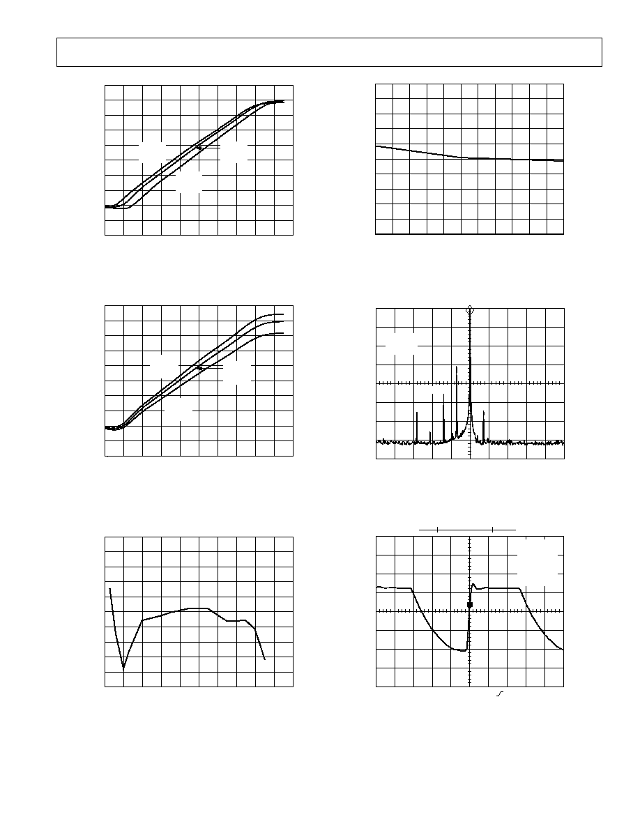
PIN dBm
2.5
1.0
0
115
15
105
RSSI Volts
95
85
75
65
55
45
35
25
2.25
1.25
0.75
0.25
1.75
1.5
0.5
2.0
3.3V
25 C
915MHz
3.3V
+25 C
915MHz
3.3V
+85 C
915MHz
Figure 2. RSSI Voltage vs. Input Power
PIN dBm
2.5
1.0
0
115
15
105
RSSI Volts
95
85
75
65
55
45
35
25
2.25
1.25
0.75
0.25
1.75
1.5
0.5
2.0
3.0V
+25 C
915MHz
3.3V
+25 C
915MHz
3.5V
+25 C
915MHz
Figure 3. RSSI Voltage vs. Input Power
PIN dBm
5.0
1.0
5.0
115
15
105
RSSI ERROR dB
95
85
75
65
55
45
35
25
4.0
0
2.0
4.0
2.0
1.0
3.0
3.0
Figure 4. RSSI Error vs. Input Power
TEMPERATURE C
1000
300
0
25
85
15
LIMITER V-p-p
5
5
15
25
35
45
55
65
75
900
400
200
100
800
600
700
500
Figure 5. Limiter Output Level vs. Temperature @ 3.3 V
and 915 MHz
CENTER 915.0 MHz
#RES BW 10 kHz
VBW 10 kHz
SPAN 150.0 MHz
SWP 4.50 sec
MARKER
915.0 MHz
0.0 dBm
L.O.
IMAGE
#AT 30 dB
MKR 915.0 MHz
0.0 dBm
Figure 6. Frequency Spectrum
Ch1 10.0mV
M 12.5ns Ch1
0V
Tek Run: 4.00GS/s ET Average
V: 72.0ns
@: 41.5ns
C1 Freq
13.899MHz
C1 +Duty
60.1%
T
[ ]
Figure 7. Prescaler Output
AD6190
6
REV. 0
PRODUCT DESCRIPTION
The AD6190 is a complete RF/IF transceiver for operation in
the 902 MHz928 MHz Industrial, Scientific and Medical
("ISM") frequency band. Together with a suitable spread-
spectrum controller, the AD6190 can be used to design
a spread-spectrum system compliant with FCC "Part 15"
(47CFR15.247) regulations. The AD6190 is a fully compatible
companion chip to the Zilog Z87L00 "ZPhone" frequency-
hopping spread-spectrum controller.
The AD6190 includes a receive path of LNA, image-reject
mixer, IF amplifier and limiter amplifier with RSSI. The trans-
mit path accepts a 10.7 MHz IF input signal, and uses image-
reject upconversion to the 902 MHz928 MHz band. Frequency
control is achieved using an on-chip VCO and dual-modulus
prescaler connected to an inexpensive low frequency PLL for
channel selection and frequency hopping.
Additionally, an on-chip voltage regulator stabilizes the VCO to
prevent LO pushing due to power supply variations.
APPLYING THE AD6190
Receive Signal Path
The AD6190 Low Noise Amplifier (LNA) and image-reject
mixer together provide downconverter with a total gain of 24 dB
and a typical Noise Figure (NF) of 4.2 dB.
The LNA input port exhibits an impedance of 320-j61 at
915 MHz. In order to provide an optimum match to a 50
source, the network shown in Figure 8 should be used.
RF IN
82pF
2.2pF
15nH
50
AD6190
Figure 8. LNA Input Matching Circuit
The frequency plan of the AD6190 provides the lowest possible
RF implementation cost. A single conversion design is used with
a 10.7 MHz IF to take advantage of the very low cost filters
available. However, since the 902 MHz928 MHz band is wider
than twice the IF, it is possible that undesired in-band signals
will be mixed down to the IF. These images could cause inter-
ference to the desired signal. It is thus necessary to provide
tunable filtering before the receive mixer, or some other ap-
proach to eliminate interference from image signals.
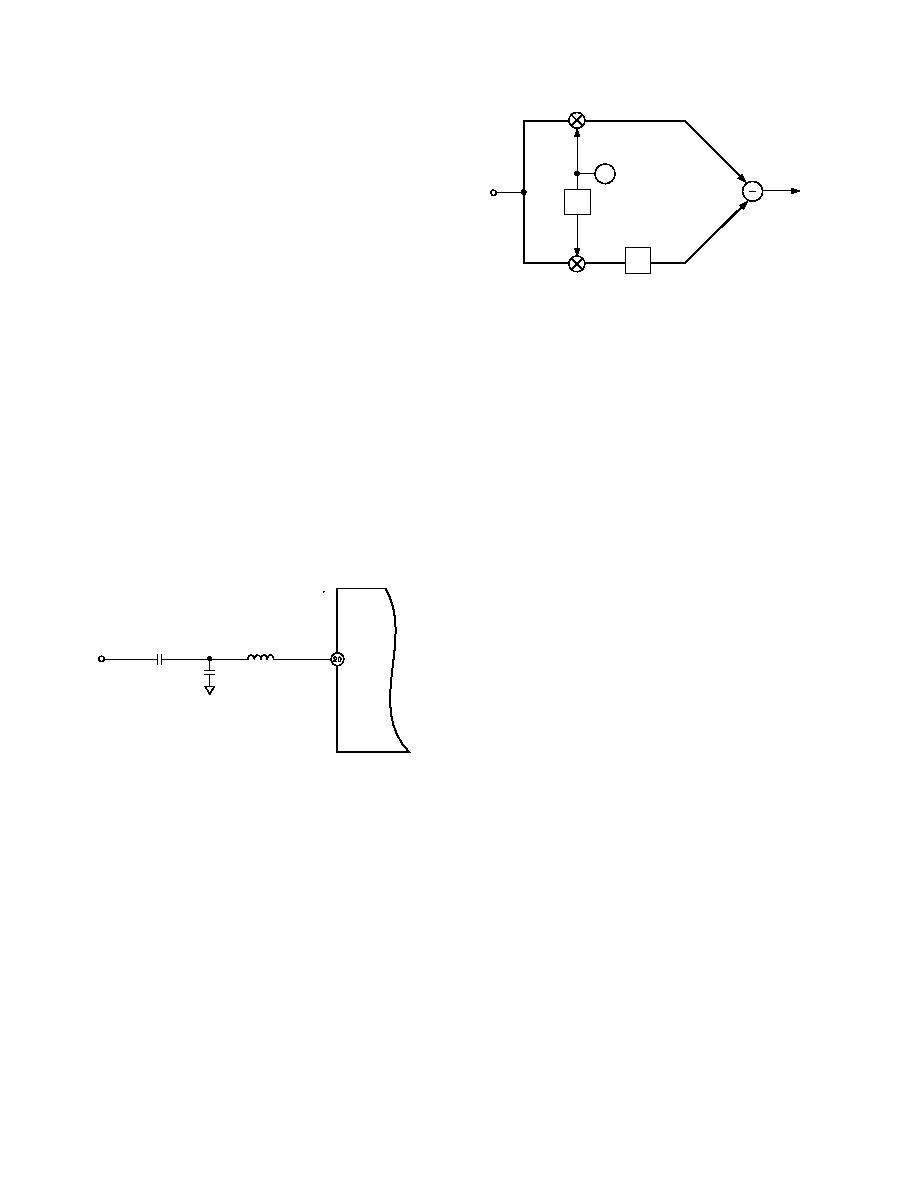
In the AD6190, a technique known as "image-reject" (or SSB)
mixing is used. This technique suppresses image interference by
using a pair of mixers with quadrature local oscillators. See
Figure 9.
90
LO
90
IF
OUT
RF
IN
AD6190
Figure 9. Image-Reject Mixer
The RF signal, containing both the desired signal at (F
LO
+ F
IF
)
and another possible signal at the image frequency of (F
LO
F
IF
) is
applied to two mixers in parallel. These mixers are driven by
local oscillator signals in quadrature. The mixer outputs at the
two mixer IF ports contain both the desired signal and the
image signal. However, the outputs of the two mixers are in
quadrature (shifted 90 degrees relative to each other). The
outputs of the two mixers are then shifted another 90 degrees
relative to each other in a phase-shift network. The two mixer
outputs thus contain the desired signal and the image signal
exactly 180 degrees out of phase. By adding (or subtracting) the
two signals, the undesired image signals cancel, the desired
signal components add, and image-rejection occurs. Local oscil-
lator leakage is suppressed by the use of doubly-balanced mixers.
The quality of the image rejection is a function of the phase and
amplitude matching of the quadrature branches of the LO and
IF phase-shift networks. In the AD6190, image-rejection is
typically 33 dB.
The mixer output that drives the input side of the first
10.7 MHz filter should also be connected through a parallel
RLC network of 6.8 pF, 1 k
, and 7 pF to the power supply to
match the 330
filter impedance.
The 10.7 MHz IF signal is then filtered and amplified by a
24 dB fixed gain. The output of this stage is further filtered, and
applied to a 6-stage limiting amplifier. The limiter output signal
is typically 450 mV p-p into a 30 k
, 30 pF load, with a dc
offset level of approximately 1.76 V dc.
All 10.7 MHz IF filters are assumed to be standard 330
imped-
ance ceramic types. The AD6190 RX IF signal chain and TX IF
input includes internal matching resistors for this impedance.
When used with the Zilog Z87L00 Spread-Spectrum Controller
IC, the 10.7 MHz IF signal contains the received data encoded in
FSK modulation with approximately a
±
33 kHz deviation. The
Z87L00 performs the FSK demodulation in the digital domain.
The RSSI (Received Signal Strength Indicator) signal represents
the strength of the received signal, linear in dB, and scales with
supply voltage. With a 3.3 V supply (through a 10
resistor on
the VCCIF pin), an RF signal level of 100 dBm at the LNA
input will produce an RSSI voltage of approximately 900 mV.
The RSSI voltage will increase with increasing RF input level,
at approximately 22 mV/dB to approximately 2.4 V at
30 dBm input. The RSSI output voltage remains above 2.4 V
for input levels up to +15 dBm.
AD6190
7
REV. 0
Transmit Signal Path
The AD6190 transmit chain is designed to accept an input
signal generated by the Z87L00 device. The Z87L00 provides
a digitally-generated FSK signal at 2.508 MHz, sampled at
8.192 MSPS. This sampling process produces a signal with com-
ponents at 2.508 MHz, 5.684 MHz, 10.7 MHz, 16.386 MHz,
and other higher-order image products at frequencies of (N
×
8.192 MHz
±
2.508) MHz. This signal is filtered to select the
10.7 MHz image, which is used as the transmit IF signal for the
AD6190.
An image-reject transmit up-converts the 10.7 MHz IF signal to
the 902 MHz928 MHz RF band, with image and spurious
outputs typically 45 dB below the desired signal, and LO leak-
age typically 33 dBc.
The on-chip driver can provide at least 1 mW (0 dBm) into a
50
load. However, when driving an external Power Amplifier
(PA) with a gain of 15 dB or more, we recommend a nominal
driver output power no higher than 3 dBm (137 mV p-p TX IF
input level) to avoid spurious PA output products in excess of
FCC allowances. The RFOUT pin is normally connected through
an 8.2 nH dc feed inductor, and ac-coupled to the power amplifier.
TXOUT
2.2pF
8.2nH
TO 50
LOAD
AD6190
+3.3V
Figure 10. TXOUT Matching Circuit
Frequency Control
The AD6190 includes an on-chip voltage controlled oscillator
for LO generation. An external varactor-tuned tank circuit con-
trols the frequency. This VCO operates at twice the required
LO frequency for several reasons.
First, it is a simple matter to generate the I and Q LO compo-
nents needed for the image-reject mixers by starting with a LO
at twice the desired frequency. The divide-by-two process can
easily provide coarse quadrature signals. Any remaining phase
error is further reduced by an on-chip connection network.
Second, by keeping the oscillator operating at a frequency far
removed from the RF carrier frequency, parasitic feedback from
either the transmit signal or strong received signals is minimized.
This reduces VCO "pulling" effects.
A typical series resonant VCO tank circuit is shown in Figure
11. The oscillator actually operates at twice the required LO
frequency band. The tank inductors (L1, L2) may be imple-
mented as printed traces on the PC board or as lumped circuit chip
components. The printed lines are implemented in nonmicrostrip
to produce higher Q. At least two foil layers should be removed
immediately under the tank area. A suitable tank structure can
be formed from two parallel lines, each approximately 7 mm
long by 0.3 mm wide, continuing out from the device pads. In
other words, the Pin 5 and Pin 7 pads are simply extended to
form L1 and L2. Equivalent Hi-Q chip inductors in the 2.2 nH
to 4.7 nH range may be substituted.
The single tuning varactor, D1, (e.g., Alpha Industries SMV-
1233-011) and a fixed capacitor C1 (or a common anode dual
diode) are located on the ends of the lines. Note that this is a
positive supply (VREG) referenced "pump-down" tank, mean-
ing that as the TUNE voltage is increased toward VREG, the
frequency goes down. The loop filter return should also be
referenced to VREG (not ground) in order to minimize com-
mon-mode noise pickup and frequency pushing. The designer is
cautioned to develop a tank with only as much kVCO as re-
quired to allow easy coverage of the band with respect to com-
ponent tolerance and production issues, in order to minimize
phase noise and frequency pulling.
TANK
100nF
C1
15nH
39
AD6190
GND
TANK+
VCLO
82pF
LOOP FILTER
RETURN
(FROM REGULATOR
PASS TRANSISTOR)
15nH
15nH
L2
L1
D1
VTUNE (FROM
LOOP FILTER)
39
Figure 11. Typical VCO Tank Circuit
An on-chip dual-modulus (64/65) prescaler allows the frequency
control to be done with a low-cost low-frequency PLL synthe-
sizer chip, such as the Fujitsu MB87006A, Siemens PMB2307,
or similar.
The prescaler output should be connected to ground through a
2.2 k
pull-down resistor. The output signal (typically 1 V p-p)
is sufficient to drive most low cost PLLs, and is usually ac-
coupled through a 1 nF capacitor to the PLL input.
Layout, Grounding and Decoupling
The AD6190 is a complex device with high bandwidth and high
gain on-chip. Proper layout, grounding and decoupling, tech-
niques are essential to realizing the full performance of the sys-
tem. Each of the power supply pins should be decoupled to
ground at the chip using a 82 pF chip capacitor in parallel with
a 10 nF chip capacitor. The VCCIF pin requires a 10
series
resistor in addition to the 82 pF shunt capacitor.
Voltage Regulator
The AD6190 includes an on-chip voltage regulator to stabilize
the supply voltage for the local oscillator, isolating it from any
variations or noise on the main power supply voltage in the
system. This regulator is nominally set for 2.75 V output. An
external PNP pass transistor provides the needed output current
for the VCO.
This regulator is intended to stabilize the voltage for the LO
only, and should not be used for other circuitry. VBATT may
be connected to a 3.3 V dc preregulator or to the precondi-
tioned three-cell battery system.
AD6190
8
REV. 0
OUTLINE DIMENSIONS
Dimensions shown in inches and (mm).
C323181/98
PRINTED IN U.S.A.
28-Lead Shrink Small Outline
(RS-28)
28
15
14
1
0.407 (10.34)
0.397 (10.08)
0.311 (7.9)
0.301 (7.64)
0.212 (5.38)
0.205 (5.21)
PIN 1
SEATING
PLANE
0.008 (0.203)
0.002 (0.050)
0.07 (1.79)
0.066 (1.67)
0.0256
(0.65)
BSC
0.078 (1.98)
0.068 (1.73)
0.015 (0.38)
0.010 (0.25)
0.009 (0.229)
0.005 (0.127)
0.03 (0.762)
0.022 (0.558)
8
°
0
°
Mode Controls
The AD6190 is designed as a time-division-duplex (TDD)
radio. This means that the transmitter and receiver operate at
different times. The AD6190 includes control pins to shut down
unused portions of the circuit when not needed, saving power,
as shown in the table below. For any mode except "Sleep,"
power must be applied to VBATT Pin 3 and to all VCC Pins
(16, 21 and 26) to ensure proper operation.
NOTE: Do not enable both the transmit and receive paths
simultaneously.
Table I.
Mode
RXON
TXON
VCOON
Notes
Receive
1
0
1
Transmit
0
1
1
"Sleep"
0
0
0
VCO Only
0
0
1
Allows VCO/PLL
to settle prior to
transmit time slot.