 | –≠–ª–µ–∫—Ç—Ä–æ–Ω–Ω—ã–π –∫–æ–º–ø–æ–Ω–µ–Ω—Ç: AD624AD | –°–∫–∞—á–∞—Ç—å:  PDF PDF  ZIP ZIP |

REV. C
Information furnished by Analog Devices is believed to be accurate and
reliable. However, no responsibility is assumed by Analog Devices for its
use, nor for any infringements of patents or other rights of third parties
which may result from its use. No license is granted by implication or
otherwise under any patent or patent rights of Analog Devices.
a
AD624
One Technology Way, P.O. Box 9106, Norwood, MA 02062-9106, U.S.A.
Tel: 781/329-4700
World Wide Web Site: http://www.analog.com
Fax: 781/326-8703
© Analog Devices, Inc., 1999
Precision
Instrumentation Amplifier
PRODUCT DESCRIPTION
The AD624 is a high precision, low noise, instrumentation
amplifier designed primarily for use with low level transducers,
including load cells, strain gauges and pressure transducers. An
outstanding combination of low noise, high gain accuracy, low
gain temperature coefficient and high linearity make the AD624
ideal for use in high resolution data acquisition systems.
The AD624C has an input offset voltage drift of less than
0.25
µ
V/
∞
C, output offset voltage drift of less than 10
µ
V/
∞
C,
CMRR above 80 dB at unity gain (130 dB at G = 500) and a
maximum nonlinearity of 0.001% at G = 1. In addition to these
outstanding dc specifications, the AD624 exhibits superior ac
performance as well. A 25 MHz gain bandwidth product, 5 V/
µ
s
slew rate and 15
µ
s settling time permit the use of the AD624 in
high speed data acquisition applications.
The AD624 does not need any external components for pre-
trimmed gains of 1, 100, 200, 500 and 1000. Additional gains
such as 250 and 333 can be programmed within one percent
accuracy with external jumpers. A single external resistor can
also be used to set the 624's gain to any value in the range of 1
to 10,000.
PRODUCT HIGHLIGHTS
1. The AD624 offers outstanding noise performance. Input
noise is typically less than 4 nV/
Hz at 1 kHz.
2. The AD624 is a functionally complete instrumentation am-
plifier. Pin programmable gains of 1, 100, 200, 500 and 1000
are provided on the chip. Other gains are achieved through
the use of a single external resistor.
3. The offset voltage, offset voltage drift, gain accuracy and gain
temperature coefficients are guaranteed for all pretrimmed
gains.
4. The AD624 provides totally independent input and output
offset nulling terminals for high precision applications.
This minimizes the effect of offset voltage in gain ranging
applications.
5. A sense terminal is provided to enable the user to minimize
the errors induced through long leads. A reference terminal is
also provided to permit level shifting at the output.
FEATURES
Low Noise: 0.2
V p-p 0.1 Hz to 10 Hz
Low Gain TC: 5 ppm max (G = 1)
Low Nonlinearity: 0.001% max (G = 1 to 200)
High CMRR: 130 dB min (G = 500 to 1000)
Low Input Offset Voltage: 25
V, max
Low Input Offset Voltage Drift: 0.25
V/ C max
Gain Bandwidth Product: 25 MHz
Pin Programmable Gains of 1, 100, 200, 500, 1000
No External Components Required
Internally Compensated
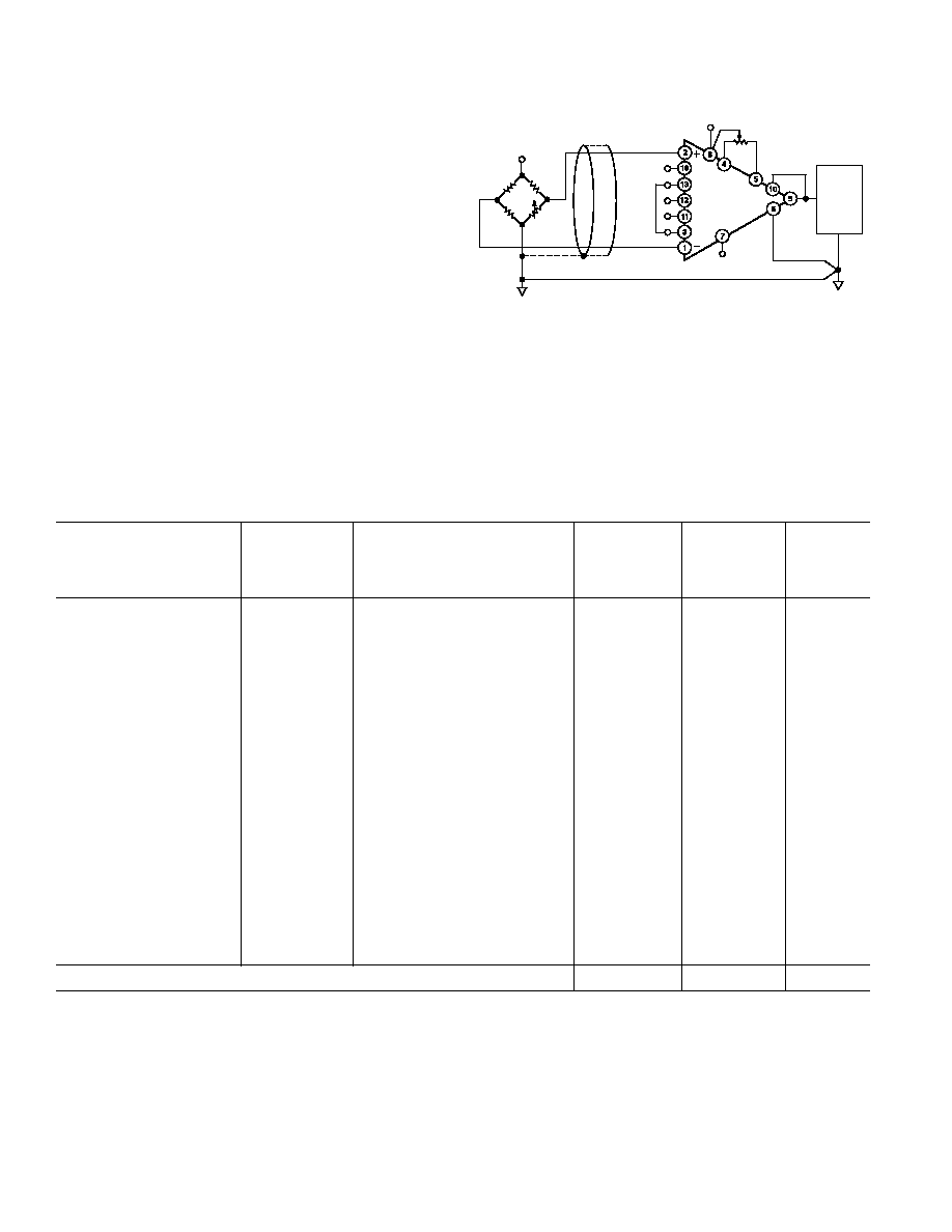
FUNCTIONAL BLOCK DIAGRAM
225.3
124
4445.7
80.2
50
V
B
50
20k
10k
10k
10k
AD624
≠INPUT
G = 100
G = 200
G = 500
RG
1
RG
2
+INPUT
SENSE
OUTPUT
REF
20k
10k

REV. C
≠2≠
AD624≠SPECIFICATIONS
Model
AD624A
AD624B
AD624C
AD624S
Min
Typ
Max
Min
Typ
Max
Min
Typ
Max
Min
Typ
Max
Units
GAIN
Gain Equation
(External Resistor Gain
Programming)
40, 000
R
G
+
1
±
20%
40, 000
R
G
+
1
±
20%
40, 000
R
G
+
1
±
20%
40, 000
R
G
+
1
±
20%
Gain Range (Pin Programmable)
1 to 1000
1 to 1000
1 to 1000
1 to 1000
Gain Error
G = 1
±
0.05
±
0.03
±
0.02
±
0.05
%
G = 100
±
0.25
±
0.15
±
0.1
±
0.25
%
G = 200, 500
±
0.5
±
0.35
±
0.25
±
0.5
%
Nonlinearity
G = 1
±
0.005
±
0.003
±
0.001
±
0.005
%
G = 100, 200
±
0.005
±
0.003
±
0.001
±
0.005
%
G = 500
±
0.005
±
0.005
±
0.005
±
0.005
%
Gain vs. Temperature
G = 1
5
5
5
5
ppm/
∞
C
G = 100, 200
10
10
10
10
ppm/
∞
C
G = 500
25
15
15
15
ppm/
∞
C
VOLTAGE OFFSET (May be Nulled)
Input Offset Voltage
200
75
25
75
µ
V
vs. Temperature
2
0.5
0.25
2.0
µ
V/
∞
C
Output Offset Voltage
5
3
2
3
mV
vs. Temperature
50
25
10
50
µ
V/
∞
C
Offset Referred to the Input vs. Supply
G = 1
70
75
80
75
dB
G = 100, 200
95
105
110
105
dB
G = 500
100
110
115
110
dB
INPUT CURRENT
Input Bias Current
±
50
±
25
±
15
±
50
nA
vs. Temperature
±
50
±
50
±
50
±
50
pA/
∞
C
Input Offset Current
±
35
±
15
±
10
±
35
nA
vs. Temperature
±
20
±
20
±
20
±
20
pA/
∞
C
INPUT
Input Impedance
Differential Resistance
10
9
10
9
10
9
10
9
Differential Capacitance
10
10
10
10
pF
Common-Mode Resistance
10
9
10
9
10
9
10
9
Common-Mode Capacitance
10
10
10
10
pF
Input Voltage Range
1
Max Differ. Input Linear (V
DL
)
±
10
±
10
±
10
±
10
V
Max Common-Mode Linear (V
CM
)
12 V
-
G
2
◊
V
D
12 V
-
G
2
◊
V
D
12 V
-
G
2
◊
V
D
12 V
-
G
2
◊
V
D
V
Common-Mode Rejection dc
to 60 Hz with 1 k
Source Imbalance
G = 1
70
75
80
70
dB
G = 100, 200
100
105
110
100
dB
G = 500
110
120
130
110
dB
OUTPUT RATING
V
OUT
, R
L
= 2 k
±
10
±
10
±
10
±
10
V
DYNAMIC RESPONSE
Small Signal ≠3 dB
G = 1
1
1
1
1
MHz
G = 100
150
150
150
150
kHz
G = 200
100
100
100
100
kHz
G = 500
50
50
50
50
kHz
G = 1000
25
25
25
25
kHz
Slew Rate
5.0
5.0
5.0
5.0
V/
µ
s
Settling Time to 0.01%, 20 V Step
G = 1 to 200
15
15
15
15
µ
s
G = 500
35
35
35
35
µ
s
G = 1000
75
75
75
75
µ
s
NOISE
Voltage Noise, 1 kHz
R.T.I.
4
4
4
4
nV/
Hz
R.T.O.
75
75
75
75
nV/
Hz
R.T.I., 0.1 Hz to 10 Hz
G = 1
10
10
10
10
µ
V p-p
G = 100
0.3
0.3
0.3
0.3
µ
V p-p
G = 200, 500, 1000
0.2
0.2
0.2
0.2
µ
V p-p
Current Noise
0.1 Hz to 10 Hz
60
60
60
60
pA p-p
SENSE INPUT
R
IN
8
10
12
8
10
12
8
10
12
8
10
12
k
I
IN
30
30
30
30
µ
A
Voltage Range
±
10
±
10
±
10
±
10
V
Gain to Output
1
1
1
1
%
(@ V
S
= 15 V, R
L
= 2 k and T
A
= +25 C, unless otherwise noted)
REV. C
≠3≠
AD624
Model
AD624A
AD624B
AD624C
AD624S
Min
Typ
Max
Min
Typ
Max
Min
Typ
Max
Min
Typ
Max
Units
REFERENCE INPUT
R
IN
16
20
24
16
20
24
16
20
24
16
20
24
k
I
IN
30
30
30
30
µ
A
Voltage Range
±
10
±
10
±
10
±
10
V
Gain to Output
1
1
1
1
%
TEMPERATURE RANGE
Specified Performance
≠25
+85
≠25
+85
≠25
+85
≠55
+125
∞
C
Storage
≠65
+150
≠65
+150
≠65
+150
≠65
+150
∞
C
POWER SUPPLY
Power Supply Range
6
15
18
6
15
18
6
15
18
6
15
18
V
Quiescent Current
3.5
5
3.5
5
3.5
5
3.5
5
mA
NOTES
1
V
DL
is the maximum differential input voltage at G = 1 for specified nonlinearity, V
DL
at other gains = 10 V/G. V
D
= actual differential input voltage.
1
Example: G = 10, V
D
= 0.50. V
CM
= 12 V ≠ (10/2
◊
0.50 V) = 9.5 V.
Specifications subject to change without notice.
Specifications shown in boldface are tested on all production unit at final electrical test. Results from those tests are used to calculate outgoing quality levels. All min
and max specifications are guaranteed, although only those shown in boldface are tested on all production units.
ABSOLUTE MAXIMUM RATINGS*
Supply Voltage . . . . . . . . . . . . . . . . . . . . . . . . . . . . . . . .
±
18 V
Internal Power Dissipation . . . . . . . . . . . . . . . . . . . . . 420 mW
Input Voltage . . . . . . . . . . . . . . . . . . . . . . . . . . . . . . . . . . .
±
V
S
Differential Input Voltage . . . . . . . . . . . . . . . . . . . . . . . . .
±
V
S
Output Short Circuit Duration . . . . . . . . . . . . . . . . Indefinite
Storage Temperature Range . . . . . . . . . . . . . ≠65
∞
C to +150
∞
C
Operating Temperature Range
AD624A/B/C . . . . . . . . . . . . . . . . . . . . . . . ≠25
∞
C to +85
∞
C
AD624S . . . . . . . . . . . . . . . . . . . . . . . . . . . ≠55
∞
C to +125
∞
C
Lead Temperature (Soldering, 60 secs) . . . . . . . . . . . . +300
∞
C
*Stresses above those listed under Absolute Maximum Ratings may cause perma-
nent damage to the device. This is a stress rating only; functional operation of the
device at these or any other conditions above those indicated in the operational
sections of this specification is not implied. Exposure to absolute maximum rating
conditions for extended periods may affect device reliability.
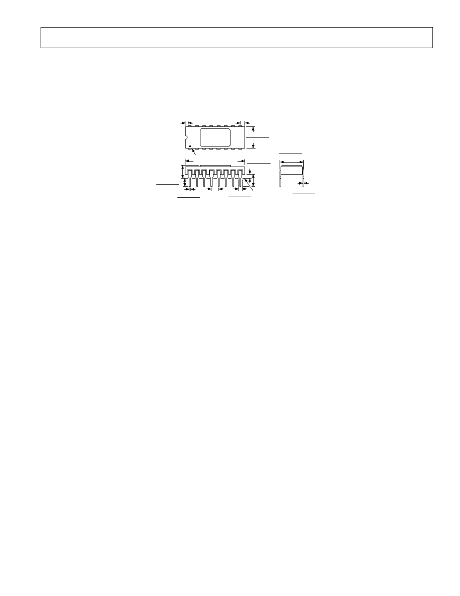
CONNECTION DIAGRAM
≠INPUT
+INPUT
RG
1
OUTPUT NULL
INPUT NULL
REF
≠V
S
G = 200
G = 500
SENSE
RG
2
INPUT NULL
OUTPUT NULL
G = 100
+V
S
OUTPUT
1
2
5
6
7
3
4
8
16
15
12
11
10
14
13
9
TOP VIEW
(Not to Scale)
AD624
SHORT TO
RG
2
FOR
DESIRED
GAIN
FOR GAINS OF 1000 SHORT RG
1
TO PIN 12
AND PINS 11 AND 13 TO RG
2
METALIZATION PHOTOGRAPH
Contact factory for latest dimensions
Dimensions shown in inches and (mm).
ORDERING GUIDE
Temperature
Package
Package
Model
Range
Description
Option
AD624AD
≠25
∞
C to +85
∞
C
16-Lead Ceramic DIP D-16
AD624BD
≠25
∞
C to +85
∞
C
16-Lead Ceramic DIP D-16
AD624CD
≠25
∞
C to +85
∞
C
16-Lead Ceramic DIP D-16
AD624SD
≠55
∞
C to +125
∞
C 16-Lead Ceramic DIP D-16
AD624SD/883B* ≠55
∞
C to +125
∞
C 16-Lead Ceramic DIP D-16
AD624AChips
≠25
∞
C to +85
∞
C
Die
AD624SChips
≠25
∞
C to +85
∞
C
Die
*See Analog Devices' military data sheet for 883B specifications.
REV. C
AD624≠Typical Characteristics
20
0
0
20
15
5
5
10
15
10
SUPPLY VOLTAGE ≠ V
INPUT VOLTAGE RANGE ≠
V
+25 C
Figure 1. Input Voltage Range vs.
Supply Voltage, G = 1
8.0
0
0
20
6.0
2.0
5
4.0
15
10
SUPPLY VOLTAGE ≠ V
AMPLIFIER QUIESCENT CURRENT ≠ mA
Figure 4. Quiescent Current vs.
Supply Voltage
16
0
20
4
2
5
0
8
6
10
12
14
15
10
INPUT VOLTAGE ≠ V
INPUT BIAS CURRENT ≠
nA
Figure 7. Input Bias Current vs. CMV
20
0
0
20
15
5
5
10
15
10
SUPPLY VOLTAGE ≠ V
OUTPUT VOLTAGE SWING ≠
V
Figure 2. Output Voltage Swing vs.
Supply Voltage
16
0
20
4
2
5
0
8
6
10
12
14
15
10
SUPPLY VOLTAGE ≠ V
INPUT BIAS CURRENT ≠
nA
Figure 5. Input Bias Current vs.
Supply Voltage
≠1
7
8.0
5
6
1.0
0
3
4
2
1
0
7.0
6.0
5.0
4.0
3.0
2.0
WARM-UP TIME ≠ Minutes
VOS FROM FINAL VALUE ≠
V
Figure 8. Offset Voltage, RTI, Turn
On Drift
10
100
10k
1k
30
20
0
10
LOAD RESISTANCE ≠
OUTPUT VOLTAGE SWING ≠ V p-p
Figure 3. Output Voltage Swing vs.
Load Resistance
40
≠40
125
≠20
≠30
≠75
0
≠10
10
20
30
75
25
≠25
TEMPERATURE ≠ C
INPUT BIAS CURRENT ≠ nA
≠125
Figure 6. Input Bias Current vs.
Temperature
0
500
100
10
1
1
10
10M
1M
100k
10k
1k
100
FREQUENCY ≠ Hz
GAIN ≠ V/V
Figure 9. Gain vs. Frequency
≠4≠

REV. C
AD624
≠5≠
0
1
10
10M
1M
100k
10k
1k
100
FREQUENCY ≠ Hz
≠100
≠80
≠60
≠40
CMRR ≠ dB
≠120
≠140
≠20
G = 500
G = 1
G = 100
Figure 10. CMRR vs. Frequency RTI,
Zero to 1k Source Imbalance
160
0
100k
40
20
10
80
60
100
120
140
10k
1k
100
FREQUENCY ≠ Hz
POWER SUPPLY REJECTION ≠ dB
G = 500
G = 100
G = 1
≠V
S
= ≠15V dc+
1V p-p SINEWAVE
Figure 13. Negative PSRR vs.
Frequency
Figure 16. Low Frequency Voltage
Noise
,
G = 1 (System Gain = 1000)
30
20
0
10
FULL-POWER RESPONSE ≠ V p-p
FREQUENCY ≠ Hz
10k
1k
100k
1M
G = 1, 100
G = 500
G = 100
G = 1000
BANDWIDTH LIMITED
-
Figure 11. Large Signal Frequency
Response
VOLT NSD ≠ nV/
Hz
0.1
100
1
10
1000
100k
10
1
10k
1k
100
FREQUENCY ≠ Hz
G = 1
G = 10
G = 100, 1000
G = 1000
Figure 14. RTI Noise Spectral
Density vs. Gain
Figure 17. Low Frequency Voltage
Noise, G = 1000 (System Gain =
100,000)
160
0
100k
40
20
10
80
60
100
120
140
10k
1k
100
FREQUENCY ≠ Hz
POWER SUPPLY REJECTION ≠ dB
G = 500
G = 100
G = 1
≠V
S
= ≠15V dc+
1V p-p SINEWAVE
Figure 12. Positive PSRR vs.
Frequency
10
10k
100
1000
100k
100k
1
0.1
10k
100
10
FREQUENCY ≠ Hz
CURRENT NOISE SPECTRAL DENSITY ≠ fA/
Hz
Figure 15. Input Current Noise
20
8 TO ≠8
12 TO ≠12
0
OUTPUT
STEP ≠V
4 TO ≠4
≠4 TO 4
≠8 TO 8
≠12 TO 12
15
10
5
SETTLING TIME ≠ s
1%
1%
0.1%
0.01%
0.1%
0.01%
Figure 18. Settling Time, Gain = 1
REV. C
AD624
≠6≠
Figure 19. Large Signal Pulse
Response and Settling Time, G = 1
Figure 22. Range Signal Pulse
Response and Settling Time,
G = 500
20
8 TO ≠8
12 TO ≠12
0
OUTPUT
STEP ≠V
4 TO ≠4
≠4 TO 4
≠8 TO 8
≠12 TO 12
15
10
5
SETTLING TIME ≠ s
1%
1%
0.1%
0.01%
0.1%
0.01%
Figure 20. Settling Time Gain = 100
20
8 TO ≠8
12 TO ≠12
0
OUTPUT
STEP ≠V
4 TO ≠4
≠4 TO 4
≠8 TO 8
≠12 TO 12
15
10
5
SETTLING TIME ≠ s
0.1%
0.1%
1%
1%
0.01%
0.01%
Figure 23. Settling Time Gain = 1000
Figure 21. Large Signal Pulse
Response and Settling Time,
G = 100
Figure 24. Large Signal Pulse
Response and Settling Time,
G = 1000
REV. C
AD624
≠7≠
AD624
+V
S
V
OUT
10k
1%
1k
10T
10k
1%
RG
1
G = 100
G = 200
G = 500
RG
2
≠V
S
200
0.1%
100k
1%
500
0.1%
1k
0.1%
INPUT
20V p-p
Figure 25. Settling Time Test Circuit
THEORY OF OPERATION
The AD624 is a monolithic instrumentation amplifier based on
a modification of the classic three-op-amp instrumentation
amplifier. Monolithic construction and laser-wafer-trimming
allow the tight matching and tracking of circuit components and
the high level of performance that this circuit architecture is ca-
pable of.
A preamp section (Q1≠Q4) develops the programmed gain by
the use of feedback concepts. Feedback from the outputs of A1
and A2 forces the collector currents of Q1≠Q4 to be constant
thereby impressing the input voltage across R
G
.
The gain is set by choosing the value of R
G
from the equation,
Gain =
40
k
R
G
+ 1. The value of R
G
also sets the transconduct-
ance of the input preamp stage increasing it asymptotically to
the transconductance of the input transistors as R
G
is reduced
for larger gains. This has three important advantages. First, this
approach allows the circuit to achieve a very high open loop gain
of 3
◊
10
8
at a programmed gain of 1000 thus reducing gain
related errors to a negligible 3 ppm. Second, the gain bandwidth
product which is determined by C3 or C4 and the input trans-
conductance, reaches 25 MHz. Third, the input voltage noise
reduces to a value determined by the collector current of the
input transistors for an RTI noise of 4 nV/
Hz at G
500.
AD624
+V
S
100
200
RG
2
≠V
S
16.2k
+V
S
1/2
AD712
9.09k
G1, 100, 200
1k
1 F
G500
100
1 F
1.62M
≠V
S
1 F
16.2k
1.82k
500
1/2
AD712
Figure 26. Noise Test Circuit
INPUT CONSIDERATIONS
Under input overload conditions the user will see R
G
+ 100
and two diode drops (~1.2 V) between the plus and minus
inputs, in either direction. If safe overload current under all
conditions is assumed to be 10 mA, the maximum overload
voltage is ~
±
2.5 V. While the AD624 can withstand this con-
tinuously, momentary overloads of
±
10 V will not harm the
device. On the other hand the inputs should never exceed the
supply voltage.
The AD524 should be considered in applications that require
protection from severe input overload. If this is not possible,
external protection resistors can be put in series with the inputs
of the AD624 to augment the internal (50
) protection resis-
tors. This will most seriously degrade the noise performance.
For this reason the value of these resistors should be chosen to
be as low as possible and still provide 10 mA of current limiting
under maximum continuous overload conditions. In selecting
the value of these resistors, the internal gain setting resistor and
the 1.2 volt drop need to be considered. For example, to pro-
tect the device from a continuous differential overload of 20 V
at a gain of 100, 1.9 k
of resistance is required. The internal
gain resistor is 404
; the internal protect resistor is 100
.
There is a 1.2 V drop across D1 or D2 and the base-emitter
junction of either Q1 and Q3 or Q2 and Q4 as shown in Figure
27, 1400
of external resistance would be required (700
in
series with each input). The RTI noise in this case would be
4
KTR
ext
+
(4
nV / Hz )
2
=
6.2
nV / Hz
50
13
50 A
I1
50 A
C3
I2
50 A
R57
20k
R56
20k
500
SENSE
+IN
V
O
REF
I4
50 A
200
100
4445
80.2
124
225.3
≠IN
≠V
S
RG
1
RG
2
C4
VB
A2
R52
10k
R55
10k
A3
R53
10k
R54
10k
+V
S
50
Q1, Q3
Q2,
Q4
A1
Figure 27. Simplified Circuit of Amplifier; Gain Is Defined
as (R56 + R57)/(R
G
) + 1. For a Gain of 1, R
G
Is an Open
Circuit.
INPUT OFFSET AND OUTPUT OFFSET
Voltage offset specifications are often considered a figure of
merit for instrumentation amplifiers. While initial offset may
be adjusted to zero, shifts in offset voltage due to temperature
variations will cause errors. Intelligent systems can often correct
for this factor with an autozero cycle, but there are many small-
signal high-gain applications that don't have this capability.
Voltage offset and offset drift each have two components; input
and output. Input offset is that component of offset that is

REV. C
AD624
≠8≠
directly proportional to gain i.e., input offset as measured at
the output at G = 100 is 100 times greater than at G = 1.
Output offset is independent of gain. At low gains, output offset
drift is dominant, while at high gains input offset drift domi-
nates. Therefore, the output offset voltage drift is normally
specified as drift at G = 1 (where input effects are insignificant),
while input offset voltage drift is given by drift specification at a
high gain (where output offset effects are negligible). All input-
related numbers are referred to the input (RTI) which is to say
that the effect on the output is "G" times larger. Voltage offset
vs. power supply is also specified at one or more gain settings
and is also RTI.
By separating these errors, one can evaluate the total error inde-
pendent of the gain setting used. In a given gain configura-
tion both errors can be combined to give a total error referred to
the input (R.T.I.) or output (R.T.O.) by the following formula:
Total Error R.T.I. = input error + (output error/gain)
Total Error R.T.O. = (Gain
◊
input error) + output error
As an illustration, a typical AD624 might have a +250
µ
V out-
put offset and a ≠50
µ
V input offset. In a unity gain configura-
tion, the
total output offset would be 200
µ
V or the sum of the
two. At a gain of 100, the output offset would be ≠4.75 mV
or: +250
µ
V + 100 (≠50
µ
V) = ≠4.75 mV.
The AD624 provides for both input and output offset adjust-
ment. This optimizes nulling in very high precision applications
and minimizes offset voltage effects in switched gain applica-
tions. In such applications the input offset is adjusted first at the
highest programmed gain, then the output offset is adjusted at
G = 1.
GAIN
The AD624 includes high accuracy pretrimmed internal
gain resistors. These allow for single connection program-
ming of gains of 1, 100, 200 and 500. Additionally, a variety
of gains including a pretrimmed gain of 1000 can be achieved
through series and parallel combinations of the internal resis-
tors. Table I shows the available gains and the appropriate
pin connections and gain temperature coefficients.
The gain values achieved via the combination of internal
resistors are extremely useful. The temperature coefficient of the
gain is dependent primarily on the mismatch of the temperature
coefficients of the various internal resistors. Tracking of these
resistors is extremely tight resulting in the low gain TCs shown
in Table I.
If the desired value of gain is not attainable using the inter-
nal resistors, a single external resistor can be used to achieve
any gain between 1 and 10,000. This resistor connected between
AD624
G = 100
RG
2
≠V
S
OUTPUT
SIGNAL
COMMON
V
OUT
10k
≠INPUT
RG
1
G = 200
G = 500
+INPUT
INPUT
OFFSET
NULL
+V
S
Figure 28. Operating Connections for G = 200
Table I.
Temperature
Gain
Coefficient
Pin 3
(Nominal)
(Nominal)
to Pin
Connect Pins
1
≠0 ppm/
∞
C
≠
≠
100
≠1.5 ppm/
∞
C
13
≠
125
≠5 ppm/
∞
C
13
11 to 16
137
≠5.5 ppm/
∞
C
13
11 to 12
186.5
≠6.5 ppm/
∞
C
13
11 to 12 to 16
200
≠3.5 ppm/
∞
C
12
≠
250
≠5.5 ppm/
∞
C
12
11 to 13
333
≠15 ppm/
∞
C
12
11 to 16
375
≠0.5 ppm/
∞
C
12
13 to 16
500
≠10 ppm/
∞
C
11
≠
624
≠5 ppm/
∞
C
11
13 to 16
688
≠1.5 ppm/
∞
C
11
11 to 12; 13 to 16
831
+4 ppm/
∞
C
11
16 to 12
1000
0 ppm/
∞
C
11
16 to 12; 13 to 11
Pins 3 and 16 programs the gain according to the formula
R
G
=
40
k
G
-
1
(see Figure 29). For best results R
G
should be a precision resis-
tor with a low temperature coefficient. An external R
G
affects both
gain accuracy and gain drift due to the mismatch between it and
the internal thin-film resistors R56 and R57. Gain accuracy is
determined by the tolerance of the external R
G
and the absolute
accuracy of the internal resistors (
±
20%). Gain drift is determined
by the mismatch of the temperature coefficient of R
G
and the tem-
perature coefficient of the internal resistors (≠15 ppm/
∞
C typ),
and the temperature coefficient of the internal interconnections.
AD624
RG
2
≠V
S
REFERENCE
V
OUT
≠INPUT
RG
1
2.105k
+INPUT
+V
S
OR
1.5k
1k
G = + 1 = 20 20%
40.000
2.105
Figure 29. Operating Connections for G = 20
The AD624 may also be configured to provide gain in the out-
put stage. Figure 30 shows an H pad attenuator connected to
the reference and sense lines of the AD624. The values of R1,
R2 and R3 should be selected to be as low as possible to mini-
mize the gain variation and reduction of CMRR. Varying R2
will precisely set the gain without affecting CMRR. CMRR is
determined by the match of R1 and R3.
AD624
G = 100
RG
2
≠V
S
V
OUT
≠INPUT
RG
1
G = 200
G = 500
+INPUT
+V
S
R
L
R3
6k
R2
5k
R1
6k
(R
2
||20k ) + R
1
+ R
3
)
(R
2
||20k )
G =
(R
1
+ R
2
+ R
3
) || R
L
2k
Figure 30. Gain of 2500
REV. C
AD624
≠9≠
NOISE
The AD624 is designed to provide noise performance near the
theoretical noise floor. This is an extremely important design
criteria as the front end noise of an instrumentation amplifier is
the ultimate limitation on the resolution of the data acquisition
system it is being used in. There are two sources of noise in an
instrument amplifier, the input noise, predominantly generated
by the differential input stage, and the output noise, generated
by the output amplifier. Both of these components are present
at the input (and output) of the instrumentation amplifier. At
the input, the input noise will appear unaltered; the output
noise will be attenuated by the closed loop gain (at the output,
the output noise will be unaltered; the input noise will be ampli-
fied by the closed loop gain). Those two noise sources must be
root sum squared to determine the total noise level expected at
the input (or output).
The low frequency (0.1 Hz to 10 Hz) voltage noise due to the
output stage is 10
µ
V p-p, the contribution of the input stage is
0.2
µ
V p-p. At a gain of 10, the RTI voltage noise would be
1
µ
V p-p,
10
G
2
+
0.2
( )
2
. The RTO voltage noise would be
10.2
µ
V p-p,
10
2
+
0.2
G
( )
(
)
2
. These calculations hold for
applications using either internal or external gain resistors.
INPUT BIAS CURRENTS
Input bias currents are those currents necessary to bias the input
transistors of a dc amplifier. Bias currents are an additional
source of input error and must be considered in a total error
budget. The bias currents when multiplied by the source resis-
tance imbalance appear as an additional offset voltage. (What is
of concern in calculating bias current errors is the change in bias
current with respect to signal voltage and temperature.) Input
offset current is the difference between the two input bias cur-
rents. The effect of offset current is an input offset voltage whose
magnitude is the offset current times the source resistance.
AD624
≠V
S
+V
S
LOAD
TO
POWER
SUPPLY
GROUND
a. Transformer Coupled
AD624
≠V
S
+V
S
LOAD
TO
POWER
SUPPLY
GROUND
b. Thermocouple
AD624
≠V
S
+V
S
LOAD
TO
POWER
SUPPLY
GROUND
c. AC-Coupled
Figure 31. Indirect Ground Returns for Bias Currents
Although instrumentation amplifiers have differential inputs,
there must be a return path for the bias currents. If this is not
provided, those currents will charge stray capacitances, causing
the output to drift uncontrollably or to saturate. Therefore,
when amplifying "floating" input sources such as transformers
and thermocouples, as well as ac-coupled sources, there must
still be a dc path from each input to ground, (see Figure 31).
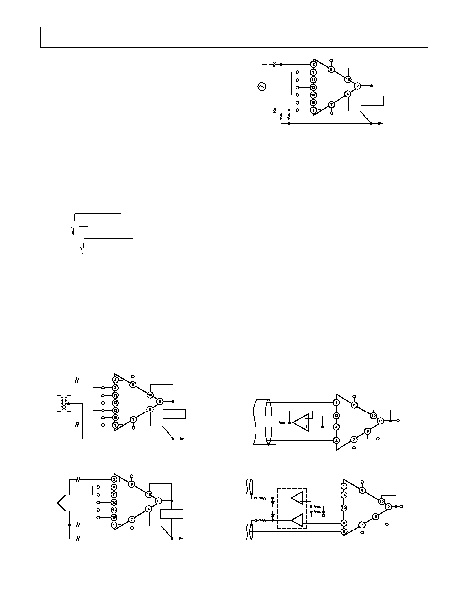
COMMON-MODE REJECTION
Common-mode rejection is a measure of the change in output
voltage when both inputs are changed by equal amounts. These
specifications are usually given for a full-range input voltage
change and a specified source imbalance. "Common-Mode
Rejection Ratio" (CMRR) is a ratio expression while "Common-
Mode Rejection" (CMR) is the logarithm of that ratio. For
example, a CMRR of 10,000 corresponds to a CMR of 80 dB.
In an instrumentation amplifier, ac common-mode rejection is
only as good as the differential phase shift. Degradation of ac
common-mode rejection is caused by unequal drops across
differing track resistances and a differential phase shift due to
varied stray capacitances or cable capacitances. In many appli-
cations shielded cables are used to minimize noise. This tech-
nique can create common-mode rejection errors unless the
shield is properly driven. Figures 32 and 33 shows active data
guards which are configured to improve ac common-mode
rejection by "bootstrapping" the capacitances of the input
cabling, thus minimizing differential phase shift.
AD624
RG
2
≠V
S
REFERENCE
V
OUT
≠INPUT
+INPUT
+V
S
G = 200
AD711
100
Figure 32. Shield Driver, G
100
AD624
RG
1
≠V
S
REFERENCE
V
OUT
≠INPUT
+INPUT
+V
S
≠V
S
AD712
100
100
RG
2
Figure 33. Differential Shield Driver
REV. C
AD624
≠10≠
GROUNDING
Many data-acquisition components have two or more ground
pins which are not connected together within the device. These
grounds must be tied together at one point, usually at the sys-
tem power supply ground. Ideally, a single solid ground would
be desirable. However, since current flows through the ground
wires and etch stripes of the circuit cards, and since these paths
have resistance and inductance, hundreds of millivolts can be
generated between the system ground point and the data acqui-
sition components. Separate ground returns should be provided
to minimize the current flow in the path from the most sensitive
points to the system ground point. In this way supply currents
and logic-gate return currents are not summed into the same
return path as analog signals where they would cause measure-
ment errors (see Figure 34).
OUTPUT
REFERENCE
ANALOG
GROUND*
*IF INDEPENDENT, OTHERWISE RETURN AMPLIFIER REFERENCE
TO MECCA AT ANALOG P.S. COMMON
SIGNAL
GROUND
AD574A
DIGITAL
DATA
OUTPUT
+
1 F
0.1
F
1 F
1 F
DIG
COM
0.1
F
0.1
F
0.1
F
AD624
SAMPLE
AND HOLD
AD583
ANALOG P.S.
+15V C ≠15V
+5V
DIGITAL P.S.
C
Figure 34. Basic Grounding Practice
Since the output voltage is developed with respect to the poten-
tial on the reference terminal an instrumentation amplifier can
solve many grounding problems.
SENSE TERMINAL
The sense terminal is the feedback point for the instrument
amplifier's output amplifier. Normally it is connected to the
instrument amplifier output. If heavy load currents are to be
drawn through long leads, voltage drops due to current flowing
through lead resistance can cause errors. The sense terminal can
be wired to the instrument amplifier at the load thus putting the
IxR drops "inside the loop" and virtually eliminating this error
source.
AD624
V+
OUTPUT
CURRENT
BOOSTER
V≠
V
IN
+
V
IN
≠
X1
R
L
(REF)
(SENSE)
Figure 35. AD624 Instrumentation Amplifier with Output
Current Booster
Typically, IC instrumentation amplifiers are rated for a full
±
10 volt output swing into 2 k
. In some applications, how-
ever, the need exists to drive more current into heavier loads.
Figure 35 shows how a current booster may be connected
"inside the loop" of an instrumentation amplifier to provide the
required current without significantly degrading overall perfor-
mance. The effects of nonlinearities, offset and gain inaccuracies
of the buffer are reduced by the loop gain of the IA output
amplifier. Offset drift of the buffer is similarly reduced.
REFERENCE TERMINAL
The reference terminal may be used to offset the output by up
to
±
10 V. This is useful when the load is "floating" or does not
share a ground with the rest of the system. It also provides a
direct means of injecting a precise offset. It must be remem-
bered that the total output swing is
±
10 volts, from ground, to
be shared between signal and reference offset.
AD624
V
IN
+
V
IN
≠
REF
SENSE
LOAD
AD711
≠V
S
+V
S
V
OFFSET
Figure 36. Use of Reference Terminal to Provide Output
Offset
When the IA is of the three-amplifier configuration it is neces-
sary that nearly zero impedance be presented to the reference
terminal. Any significant resistance, including those caused by
PC layouts or other connection techniques, which appears
between the reference pin and ground will increase the gain of
the noninverting signal path, thereby upsetting the common-
mode rejection of the IA. Inadvertent thermocouple connections
created in the sense and reference lines should also be avoided
as they will directly affect the output offset voltage and output
offset voltage drift.
In the AD624 a reference source resistance will unbalance the
CMR trim by the ratio of 10 k
/R
REF
. For example, if the refer-
ence source impedance is 1
, CMR will be reduced to 80 dB
(10 k
/1
= 80 dB). An operational amplifier may be used to
provide that low impedance reference point as shown in Figure
36. The input offset voltage characteristics of that amplifier will
add directly to the output offset voltage performance of the
instrumentation amplifier.
An instrumentation amplifier can be turned into a voltage-to-
current converter by taking advantage of the sense and reference
terminals as shown in Figure 37.
AD624
+INPUT
REF
R
1
+V
X
≠
SENSE
LOAD
AD711
A2
I
L
≠INPUT
40.000
R
G
1 +
I
L
= =
V
X
R
1
V
IN
R
1
Figure 37. Voltage-to-Current Converter
REV. C
AD624
≠11≠
By establishing a reference at the "low" side of a current setting
resistor, an output current may be defined as a function of input
voltage, gain and the value of that resistor. Since only a small
current is demanded at the input of the buffer amplifier A2, the
forced current I
L
will largely flow through the load. Offset and
drift specifications of A2 must be added to the output offset and
drift specifications of the IA.
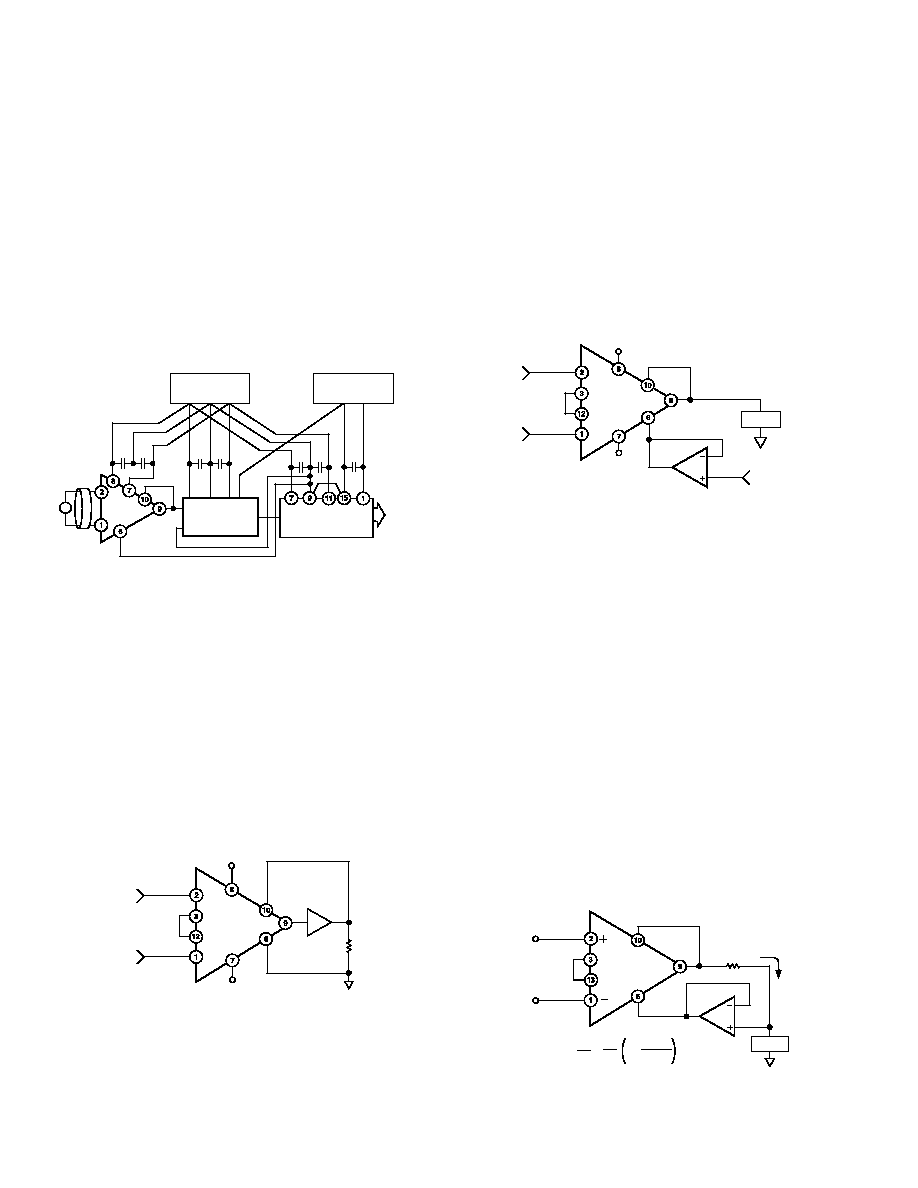
PROGRAMMABLE GAIN
Figure 38 shows the AD624 being used as a software program-
mable gain amplifier. Gain switching can be accomplished with
mechanical switches such as DIP switches or reed relays. It
should be noted that the "on" resistance of the switch in series
with the internal gain resistor becomes part of the gain equation
and will have an effect on gain accuracy.
A significant advantage in using the internal gain resistors in a
programmable gain configuration is the minimization of thermo-
couple signals which are often present in multiplexed data
acquisition systems.
If the full performance of the AD624 is to be achieved, the user
must be extremely careful in designing and laying out his circuit
to minimize the remaining thermocouple signals.
The AD624 can also be connected for gain in the output stage.
Figure 39 shows an AD547 used as an active attenuator in the
output amplifier's feedback loop. The active attenuation pre-
sents a very low impedance to the feedback resistors therefore
minimizing the common-mode rejection ratio degradation.
Another method for developing the switching scheme is to use a
DAC. The AD7528 dual DAC which acts essentially as a pair of
switched resistive attenuators having high analog linearity and
symmetrical bipolar transmission is ideal in this application. The
multiplying DAC's advantage is that it can handle inputs of
either polarity or zero without affecting the programmed gain.
The circuit shown uses an AD7528 to set the gain (DAC A) and
to perform a fine adjustment (DAC B).
V
DD
GND
225.3
124
4445.7
80.2
50
16
15
14
13
12
11
10
9
1
2
3
4
5
6
7
8
10k
20k
V
B
20k
10k
10k
50
≠V
S
+V
S
1 F
35V
≠IN
+IN
10k
10k
INPUT
OFFSET
NULL
OUTPUT
OFFSET
NULL
10k
TO ≠V
(+INPUT)
(≠INPUT)
V
OUT
39.2k
WR
A4
A3
A2
A1
V
SS
1k
10pF
+V
S
28.7k
316k
1k
1k
≠V
S
AD624
AD7590
AD711
Figure 39. Programmable Output Gain
225.3
124
4445.7
80.2
50
G = 100
K1
16
15
14
13
12
11
10
9
1
2
3
4
5
6
7
8
10k
20k
V
B
20k
10k
10k
50
≠V
S
+V
S
1 F
35V
≠IN
+IN
R2
10k
R1
10k
INPUT
OFFSET
TRIM
OUTPUT
OFFSET
TRIM
RELAY
SHIELDS
G = 200
K2
G = 500
K3
D1
D2
D3
Y0
K2
K3
74LS138
DECODER
7407N
BUFFER
DRIVER
A
B
Y1
Y2
INPUTS
GAIN
RANGE
+5V
10 F
C1
C2
K1 ≠ K3 =
THERMOSEN DM2C
4.5V COIL
D1 ≠ D3 = IN4148
ANALOG
COMMON
GAIN TABLE
A
B
GAIN
0
0
100
0
1
500
1
0
200
1
1
1
LOGIC
COMMON
K1
OUT
10k
+5V
AD624
NC
Figure 38. Gain Programmable Amplifier

REV. C
AD624
≠12≠
225.3
124
4445.7
80.2
50
V
B
50
20k
10k
10k
10k
AD624
G = 100
G = 200
G = 500
RG
1
RG
2
≠INPUT
(+INPUT)
V
OUT
20k
10k
+INPUT
(≠INPUT)
AD7528
1/2
AD712
256:1
DATA
INPUTS
CS
WR
DAC A
/DAC B
DB0
DB7
+V
S
DAC A
DAC B
1/2
AD712
Figure 40. Programmable Output Gain Using a DAC
AUTOZERO CIRCUITS
In many applications it is necessary to provide very accurate
data in high gain configurations. At room temperature the offset
effects can be nulled by the use of offset trimpots. Over the
operating temperature range, however, offset nulling becomes a
problem. The circuit of Figure 41 shows a CMOS DAC operat-
ing in the bipolar mode and connected to the reference terminal
to provide software controllable offset adjustments.
AD624
≠V
S
+V
S
V
OUT
G = 100
G = 200
G = 500
RG
1
RG
2
+INPUT
≠INPUT
DATA
INPUTS
CS
WR
MSB
LSB
+V
S
AD7524
C1
OUT1
OUT2
1/2
AD712
R
FB
+V
S
R3
20k
R4
10k
R5
20k
≠V
S
R6
5k
≠V
S
GND
AD589
39k
V
REF
1/2
AD712
Figure 41. Software Controllable Offset
In many applications complex software algorithms for autozero
applications are not available. For these applications Figure 42
provides a hardware solution.
AD624
≠V
S
+V
S
V
OUT
RG
1
RG
2
1k
12 11
9 10
0.1 F LOW
LEAKAGE
CH
15
16
14
13
V
SS
V
DD
GND
A1
A2
A3
A4
AD7510DIKD
200 s
ZERO PULSE
AD542
Figure 42. Autozero Circuit
The microprocessor controlled data acquisition system shown in
Figure 43 includes includes both autozero and autogain capabil-
ity. By dedicating two of the differential inputs, one to ground
and one to the A/D reference, the proper program calibration
cycles can eliminate both initial accuracy errors and accuracy
errors over temperature. The autozero cycle, in this application,
converts a number that appears to be ground and then writes
that same number (8 bit) to the AD624 which eliminates the
zero error since its output has an inverted scale. The autogain
cycle converts the A/D reference and compares it with full scale.
A multiplicative correction factor is then computed and applied
to subsequent readings.
RG
1
RG
2
AD624
1/2
AD712
AD583
AGND
V
IN
V
REF
AD574A
AD7507
EN A1
A2
A0
ADDRESS BUS
≠V
REF
5k
10k
20k
LATCH
20k
1/2
AD712
CONTROL
DECODE
AD7524
MICRO-
PROCESSOR
Figure 43. Microprocessor Controlled Data Acquisition
System
REV. C
AD624
≠13≠
WEIGH SCALE
Figure 44 shows an example of how an AD624 can be used to
condition the differential output voltage from a load cell. The
10% reference voltage adjustment range is required to accom-
modate the 10% transducer sensitivity tolerance. The high
linearity and low noise of the AD624 make it ideal for use in
applications of this type particularly where it is desirable to
measure small changes in weight as opposed to the absolute
value. The addition of an autogain/autotare cycle will enable the
system to remove offsets, gain errors, and drifts making possible
true 14-bit performance.
G100
G200
G500
RG
2
AD624
+INPUT
≠INPUT
R5
3M
R6
100k
ZERO ADJUST
(COARSE)
A/D
CONVERTER
+10V FULL
SCALE
OUTPUT
REFERENCE
SENSE
GAIN = 500
R4
10k
ZERO
ADJUST
(FINE)
100
R3
10
+15V
R1
30k
NOTE 2
10V 10%
R2
20k
R3
10k
SCALE
ERROR
ADJUST
AD584
+10V
+5V
+2.5V
VBG
TRANSDUCER
SEE NOTE 1
NOTES
1. LOAD CELL TEDEA MODEL 1010 10kG. OUTPUT 2mV/V 10%.
2. R1, R2 AND R3 SELECTED FOR AD584. OUTPUT 10V 10%.
+15V
AD707
2N2219
R7
100k
OUT
Figure 44. AD624 Weigh Scale Application
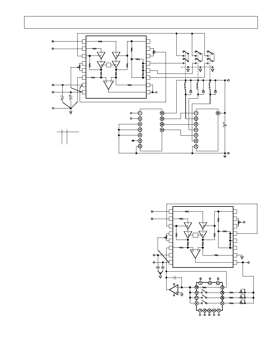
AC BRIDGE
Bridge circuits which use dc excitation are often plagued by
errors caused by thermocouple effects, l/f noise, dc drifts in the
electronics, and line noise pickup. One way to get around these
problems is to excite the bridge with an ac waveform, amplify
the bridge output with an ac amplifier, and synchronously
demodulate the resulting signal. The ac phase and amplitude
information from the bridge is recovered as a dc signal at the
output of the synchronous demodulator. The low frequency
system noise, dc drifts, and demodulator noise all get mixed to
the carrier frequency and can be removed by means of a low-
pass filter. Dynamic response of the bridge must be traded off
against the amount of attenuation required to adequately sup-
press these residual carrier components in the selection of the
filter.
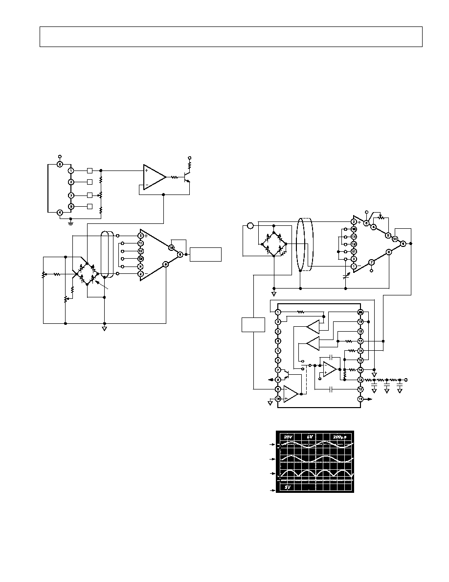
Figure 45 is an example of an ac bridge system with the AD630
used as a synchronous demodulator. The oscilloscope photo-
graph shows the results of a 0.05% bridge imbalance caused by
the 1 Meg resistor in parallel with one leg of the bridge. The top
trace represents the bridge excitation, the upper middle trace is
the amplified bridge output, the lower-middle trace is the out-
put of the synchronous demodulator and the bottom trace is the
filtered dc system output.
This system can easily resolve a 0.5 ppm change in bridge
impedance. Such a change will produce a 6.3 mV change in the
low-pass filtered dc output, well above the RTO drifts and noise.
The AC-CMRR of the AD624 decreases with the frequency of
the input signal. This is due mainly to the package-pin capaci-
tance associated with the AD624's internal gain resistors. If
AC-CMRR is not sufficient for a given application, it can be
trimmed by using a variable capacitor connected to the amplifier's
RG
2
pin as shown in Figure 45.
AD624C
≠V
S
+V
S
V
OUT
G = 1000
RG
1
RG
2
10k
1kHz
BRIDGE
EXCITATION
1M
1k
1k
1k
1k
4≠49pF
CERAMIC ac
BALANCE
CAPACITOR
≠V
10k
B
10k
5k
2.5k
≠V
S
PHASE
SHIFTER
AD630
MODULATED
OUTPUT
SIGNAL
+V
S
MODULATION
INPUT
CARRIER
INPUT
2.5k
B
A
COMP
Figure 45. AC Bridge
0V
0V
0V
0V
BRIDGE EXCITATION
(20V/div) (A)
AMPLIFIED BRIDGE
OUTPUT (5V/div) (B)
DEMODULATED BRIDGE
OUTPUT (5V/div) (C)
FILTER OUTPUT
2V/div) (D)
2V
Figure 46. AC Bridge Waveforms
REV. C
AD624
≠14≠
AD624C
≠V
S
+V
S
G = 100
RG
1
RG
2
10k
350
+10V
14-BIT
ADC
0 TO 2V
F.S.
350
350
350
Figure 47. Typical Bridge Application
Table II. Error Budget Analysis of AD624CD in Bridge Application
Effect on
Effect on
Absolute
Absolute
Effect
AD624C
Accuracy
Accuracy
on
Error Source
Specifications
Calculation
at T
A
= +25 C
at T
A
= +85 C Resolution
Gain Error
±
0.1%
±
0.1% = 1000 ppm
1000 ppm
1000 ppm
≠
Gain Instability
10 ppm
(10 ppm/
∞
C) (60
∞
C) = 600 ppm
_
600 ppm
≠
Gain Nonlinearity
±
0.001%
±
0.001% = 10 ppm
≠
≠
10 ppm
Input Offset Voltage
±
25
µ
V, RTI
±
25
µ
V/20 mV =
±
1250 ppm
1250 ppm
1250 ppm
≠
Input Offset Voltage Drift
±
0.25
µ
V/
∞
C
(
±
0.25
µ
V/
∞
C) (60
∞
C)= 15
µ
V
15
µ
V/20 mV = 750 ppm
≠
750 ppm
≠
Output Offset Voltage
1
±
2.0 mV
±
2.0 mV/20 mV = 1000 ppm
1000 ppm
1000 ppm
≠
Output Offset Voltage Drift
1
±
10
µ
V/
∞
C
(
±
10
µ
V/
∞
C) (60
∞
C) = 600
µ
V
600
µ
V/20 mV = 300 ppm
≠
300 ppm
≠
Bias Current≠Source
±
15 nA
(
±
15 nA)(5
) = 0.075
µ
V
Imbalance Error
0.075
µ
V/20mV = 3.75 ppm
3.75 ppm
3.75 ppm
≠
Offset Current≠Source
±
10 nA
(
±
10 nA)(5
) = 0.050
µ
V
Imbalance Error
0.050
µ
V/20 mV = 2.5 ppm
2.5 ppm
2.5 ppm
≠
Offset Current≠Source
±
10 nA
(10 nA) (175
) = 1.75
µ
V
Resistance Error
1.75
µ
V/20 mV = 87.5 ppm
87.5 ppm
87.5 ppm
≠
Offset Current≠Source
±
100 pA/
∞
C
(100 pA/
∞
C) (175
) (60
∞
C) = 1
µ
V
Resistance≠Drift
1
µ
V/20 mV = 50 ppm
≠
50 ppm
≠
Common-Mode Rejection
115 dB
115 dB = 1.8 ppm
◊
5 V = 9
µ
V
5 V dc
9
µ
V/20 mV = 444 ppm
450 ppm
450 ppm
≠
Noise, RTI
(0.1 Hz≠10 Hz)
0.22
µ
V p-p
0.22
µ
V p-p/20 mV = 10 ppm
_
≠
10 ppm
Total Error
3793.75 ppm
5493.75 ppm
20 ppm
NOTE
1
Output offset voltage and output offset voltage drift are given as RTI figures.
For a comprehensive study of instrumentation amplifier design
and applications, refer to the
Instrumentation Amplifier Application
Guide, available free from Analog Devices.
ERROR BUDGET ANALYSIS
To illustrate how instrumentation amplifier specifications are
applied, we will now examine a typical case where an AD624 is
required to amplify the output of an unbalanced transducer.
Figure 47 shows a differential transducer, unbalanced by
5
,
supplying a 0 to 20 mV signal to an AD624C. The output of the
IA feeds a 14-bit A to D converter with a 0 to 2 volt input volt-
age range. The operating temperature range is ≠25
∞
C to +85
∞
C.
Therefore, the largest change in temperature
T within the
operating range is from ambient to +85
∞
C (85
∞
C ≠ 25
∞
C =
60
∞
C.)
In many applications, differential linearity and resolution are of
prime importance. This would be so in cases where the absolute
value of a variable is less important than changes in value. In
these applications, only the irreducible errors (20 ppm =
0.002%) are significant. Furthermore, if a system has an intelli-
gent processor monitoring the A to D output, the addition of an
autogain/autozero cycle will remove all reducible errors and may
eliminate the requirement for initial calibration. This will also
reduce errors to 0.002%.
REV. C
AD624
≠15≠
OUTLINE DIMENSIONS
Dimensions shown in inches and (mm).
Side-Brazed Solder Lid Ceramic DIP
(D-16)
16
1
8
9
0.080 (2.03) MAX
0.310 (7.87)
0.220 (5.59)
PIN 1
0.005 (0.13) MIN
0.100
(2.54)
BSC
SEATING
PLANE
0.023 (0.58)
0.014 (0.36)
0.060 (1.52)
0.015 (0.38)
0.200 (5.08)
MAX
0.200 (5.08)
0.125 (3.18)
0.070 (1.78)
0.030 (0.76)
0.150
(3.81)
MAX
0.840 (21.34) MAX
0.320 (8.13)
0.290 (7.37)
0.015 (0.38)
0.008 (0.20)
C805d≠0≠7/99
PRINTED IN U.S.A.