/home/web/htmldatasheet/RUSSIAN/html/ad/164241
a
DC Coupled Demodulating
120 MHz Logarithmic Amplifier
AD640
One Technology Way, P.O. Box 9106, Norwood, MA 02062-9106, U.S.A.
Tel: 617/329-4700
Fax: 617/326-8703
FEATURES
Complete, Fully Calibrated Monolithic System
Five Stages, Each Having 10 dB Gain, 350 MHz BW
Direct Coupled Fully Differential Signal Path
Logarithmic Slope, Intercept and AC Response are
Stable Over Full Military Temperature Range
Dual Polarity Current Outputs Scaled 1 mA/Decade
Voltage Slope Options (1 V/Decade, 100 mV/dB, etc.)
Low Power Operation (Typically 220 mW at 5 V)
Low Cost Plastic Packages Also Available
APPLICATIONS
Radar, Sonar, Ultrasonic and Audio Systems
Precision Instrumentation from DC to 120 MHz
Power Measurement with Absolute Calibration
Wide Range High Accuracy Signal Compression
Alternative to Discrete and Hybrid IF Strips
Replaces Several Discrete Log Amp ICs
PRODUCT DESCRIPTION
The AD640 is a complete monolithic logarithmic amplifier. A
single AD640 provides up to 50 dB of dynamic range for fre-
quencies from dc to 120 MHz. Two AD640s in cascade can
provide up to 95 dB of dynamic range at reduced bandwidth.
The AD640 uses a successive detection scheme to provide an
output current proportional to the logarithm of the input volt-
age. It is laser calibrated to close tolerances and maintains high
accuracy over the full military temperature range using supply
voltages from
±
4.5 V to
±
7.5 V.
The AD640 comprises five cascaded dc coupled amplifier/lim-
iter stages, each having a small signal voltage gain of 10 dB and
a 3 dB bandwidth of 350 MHz. Each stage has an associated
full-wave detector, whose output current depends on the abso-
lute value of its input voltage. The five outputs are summed to
provide the video output (when low-pass filtered) scaled at 1 mA
per decade (50
µ
A per dB). On chip resistors can be used to
convert this output current to a voltage with several convenient
slope options. A balanced signal output at +50 dB (referred to
input) is provided to operate AD640s in cascade.
The logarithmic response is absolutely calibrated to within
±
l dB
for dc or square wave inputs from
±
0.75 mV to
±
200 mV,
with an intercept (logarithmic offset) at 1 mV dc. An integral
X10 attenuator provides an alternative input range of
±
7.5 mV
to
±
2 V dc. Scaling is also guaranteed for sinusoidal inputs.
The AD640B is specified for the industrial temperature range of
40
°
C to +85
°
C and the AD640T, available processed to MIL-
STD-883B, for the military range of 55
°
C to +125
°
C. Both are
available in 20-pin side brazed ceramic DIPs or leadless chip
carriers (LCC). The AD640J is specified for the commercial
temperature range of 0
°
C to +70
°
C, and is available in both
20-pin plastic DIP (N) and PLCC (P) packages.
This device is now available to Standard Military Drawing
(DESC) number 5962-9095501MRA and 5962-9095501M2A.
PRODUCT HIGHLIGHTS
1. Absolute calibration of a wideband logarithmic amplifier is
unique. The AD640 is a high accuracy measurement device,
not simply a logarithmic building block.
2. Advanced design results in unprecedented stability over the
full military temperature range.
3. The fully differential signal path greatly reduces the risk of
instability due to inadequate power supply decoupling and
shared ground connections, a serious problem with com-
monly used unbalanced designs.
4. Differential interfaces also ensure that the appropriate ground
connection can be chosen for each signal port. They further
increase versatility and simplify applications. The signal input
impedance is ~500 k
in shunt with ~2 pF.
5. The dc coupled signal path eliminates the need for numerous
interstage coupling capacitors and simplifies logarithmic con-
version of subsonic signals.
6. The low input offset voltage of 50
µ
V (200
µ
V max) ensures
good accuracy for low level dc inputs.
7. Thermal recovery "tails," which can obscure the response
when a small signal immediately follows a high level input,
have been minimized by special attention to design details.
8. The noise spectral density of 2 nV/
Hz
results in a noise floor of
~23
µ
V rms (80 dBm) at a bandwidth of 100 MHz. The dy-
namic range using cascaded AD640s can be extended to 95 dB
by the inclusion of a simple filter between the two devices.
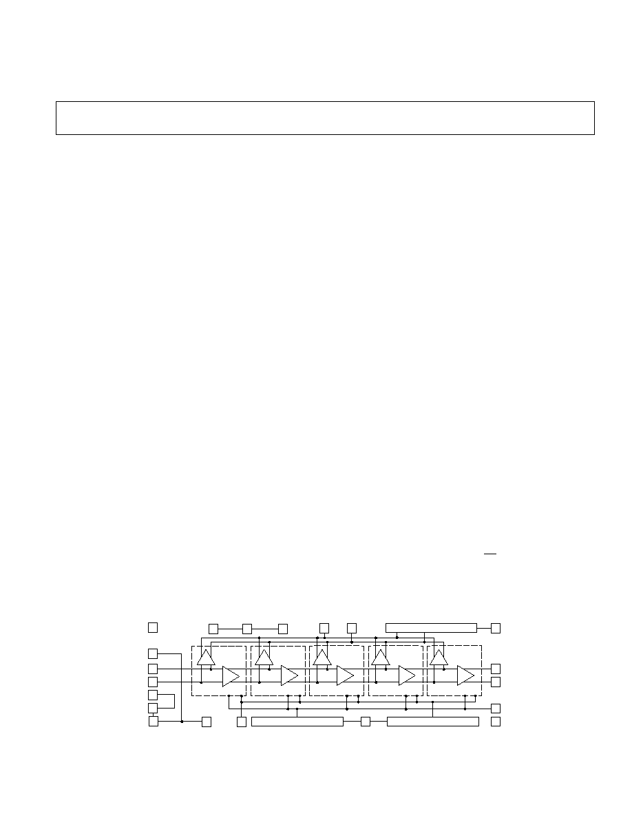
FUNCTIONAL BLOCK DIAGRAM
ATN OUT
1
20
10db
AMPLIFIER/LIMITER
FULL-WAVE
DETECTOR
2
3
ATN LO
ATN COM
10
11
SIG +IN
SIG IN
10db
AMPLIFIER/LIMITER
FULL-WAVE
DETECTOR
10db
AMPLIFIER/LIMITER
FULL-WAVE
DETECTOR
10db
AMPLIFIER/LIMITER
FULL-WAVE
DETECTOR
10db
AMPLIFIER/LIMITER
FULL-WAVE
DETECTOR
ATN COM
19
18
COM
5
27
30
270
ATN
IN
17
1k
1k
16
15
RG1
RG0
RG2
V
S
7
8
9
SLOPE BIAS REGULATOR
GAIN BIAS REGULATOR
6
BL1
4
12
INTERCEPT POSITIONING BIAS
+V
S
13
14
LOG
OUT
LOG
COM
SIG + OUT
SIG OUT
BL2
ITC
REV. A
Information furnished by Analog Devices is believed to be accurate and
reliable. However, no responsibility is assumed by Analog Devices for its
use, nor for any infringements of patents or other rights of third parties
which may result from its use. No license is granted by implication or
otherwise under any patent or patent rights of Analog Devices.

AD640SPECIFICATIONS
DC SPECIFICATIONS
Model
AD640J
AD640B
AD640T
Transfer Function
1
I
OUT
= I
Y
LOG |V
IN
/V
X
| for V
IN
=
±
0.75 mV to
±
200 mV dc
Parameter
Conditions
Min
Typ
Max
Min
Typ
Max
Min
Typ
Max
Units
SIGNAL INPUTS (Pins 1, 20)
Input Resistance
Differential
500
500
500
k
Input Offset Voltage
Differential
50
500
50
200
50
200
µ
V
vs. Temperature
0.8
0.8
0.8
µ
V/
°
C
Over Temperature
T
MIN
to T
MAX
300
µ
V
vs. Supply
2
2
2
µ
V/V
Input Bias Current
7
25
7
25
7
25
µ
A
Input Bias Offset
1
l
l
µ
A
Common-Mode Range
2
+0.3
2
+0.3
2
+0.3
V
INPUT ATTENUATOR
(Pins 2, 3, 4, 5 and 19)
Attenuation
2
Pin 5 to Pin 19
20
20
20
dB
Input Resistance
Pins 5 to 3/4
300
300
300
SIGNAL OUTPUT (Pins 10, 11)
Small Signal Gain
4
50
50
50
dB
Peak Differential Output
5
±
180
±
180
±
180
mV
Output Resistance
Either Pin to COM
75
75
75
Quiescent Output Voltage
Either Pin to COM
90
90
90
mV
LOGARITHMIC OUTPUT
6
(Pin 14)
Voltage Compliance Range
0.3
+V
S
1
0.3
+V
S
1
0.3
V
S
1
V
Slope Current, I
Y
0.95
1.00
1.05
0.98
1.00
1.02
0.98
1.00
1.02
mA
Accuracy vs. Temperature
0.002
0.002
0.002
%/
°
C
T
MIN
to T
MAX
0.98
1.02
mA
Accuracy vs. Supply
+V
S
= 4.5 V to 7.5 V
0.08
1.0
0.08
0.4
0.08
0.4
%/V
Intercept Voltage
7
, V
X
0.85
1.00
1.15
0.95
1.00
1.05
0.95
1.00
1.05
mV
vs. Temperature
0.5
0.5
0.5
µ
V/
°
C
Over Temperature
T
MIN
to T
MAX
0.90
1.10
mV
vs. Supply
±
V
S
= 4.5 V to 7.5 V
2
2
2
µ
V/V
Logarithmic Offset
(Alt. Definition of V
X
)
61.5
60.0
58.7
60.5
60.0
59.5
60.5
60.0
59.5
dBV
vs. Temperature
0.004
0.004
0.004
dB/
°
C
Over Temperature
T
MIN
to T
MAX
60.9
59.1
dB
vs. Supply
±
V
S
= 4.5 V to 7.5 V
0.017
0.017
0.017
dB/V
Intercept Voltage Using Attenuator
8.25
10.0
11.75
9.0
10.0
11.0
9.0
10.0
11.0
mV
Zero Signal Output Current
3
0.2
0.2
0.2
mA
ITC Disabled
Pin 8 to COM
0.27
0.27
0.27
mA
Maximum Output Current
2.3
2.3
2.3
mA
APPLICATIONS RESISTORS
(Pins 15, 16, 17)
1.000
0.995
1.000
1.005
0.995
1.000
1.005
k
DC LINEARITY
V
IN
±
1 mV to
±
100 mV
0.35
1.2
0.35
0.6
0.35
0.6
dB
TOTAL ABSOLUTE DC
ACCURACY
V
IN
=
±
1 mV to
±
100 mV
8
0.55
2
0.55
0.9
0.55
0.9
dB
Over Temperature
T
MIN
to T
MAX
3
1.7
1.8
dB
Over Supply Range
±
V
S
= 4.5 V to 7.5 V
2
1.0
1.0
dB
V
IN
=
±
0.75 mV to
±
200 mV
1.0
3
1.0
2.0
1.0
2.0
dB
Using Attenuator
V
IN
=
±
10 mV to
±
1 V
0.4
2.5
0.4
1.5
0.4
1.5
dB
Over Temperature
T
MIN
to T
MAX
0.6
3
0.6
2.0
0.6
2.0
dB
V
IN
=
±
7.5 mV to 2 V
1.2
3.5
1.2
2.5
1.2
2.5
dB
POWER REQUIREMENTS
Voltage Supply Range
4.5
7.5
4.5
7.5
4.5
7.5
V
Quiescent Current
9
+V
S
(Pin 12)
T
MIN
to T
MAX
9
15
9
15
9
15
mA
V
S
(Pin 7)
T
MIN
to T
MAX
35
60
35
60
35
60
mA
2
REV. A
(V
S
= 5 V, T
A
= +25 C, unless otherwise noted)

AC SPECIFICATIONS
Model
AD640J
AD640B
AD640T
Parameter
Conditions
Min
Typ
Max
Min
Typ
Max
Min
Typ
Max
Units
SIGNAL INPUTS (Pins 1, 20)
Input Capacitance
Either Pin to COM
2
2
2
pF
Noise Spectral Density
1 kHz to 10 MHz
2
2
2
nV/
Hz
Tangential Sensitivity
BW = 100 MHz
72
72
72
dBm
3 dB BANDWIDTH
Each Stage
350
350
350
MHz
All Five Stages
Pins 1 & 20 to 10 & 11
145
145
145
MHz
LOGARITHMIC OUTPUTS
6
Slope Current, I
Y
f< = 1 MHz
0.96
1.0
1.04
0.98
1.0
1.02
0.98
1.0
1.02
mA
f = 30 MHz
0.88
0.94
1.00
0.91
0.94
0.97
0.91
0.94
0.97
mA
f = 60 MHz
0.82
0.90
0.98
0.86
0.90
0.94
0.86
0.90
0.94
mA
f = 90 MHz
0.88
0.88
0.88
mA
f = 120 MHz
0.85
0.85
0.85
mA
Intercept, Dual AD640s
10, 11
f< = 1 MHz
90.6
88.6
86.6
89.6
88.6
87.6
89.6
88.6
87.6
dBm
f = 30 MHz
87.6
87.6
87.6
dBm
f = 60 MHz
86.3
86.3
86.3
dBm
f = 90 MHz
83.9
83.9
83.9
dBm
f = 120 MHz
80.3
80.3
80.3
dBm
AC LINEARITY
40 dBm to 2 dBm
12
f = 1 MHz
0.5
2.0
0.5
1.0
0.5
1.0
dB
35 dBm to 10 dBm
12
f = 1 MHz
0.25
1.0
0.25
0.5
0.25
0.5
dB
75 dBm to 0 dBm
10
f = 1 MHz
0.75
3.0
0.75
1.5
0.75
1.5
dB
70 dBm to 10 dBm
10
f = 1 MHz
0.5
2.0
0.5
1.0
0.5
1.0
dB
75 dBm to +15 dBm
13
f = 10 kHz
0.5
3.0
0.5
1.5
0.5
1.5
dB
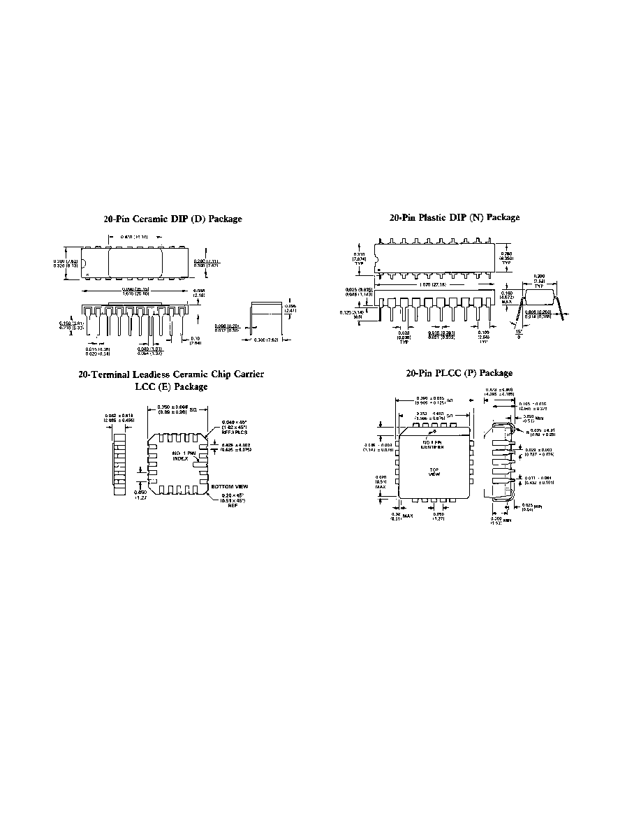
PACKAGE OPTION
20-Pin Ceramic DIP Package (D)
AD640BD
AD640TD
20-Pin Leadless Ceramic Chip Carrier (E)
AD640BE
AD640TE
20-Pin Plastic DIP Package (N)
AD640]N
20-Pin Plastic Leadless Chip Carrier (P)
AD640JP
AD640BP
NUMBER OF TRANSISTORS
155
155
1 5 5
1 5 5
NOTES
1
Logarithms to base 10 are used throughout. The response is independent of the sign of V
IN
.
2
Attenuation ratio trimmed to calibrate intercept to 10 mV when in use. It has a temperature coefficient of +0.30%/
°
C.
3
The zero-signal current is a function of temperature unless internal temperature compensation (ITC) pin is grounded.
4
Overall gain is trimmed using a
±
200
µ
V square wave at 2 kHz, corrected for the onset of compression.
5
The fully limited signal output will appear to be a square wave; its amplitude is proportional to absolute temperature.
6
Currents defined as flowing into Pin 14. See FUNDAMENTALS OF LOGARITHMIC CONVERSION for full explanation of scaling concepts. Slope is measured
by linear regression over central region of transfer function.
7
The logarithmic intercept in dBV (decibels relative to 1 V) is defined as 20 LOG
10
(V
X
/1 V).
8
Operating in circuit of Figure 24 using
±
0.1% accurate values for R
LA
and R
LB.
Includes slope and nonlinearity errors. Input offset errors also included for
V
IN
>3 mV dc, and over the full input range in ac applications.
9
Essentially independent of supply voltages.
10
Using the circuit of Figure 27, using cascaded AD640s and offset nulling. Input is sinusoidal, 0 dBm in 50
= 223 mV rms.
11
For a sinusoidal signal (see EFFECT OF WAVEFORM ON INTERCEPT). Pin 8 on second AD640 must be grounded to ensure temperature stability of intercept
for dual AD640 system.
12
Using the circuit of Figure 24, using single AD640 and offset nulling. Input is sinusoidal, 0 dBm in 50
= 223 mV rms.
13
Using the circuit of Figure 32, using cascaded AD640s and attenuator. Square wave input.
All min and max specifications are guaranteed, but only those in boldface are 100% tested on all production units. Results from those tests are used to calculate
outgoing quality levels.
Specifications subject to change without notice.
THERMAL CHARACTERISTICS
JC
( C/W)
JA
( C/W)
20-Pin Ceramic DIP Package (D-20)
25
85
20-Pin Leadless Ceramic Chip Carrier (E-20A)
25
85
20-Pin Plastic DIP Package (N-20)
24
61
20-Pin Plastic Leadless Chip Carrier (P-20A)
28
75
AD640
REV. A
3
(V
S
= 5 V, T
A
= +25 C, unless otherwise noted)
AD640
REV. A
4
ABSOLUTE MAXIMUM RATINGS*
Supply Voltage . . . . . . . . . . . . . . . . . . . . . . . . . . . . . . . .
±
7.5 V
Input Voltage (Pin 1 or Pin 20 to COM) . . . . 3 V to +300 mV
Attenuator Input Voltage (Pin 5 to Pin 3/4) . . . . . . . . . . .
±
4 V
Storage Temperature Range D, E . . . . . . . . . 65
°
C to +150
°
C
Storage Temperature Range N, P . . . . . . . . . 65
°
C to +125
°
C
Ambient Temperature Range, Rated Performance
Industrial, AD640B . . . . . . . . . . . . . . . . . . . 40
°
C to +85
°
C
Military, AD640T . . . . . . . . . . . . . . . . . . . 55
°
C to +125
°
C
Commercial, AD640J . . . . . . . . . . . . . . . . . . . 0
°
C to +70
°
C
Lead Temperature Range (Soldering 60 sec) . . . . . . . . +300
°
C
*Stresses above those listed under "Absolute Maximum Ratings" may cause
permanent damage to the device. This is a stress rating only and functional
operation of the device at these or any other conditions above those indicated in the
operational section of this specification is not implied. Exposure to absolute
maximum rating conditions for extended periods may affect device reliability.
CHIP DIMENSIONS AND
BONDING DIAGRAM
Dimensions shown in inches and (mm).
ORDERING GUIDE
Temperature
Package
Package
Model
Range
Description
Option
AD640JN
0
°
C to +70
°
C
Plastic DIP
N-20
AD640JP
0
°
C to +70
°
C
Plastic Leaded Chip
P-20A
Carrier
AD640BD
40
°
C to +85
°
C
Side Brazed Ceramic DIP D-20
AD640BE
40
°
C to +85
°
C
Ceramic Leadless Chip
E-20A
Carrier
AD640BP
40
°
C to +85
°
C
Plastic Leaded Chip
P-20A
Carrier
AD640TD/883B
55
°
C to +125
°
C Side Brazed Ceramic DIP D-20
5962-9095501MRA
AD640TE/883B
55
°
C to +125
°
C Ceramic Leadless Chip
E-20A
5962-9095501M2A
Carrier
AD640TCHIP
55
°
C to +125
°
C Chip
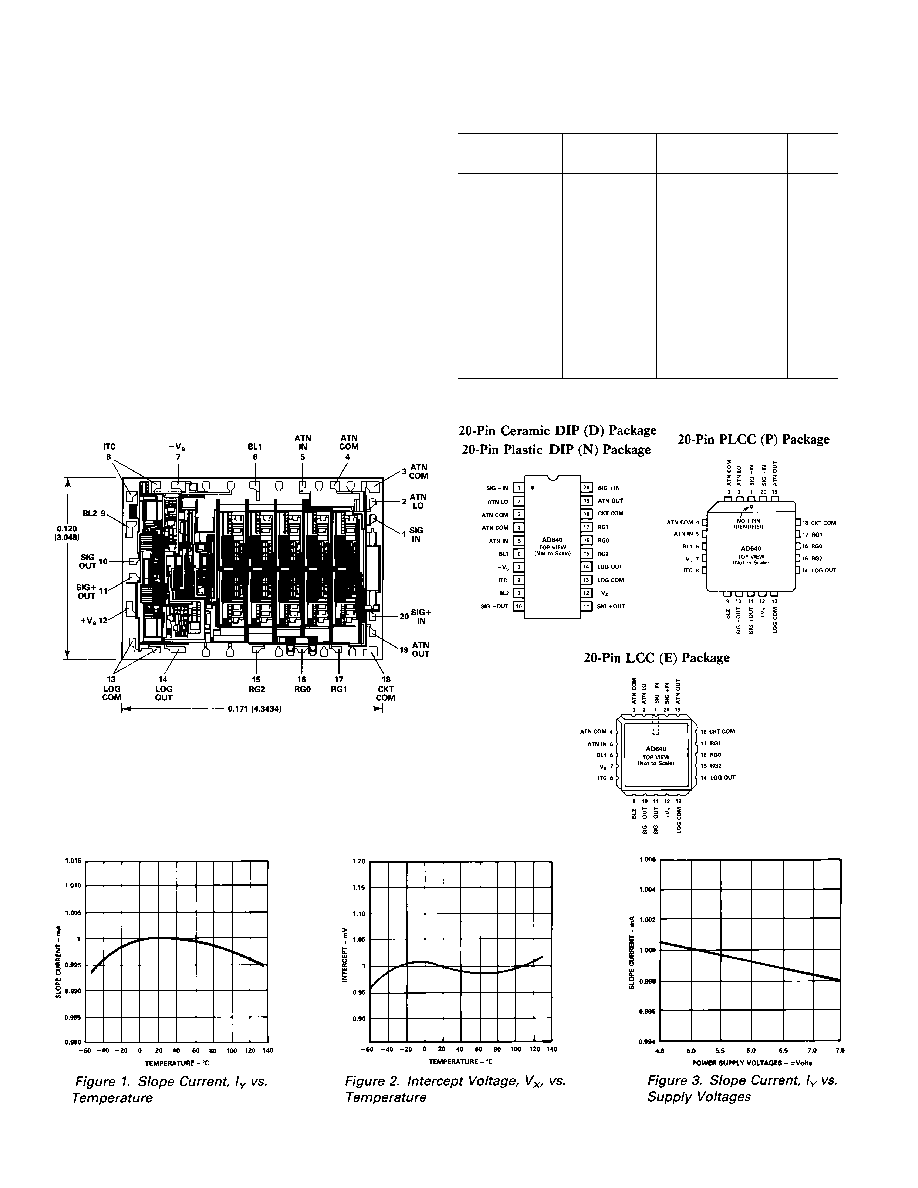
CONNECTION DIAGRAM
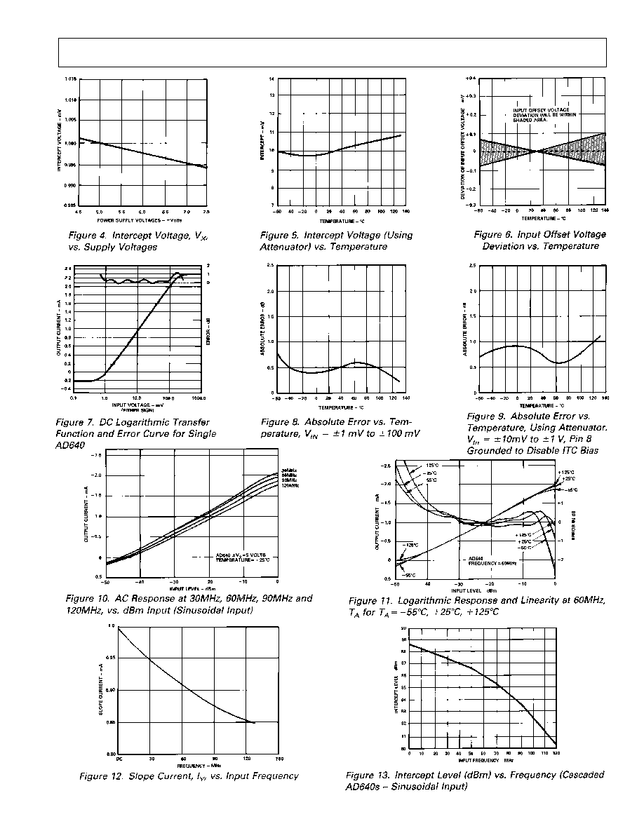
Typical Performance
(DC: Figures 19, AC: Figures 1015)
Typical PerformanceAD640
REV. A
5
AD640
REV. A
6
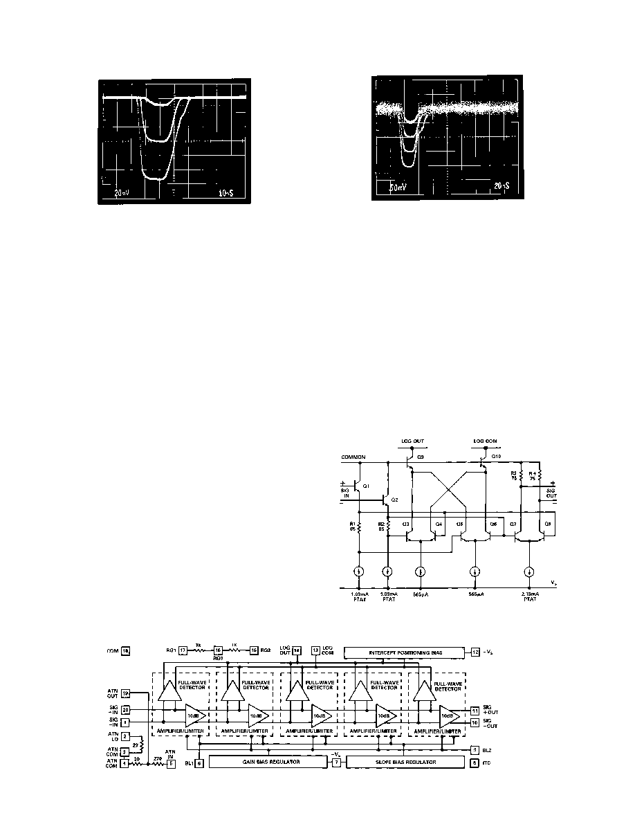
Figure 14. Baseband Pulse Response of Single AD640,
Inputs of 1 mV, 10 mV and 100 mV
CIRCUIT DESCRIPTION
The AD640 uses five cascaded limiting amplifiers to approxi-
mate a logarithmic response to an input signal of wide dynamic
range and wide bandwidth. This type of logarithmic amplifier
has traditionally been assembled from several small scale ICs
and numerous external components. The performance of these
semidiscrete circuits is often unsatisfactory. In particular, the
logarithmic slope and intercept (see FUNDAMENTALS OF
LOGARITHMIC CONVERSION) are usually not very stable
in the presence of supply and temperature variations even after
laborious and expensive individual calibration. The AD640 em-
ploys high precision analog circuit techniques to ensure stability
of scaling over wide variations in supply voltage and tempera-
ture. Laser trimming, using ac stimuli and operating conditions
similar to those encountered in practice, provides fully calibrated
logarithmic conversion.
Each of the amplifier/limiter stages in the AD640 has a small
signal voltage gain of 10 dB (
×
3.162) and a 3 dB bandwidth of
350 MHz. Fully differential direct coupling is used throughout.
This eliminates the many interstage coupling capacitors usually
required in ac applications, and simplifies low frequency signal
processing, for example, in audio and sonar systems. The
AD640 is intended for use in demodulating applications. Each
stage incorporates a detector (a full wave transconductance
rectifier) whose output current depends on the absolute value of
its input voltage.
Figure 16 is a simplified schematic of one stage of the AD640.
All transistors in the basic cell operate at near zero collector to
base voltage and low bias currents, resulting in low levels of
thermally induced distortion. These arise when power shifts
from one set of transistors to another during large input signals.
Rapid recovery is essential when a small signal immediately fol-
lows a large one. This low power operation also contributes sig-
nificantly to the excellent long-term calibration stability of the
AD640.
Figure 15. Baseband Pulse Response of Cascaded
AD640s, at Inputs of 0.2 mV, 2 mV, 20 mV and 200 mV
The complete AD640, shown in Figure 17, includes two bias
regulators. One determines the small signal gain of the amplifier
stages; the other determines the logarithmic slope. These bias
regulators maintain a high degree of stability in the resulting
function by compensating for potentially large uncertainties
in transistor parameters, temperature and supply voltages. A
third biasing block is used to accurately control the logarithmic
intercept.
By summing the signals at the output of the detectors, a good
approximation to a logarithmic transfer function can be achieved.
The lower the stage gain, the more accurate the approximation,
but more stages are then needed to cover a given dynamic
range. The choice of 10 dB results in a theoretical periodic de-
viation or ripple in the transfer function of
±
0.15 dB from the
ideal response when the input is either a dc voltage or a square
wave. The slope of the transfer function is unaffected by the in-
put waveform; however, the intercept and ripple are waveform
Figure 16. Simplified Schematic of a Single AD640 Stage
Figure 17. Block Diagram of the Complete AD640
AD640
REV. A
7
dependent (see EFFECT OF WAVEFORM ON INTERCEPT).
The input will usually be an amplitude modulated sinusoidal
carrier. In these circumstances the output is a fluctuating cur-
rent at twice the carrier frequency (because of the full wave
detection) whose average value is extracted by an external low-
pass filter, which recovers a logarithmic measure of the baseband
signal.
Circuit Operation
With reference to Figure 16, the transconductance pair Q7, Q8
and load resistors R3 and R4 form a limiting amplifier having a
small signal gain of 10 dB, set by the tail current of nominally
2.18 mA at 27
°
C. This current is basically proportional to abso-
lute temperature (PTAT) but includes additional current to
compensate for finite beta and junction resistance. The limiting
output voltage is
±
180 mV at 27
°
C and is PTAT. Emitter fol-
lowers Q1 and Q2 raise the input resistance of the stage, provide
level shifting to introduce collector bias for the gain stage and
detectors, reduce offset drift by forming a thermally balanced
quad with Q7 and Q8 and generate the detector biasing across
resistors R1 and R2.
Transistors Q3 through Q6 form the full wave detector, whose
output is buffered by the cascodes Q9 and Q10. For zero input
Q3 and Q5 conduct only a small amount (a total of about
32
µ
A) of the 565
µ
A tail currents supplied to pairs Q3Q4 and
Q5Q6. This "pedestal" current flows in output cascode Q9 to
the LOG OUT node (Pin 14). When driven to the peak output
of the preceding stage, Q3 or Q5 (depending on signal polarity)
conducts lost of the tail current, and the output rises to 532
µ
A.
The LOG OUT current has thus changed by 500
µ
A as the in-
put has changed from zero to its maximum value. Since the
detectors are spaced at 10 dB intervals, the output increases by
50
µ
A/dB, or 1 mA per decade. This scaling parameter is
trimmed to absolute accuracy using a 2 kHz square wave. At
frequencies near the system bandwidth, the slope is reduced due
to the reduced output of the limiter stages, but it is still rela-
tively insensitive to temperature variations so that a simple ex-
ternal slope adjustment in restore scaling accuracy.
The intercept position bias generator (Figure 17) removes the
pedestal current from the summed detector outputs. It is ad-
justed during manufacture such that the output (flowing into
Pin 14) is 1 mA when a 2 kHz square-wave input of exactly
±
10 mV is applied to the AD640. This places the dc intercept at
precisely 1 mV. The LOG COM output (Pin 13) is the comple-
ment of LOG OUT. It also has a 1 mV intercept, but with an
inverted slope of 1 mA/decade. Because its pedestal is very
large (equivalent to about 100 dB), its intercept voltage is not
guaranteed. The intercept positioning currents include a special
internal temperature compensation (ITC) term which can be
disabled by connecting Pin 8 to ground.
The logarithmic function of the AD640 is absolutely calibrated
to within
±
0.3 dB (or
±
15
µ
A) for 2 kHz square-wave inputs of
±
1 mV to
±
l00 mV, and to within
±
1 dB between
±
750
µ
V and
±
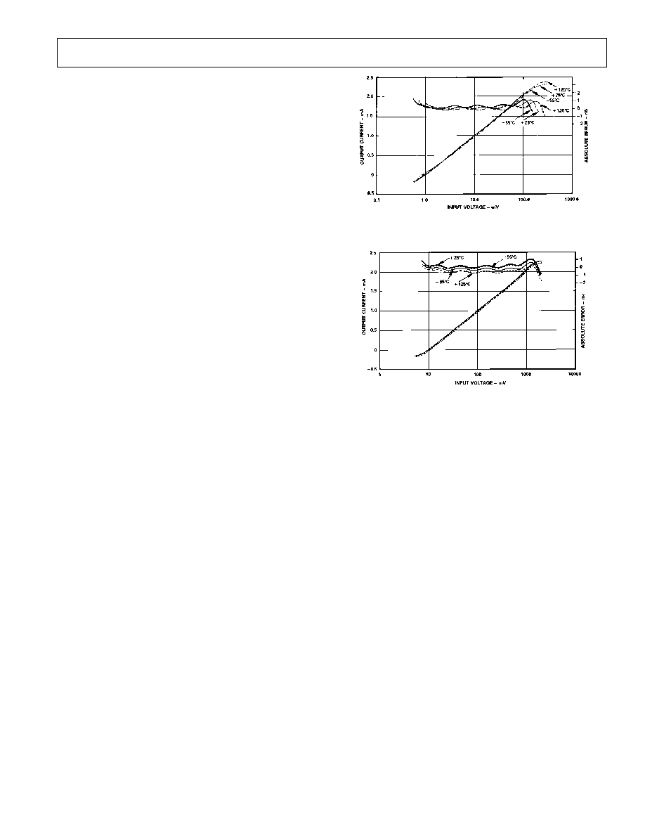
200 mV. Figure 18 is a typical plot of the dc transfer function,
showing the outputs at temperatures of 55
°
C, +25
°
C and
+125
°
C. While the slope and intercept are seen to be little af-
fected by temperature, there is a lateral shift in the endpoints of
the "linear" region of the transfer function, which reduces the
effective dynamic range. The cause of this shift is explained
FUNDAMENTALS OF LOGARITHMIC CONVERSION.
Figure 18. Logarithmic Output and Absolute Error vs. DC
or Square Wave Input at T
A
= 55
°
C, +25
°
C, Input Direct
to Pins 1 and 20
Figure 19. Logarithmic Output and Absolute Error vs. DC
or Square Wave Input at T
A
= 55
°
C, +25
°
C, +85
°
C and
+125
°
C, Input via On-Chip Attenuator
The on chip attenuator can be used to handle input levels 20 dB
higher, that is, from
±
7.5 mV to
±
2 V for dc or square wave
inputs. It is specially designed to have a positive temperature
coefficient and is trimmed to position the intercept at 10 mV dc
(or 24 dBm for a sinusoidal input) over the full temperature
range. When using the attenuator the internal bias compensa-
tion should be disabled by grounding Pin 8. Figure 19 shows
the output at 55
°
C, +25
°
C, +85
°
C and +125
°
C for a single
AD640 with the attenuator in use; the curves overlap almost
perfectly, and the lateral shift in the transfer function does not
occur. Therefore, the full dynamic range is available at all
temperatures.
The output of the final limiter is available in differential form at
Pins 10 and 11. The output impedance is 75
to ground from
either pin. For most input levels, this output will appear to have
roughly a square waveform. The signal path may be extended
using these outputs (see OPERATION OF CASCADED
AD640s). The logarithmic outputs from two or more AD640s
can be directly summed with full accuracy.
A pair of 1 k
applications resistors, RG1 and RG2 (Figure 17)
are accessed via Pins 15, 16 and 17. These can be used to con-
vert an output current to a voltage, with a slope of 1 V/decade
(using one resistor), 2 V/decade (both resistors in series) or
0.5 V/decade (both in parallel). Using all the resistors from two
AD640s (for example, in a cascaded configuration) ten slope
options from 0.25 V to 4 V/decade are available.
FUNDAMENTALS OF LOGARITHMIC CONVERSION
The conversion of a signal to its equivalent logarithmic value in-
volves a nonlinear operation, the consequences of which can be
very confusing if not fully understood. It is important to realize
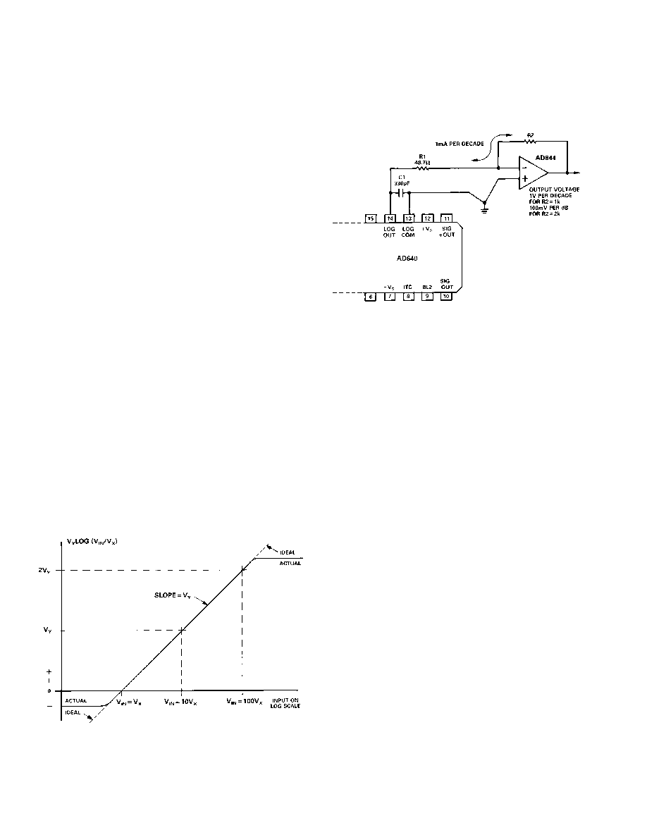
AD640
REV. A
8
from the outset that many of the familiar concepts of linear cir-
cuits are of little relevance in this context. For example, the in-
cremental gain of an ideal logarithmic converter approaches
infinity as the input approaches zero. Further, an offset at the
output of a linear amplifier is simply equivalent to an offset at
the input, while in a logarithmic converter it is equivalent to a
change of amplitude at the input--a very different relationship.
We assume a dc signal in the following discussion to simplify the
concepts; ac behavior and the effect of input waveform on cali-
bration are discussed later. A logarithmic converter having a
voltage input V
IN
and output V
OUT
must satisfy a transfer func-
tion of the form
V
OUT
= V
Y
LOG (V
IN
/V
X
)
Equation (1)
where Vy and Vx are fixed voltages which determine the scaling
of the converter. The input is divided by a voltage because the
argument of a logarithm has to be a simple ratio. The logarithm
must be multiplied by a voltage to develop a voltage output.
These operations are not, of course, carried out by explicit com-
putational elements, but are inherent in the behavior of the con-
verter. For stable operation, V
X
and V
Y
must be based on sound
design criteria and rendered stable over wide temperature and
supply voltage extremes. This aspect of RF logarithmic amplifier
design has traditionally received little attention.
When V
IN
= V
X
, the logarithm is zero. V
X
is, therefore, called
the Intercept Voltage, because a graph of V
OUT
versus LOG (V
IN
)
--ideally a straight line--crosses the horizontal axis at this point
(see Figure 20). For the AD640, V
X
is calibrated to exactly
1 mV. The slope of the line is directly proportional to V
Y
. Base
10 logarithms are used in this context to simplify the relation-
ship to decibel values. For V
IN
= 10 V
X
, the logarithm has a
value of 1, so the output voltage is V
Y
. At V
IN
= 100 V
X
, the
output is 2 V
Y
, and so on. V
Y
can therefore be viewed either as
the Slope Voltage or as the Volts per Decade Factor.
The AD640 conforms to Equation (1) except that its two out-
puts are in the form of currents, rather than voltages:
I
OUT
= I
Y
LOG (V
IN
/V
X
)
Equation (2)
Figure 20. Basic DC Transfer Function of the AD640
I
Y
the Slope Current, is 1 mA. The current output can readily be
converted to a voltage with a slope of 1 V/decade, for example,
using one of the 1 k
resistors provided for this purpose, in con-
junction with an op amp, as shown in Figure 21.
Figure 21. Using an External Op Amp to Convert the
AD640 Output Current to a Buffered Voltage Output
Intercept Stabilization
Internally, the intercept voltage is a fraction of the thermal volt-
age kT/q, that is, V
X
= V
XO
T/T
O
, where V
XO
is the value of V
X
at a reference temperature T
O
. So the uncorrected transfer func-
tion has the form
I
OUT
=I
Y
LOG (V
IN
T
O
/V
XO
T)
Equation (3)
Now, if the amplitude of the signal input V
IN
could somehow be
rendered PTAT, the intercept would be stable with tempera-
ture, since the temperature dependence in both the numerator
and denominator of the logarithmic argument would cancel.
This is what is actually achieved by interposing the on-chip at-
tenuator, which has the necessary temperature dependence to
cause the input to the first stage to vary in proportion to abso-
lute temperature. The end limits of the dynamic range are now to-
tally independent of temperature. Consequently, this is the
preferred method of intercept stabilization for applications
where the input signal is sufficiently large.
When the attenuator is not used, the PTAT variation in V
X
will result in the intercept being temperature dependent. Near
300K (27
°
C) it will vary by 20 LOG (301/300) dB/
°
C, about
0.03 dB/
°
C. Unless corrected, the whole output function would
drift up or down by this amount with changes in temperature. In
the AD640 a temperature compensating current I
Y
LOG(T/T
O
)
is added to the output. This effectively maintains a constant in-
tercept V
XO
. This correction is active in the default state (Pin 8
open circuited). When using the attenuator, Pin 8 should be
grounded, which disables the compensation current. The drift
term needs to be compensated only once; when the outputs of
two AD540s are summed, Pin 8 should be grounded on at least
one of the two devices (both if the attenuator is used).
Conversion Range
Practical logarithmic converters have an upper and lower limit
on the input, beyond which errors increase rapidly. The upper
limit occurs when the first stage in the chain is driven into limit-
ing. Above this, no further increase in the output can occur and
AD640
REV. A
9
the transfer function flattens off. The lower limit arises because
a finite number of stages provide finite gain, and therefore at
low signal levels the system becomes a simple linear amplifier.
Note that this lower limit is not determined by the intercept volt-
age, V
X
; it can occur either above or below V
X
, depending on
the design. When using two AD640s in cascade, input offset
voltage and wideband noise are the major limitations to low
level accuracy. Offset can be eliminated in various ways. Noise
can only be reduced by lowering the system bandwidth, using a
filter between the two devices.
EFFECT OF WAVEFORM ON INTERCEPT
The absolute value response of the AD640 allows inputs of
either polarity to be accepted. Thus, the logarithmic output in
response to an amplitude-symmetric square wave is a steady
value. For a sinusoidal input the fluctuating output current will
usually be low pass filtered to extract the baseband signal. The
unfiltered output is at twice the carrier frequency, simplifying the
design of this filter when the video bandwidth must be maxi-
mized. The averaged output depends on waveform in a roughly
analogous way to waveform dependence of rms value. The effect
is to change the apparent intercept voltage. The intercept volt-
age appears to be doubled for a sinusoidal input, that is, the
averaged output in response to a sine wave of amplitude (not rms
value) of 20 mV would be the same as for a dc or square wave
input of 10 mV. Other waveforms will result in different inter-
cept factors. An amplitude-symmetric-rectangular waveform
has the same intercept as a dc input, while the average of a
baseband unipolar pulse can be determined by multiplying the
response to a dc input of the same amplitude by the duty cycle.
It is important to understand that in responding to pulsed RF
signals it is the waveform of the carrier (usually sinusoidal) not
the modulation envelope, that determines the effective intercept
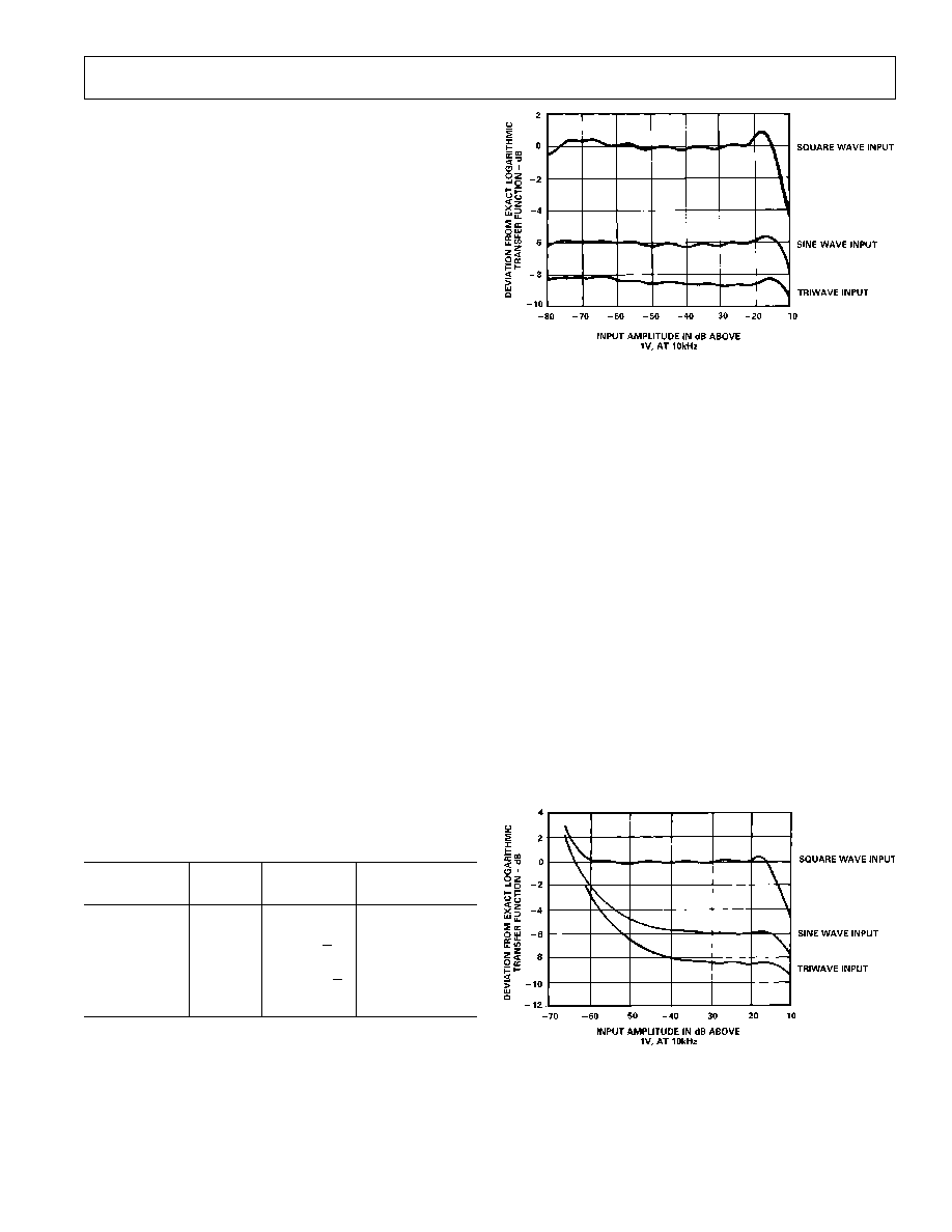
voltage. Table I shows the effective intercept and resulting deci-
bel offset for commonly occurring waveforms. The input wave-
form does not affect the slope of the transfer function. Figure 22
shows the absolute deviation from the ideal response of cascaded
AD640s for three common waveforms at input levels from
80 dBV to 10 dBV. The measured sine wave and triwave
responses are 6 dB and 8.7 dB, respectively, below the square
wave response--in agreement with theory.
Table I.
Input
Peak
Intercept
Error (Relative
Waveform
or RMS
Factor
to a DC Input)
Square Wave
Either
1
0.00 dB
Sine Wave
Peak
2
6.02 dB
Sine Wave
rms
1.414(
2
)
3.01 dB
Triwave
Peak
2.718 (e)
8.68 dB
Triwave
rms
1.569(e/
3
)
3.91 dB
Gaussian Noise
rms
1.887
5.52 dB
Logarithmic Conformance and Waveform
The waveform also affects the ripple, or periodic deviation from
an ideal logarithmic response. The ripple is greatest for dc or
square wave inputs because every value of the input voltage
maps to a single location on the transfer function and thus
traces out the full nonlinearities in the logarithmic response.
Figure 22. Deviation from Exact Logarithmic Transfer
Function for Two Cascaded AD640s, Showing Effect of
Waveform on Calibration and Linearity
By contrast, a general time varying signal has a continuum of
values within each cycle of its waveform. The averaged output is
thereby "smoothed" because the periodic deviations away from
the ideal response, as the waveform "sweeps over" the transfer
function, tend to cancel. This smoothing effect is greatest for a
triwave input, as demonstrated in Figure 22.
The accuracy at low signal inputs is also waveform dependent.
The detectors are not perfect absolute value circuits, having a
sharp "corner" near zero; in fact they become parabolic at low
levels and behave as if there were a dead zone. Consequently,
the output tends to be higher than ideal. When there are enough
stages in the system, as when two AD640s are connected in cas-
cade, most detectors will be adequately loaded due to the high
overall gain, but a single AD640 does not have sufficient gain to
maintain high accuracy for low level sine wave or triwave inputs.
Figure 23 shows the absolute deviation from calibration for the
same three waveforms for a single AD640. For inputs between
10 dBV and 40 dBV the vertical displacement of the traces for
the various waveforms remains in agreement with the predicted
dependence, but significant calibration errors arise at low signal
levels.
Figure 23. Deviation from Exact Logarithmic Transfer
Function for a Single AD640; Compare Low Level
Response with that of Figure 22
AD640
REV. A
10
SIGNAL MAGNITUDE
AD640 is a calibrated device. It is, therefore, important to be
clear in specifying the signal magnitude under all waveform con-
ditions. For dc or square wave inputs there is, of course, no am-
biguity. Bounded periodic signals, such as sinusoids and
triwaves, can be specified in terms of their simple amplitude
(peak value) or alternatively by their rms value (which is a mea-
sure of power when the impedance is specified). It is generally bet-
ter to define this type of signal in terms of its amplitude because
the AD640 response is a consequence of the input voltage, not
power. However, provided that the appropriate value of inter-
cept for a specific waveform is observed, rms measures may be
used. Random waveforms can only be specified in terms of rms
value because their peak value may be unbounded, as is the case
for Gaussian noise. These must be treated on a case-by-case ba-
sis. The effective intercept given in Table I should be used for
Gaussian noise inputs.
On the other hand, for bounded signals the amplitude can be
expressed either in volts or dBV (decibels relative to 1 V). For
example, a sine wave or triwave of 1 mV amplitude can also be
defined as an input of 60 dBV, one of 100 mV amplitude as
20 dBV, and so on. RMS value is usually expressed in dBm
(decibels above 1 mW) for a specified impedance level. Through-
out this data sheet we assume a 50
environment, the customary
impedance level for high speed systems, when referring to signal power
in dBm. Bearing in mind the above discussion of the effect of
waveform on the intercept calibration of the AD640, it will be
apparent that a sine wave at a power of, say, 10 dBm will not
produce the same output as a triwave or square wave of the
same power. Thus, a sine wave at a power level of 10 dBm has
an rms value of 70.7 mV or an amplitude of 100 mV (that is,
2
times as large, the ratio of amplitude to rms value for a sine
wave), while a triwave of the same power has an amplitude
which is
3
or 1.73 times its rms value, or 122.5 mV.
"Intercept" and "Logarithmic Offset"
If the signals are expressed in dBV, we can write the output in a
simpler form, as
I
OUT
= 50
µ
A (Input
dBV
X
dBV
) Equation (4)
where Input
dBV
is the input voltage amplitude (not rms) in dBV
and X
dBV
is the appropriate value of the intercept (for a given
waveform) in dBV. This form shows more clearly why the inter-
cept is often referred to as the logarithmic offset. For dc or square
wave inputs, V
X
is 1 mV so the numerical value of X
dBV
is 60,
and Equation (4) becomes
I
OUT
= 50
µ
A (Input
dBV
+ 60) Equation (5)
Alternatively, for a sinusoidal input measured in dBm (power in
dB above 1 mW in a 50
system) the output can be written
I
OUT
= 50
µ
A (Input
dBm
+ 44) Equation (6)
because the intercept for a sine wave expressed in volts rms is at
1.414 mV (from Table I) or 44 dBm.
OPERATION OF A SINGLE AD640
Figure 24 shows the basic connections for a single device, using
100
load resistors. Output A is a negative going voltage with a
slope of 100 mV per decade; output B is positive going with a
slope of +100 mV per decade. For applications where absolute
calibration of the intercept is essential, the main output (from
LOG OUT, Pin 14) should be used; the LOG COM output can
then be grounded. To evaluate the demodulation response, a
simple low-pass output filter having a time constant of roughly
500
µ
s (3 dB corner of 320 Hz) is provided by a 4.7
µ
F (20%
+80%) ceramic capacitor (Erie type RPE117-Z5U-475-K50V)
placed across the load. A DVM may be used to measure the av-
eraged output in verification tests. The voltage compliance at
Pins 13 and 14 extends from 0.3 V below ground up to 1 V be-
low +V
S
. Since the current into Pin 14 is from 0.2 mA at zero
signal to +2.3 mA when fully limited (dc input of >300 mV) the
output never drops below 230 mV. On the other hand, the cur-
rent out of Pin 13 ranges from 0.2 mA to +2.3 mA, and if de-
sired, a load resistor of up to 2 k
can be used on this output;
the slope would then be 2 V per decade. Use of the LOG COM
output in this way provides a numerically correct decibel read-
ing on a DVM (+100 mV = +1.00 dB).
Board layout is very important. The AD640 has both high gain
and wide bandwidth; therefore every signal path must be very
carefully considered. A high quality ground plane is essential,
but it should not be assumed that it behaves as an equipotential
plane. Even though the application may only call for modest
bandwidth, each of the three differential signal interface pairs
(SIG IN, Pins 1 and 20, SIG OUT, Pins 10 and 11, and LOG,
Pins 13 and 14) must have their own "starred" ground points to
avoid oscillation at low signal levels (where the gain is highest).
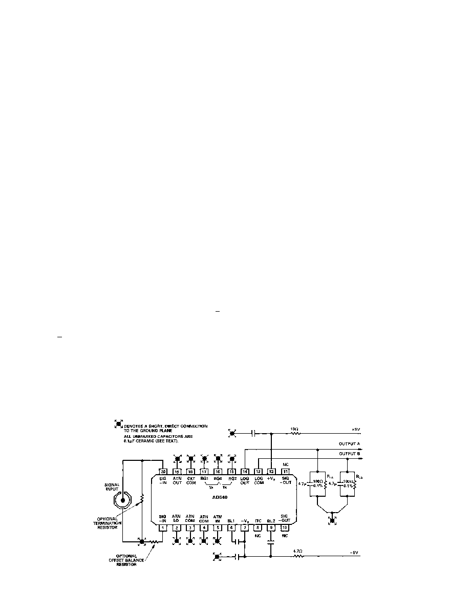
Figure 24. Connections for a Single AD640 to Verify Basic Performance
AD640
REV. A
11
Unused pins (excluding Pins 8, 10 and 11) such as the attenua-
tor and applications resistors should be grounded close to the
package edge. BL1 (Pin 6) and BL2 (Pin 9) are internal bias
lines a volt or two above the V
S
node; access is provided solely
for the addition of decoupling capacitors, which should be con-
nected exactly as shown (not all of them connect to the ground).
Use low impedance ceramic 0.1
µ
F capacitors (for example,
Erie RPE113-Z5U-105-K50V). Ferrite beads may be used in-
stead of supply decoupling resistors in cases where the supply
voltage is low.
Active Current-to-Voltage Conversion
The compliance at LOG OUT limits the available output volt-
age swing. The output of the AD640 may be converted to a
larger, buffered output voltage by the addition of an operational
amplifier connected as a current-to-voltage (transresistance)
stage, as shown in Figure 21. Using a 2 k
feedback resistor
(R2) the 50
µ
A/dB output at LOG OUT is converted to a volt-
age having a slope of +100 mV/dB, that is, 2 V per decade. This
output ranges from roughly 0.4 V for zero signal inputs to the
AD640, crosses zero at a dc input of precisely +1 mV (or
1 mV) and is +4 V for a dc input of 100 mV. A passive
prefilter, formed by R1 and C1, minimizes the high frequency
energy conveyed to the op amp. The corner frequency is here
shown as 10 MHz. The AD844 is recommended for this appli-
cation because of its excellent performance in transresistance
modes. Its bandwidth of 35 MHz (with the 2 k
feedback resis-
tor) will exceed the baseband response of the system in most ap-
plications. For lower bandwidth applications other op amps and
multipole active filters may be substituted (see, for example,
Figure 32 in the APPLICATIONS section).
Effect of Frequency on Calibration
The slope and intercept of the AD640 are calibrated during
manufacture using a 2 kHz square wave input. Calibration de-
pends on the gain of each stage being 10 dB. When the input
frequency is an appreciable fraction of the 350 MHz bandwidth
of the amplifier stages, their gain becomes imprecise and the
logarithmic slope and intercept are no longer fully calibrated.
However, the AD640 can provide very stable operation at fre-
quencies up to about one half the 3 dB frequency of the ampli-
fier stages. Figure 10 shows the averaged output current versus
input level at 30 MHz, 60 MHz, 90 MHz and 120 MHz. Fig-
ure 11 shows the absolute error in the response at 60 MHz and
at temperatures of 55
°
C, +25
°
C and +125
°
C. Figure 12 shows
the variation in the slope current, and Figure 13 shows the
variation in the intercept level (sinusoidal input) versus frequency.
If absolute calibration is essential, or some other value of slope
or intercept is required, there will usually be some point in the
user's system at which an adjustment may be easily introduced.
For example, the 5% slope deficit at 30 MHz (see Figure 12)
may be restored by a 5% increase in the value of the load resis-
tor in the passive loading scheme shown in Figure 24, or by in-
serting a trim potentiometer of 100
in series with the feedback
resistor in the scheme shown in Figure 21. The intercept can be
adjusted by adding or subtracting a small current to the output.
Since the slope current is 1 mA/decade, a 50
µ
A increment will
move the intercept by 1 dB. Note that any error in this current
will invalidate the calibration of the AD640. For example, if one
of the 5 V supplies were used with a resistor to generate the cur-
rent to reposition the intercept by 20 dB, a
±
10% variation in
this supply will cause a
±
2 dB error in the absolute calibration.
Of course, slope calibration is unaffected.
Source Resistance and Input Offset
The bias currents at the signal inputs (Pins 1 and 20) are typi-
cally 7
µ
A. These flow in the source resistances and generate in-
put offset voltages which may limit the dynamic range because
the AD640 is direct coupled and an offset is indistinguishable
from a signal. It is good practice to keep the source resistances
as low as possible and to equalize the resistance seen at each in-
put. For example, if the source resistance to Pin 20 is 100
, a
compensating resistor of 100
should be placed in series with
Pin l. The residual offset is then due to the bias current offset,
which is typically under 1
µ
A, causing an extra offset uncertainty
of 100
µ
V in this example. For a single AD640 this will rarely be
troublesome, but in some applications it may need to be nulled
out, along with the internal voltage offset component. This may
be achieved by adding an adjustable voltage of up to
±
250
µ
V at
the unused input. (Pins l and 20 may be interchanged with no
change in function.)
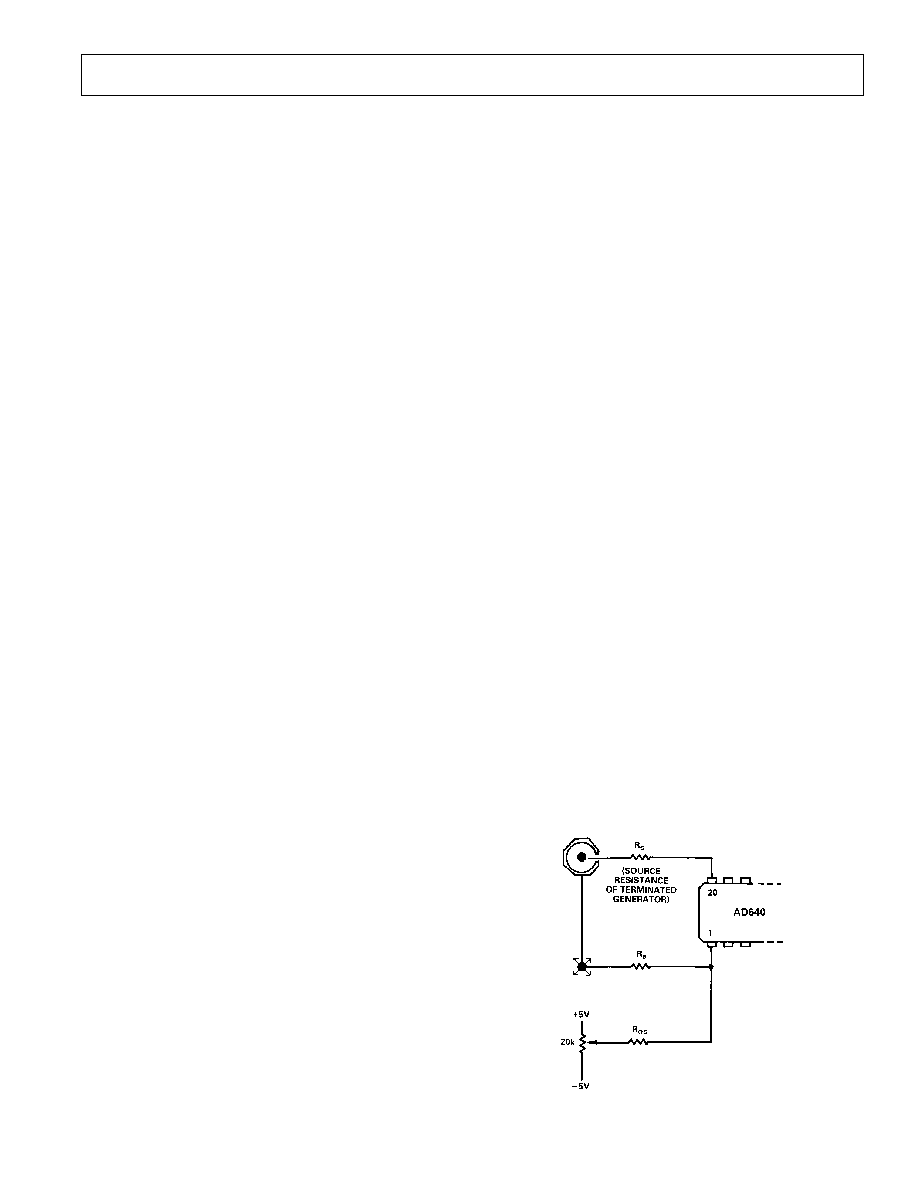
In most applications there will be no need to use any offset ad-
justment. However, a general offset trimming circuit is shown in
Figure 25. R
S
is the source resistance of the signal. Note: 50
rf
sources may include a blocking capacitor and have no dc path to
ground, or may be transformer coupled and have a near zero resis-
tance to ground. Determine whether the source resistance is zero,
25
or 50
(with the generator terminated in 50
) to find
the correct value of bias compensating resistor, R
B
, which
should optimally be equal to R
S
, unless R
S
= 0, in which case
use R
B
= 5
. The value of R
OS
should be set to 20,000R
B
to
provide a
±
250
µ
V trim range. To null the offset, set the source
voltage to zero and use a DVM to observe the logarithmic out-
put voltage. Recall that the LOG OUT current of the AD640
exhibits an absolute value response to the input voltage, so the off-
set potentiometer is adjusted to the point where the logarithmic
output "turns around" (reaches a local maximum or minimum).
At high frequencies it may be desirable to insert a coupling ca-
pacitor and use a choke between Pin 20 and ground, when Pin 1
should be taken directly to ground. Alternatively, transformer
coupling may be used. In these cases, there is no added offset
due to bias currents. When using two dc coupled AD640s (over-
all gain 100,000), it is impractical to maintain a sufficiently low
offset voltage using a manual nulling scheme. The section CAS-
CADED OPERATION explains how the offset can be auto-
matically nulled to submicrovolt levels by the use of a negative
feedback network.
Figure 25. Optional Input Offset Voltage Nulling Circuit;
See Text for Component Values
AD640
REV. A
12
Using Higher Supply Voltages
The AD640 is calibrated using
±
5 V supplies. Scaling is very in-
sensitive to the supply voltages (see dc SPECIFICATIONS)
and higher supply voltages will not directly cause significant er-
rors. However, the AD640 power dissipation must be kept be-
low 500 mW in the interest of reliability and long-term stability.
When using well regulated supply voltages above
±
6 V, the de-
coupling resistors shown in the application schematics can be
increased to maintain
±
5 V at the IC. The resistor values are
calculated using the specified maximum of 15 mA current into
the +V
S
terminal (Pin 12) and a maximum of 60 mA into the
V
S
terminal (Pin 7). For example, when using
±
9 V supplies, a
resistor of (9 V5 V)/15 mA, about 261
, should be included in
the +V
S
lead to each AD640, and (9 V5 V)/60 mA, about 64.9
,
in each V
S
lead. Of course, asymmetric supplies may be dealt
with in a similar way.
Figure 26. Details of the Input Attenuator
Using the Attenuator
In applications where the signal amplitude is sufficient, the on-
chip attenuator should be used because it provides a tempera-
ture independent dynamic range (compare Figures 18 and 19).
Figure 26 shows this attenuator in more detail. R1 is a thin-film
resistor of nominally 270
and low temperature coefficient
(TC). It is trimmed to calibrate the intercept to 10 mV dc (or
24 dBm for sinusoidal inputs), that is, to an attenuation of
nominally 20 dBs at 27
°
C. R2 has a nominal value of 30
and
has a high positive TC, such that the overall attenuation factor
is 0.33%/
°
C at 27
°
C. This results in a transmission factor that is
proportional to absolute temperature, or PTAT. (See Intercept
Stabilization for further explanation.) To improve the accuracy
of the attenuator, the ATN COM nodes are bonded to both
Pin 3 and Pin 4. These should be connected directly to the "SIG-
NAL LOW" of the source (for example, to the grounded side of
the signal connector, as shown in Figure 32) not to an arbitrary
point on the ground plane.
R4 is identical to R2, and in shunt with R3 (270
thin film)
forms a 27
resistor with the same TC as the output resistance
of the attenuator. By connecting Pin 1 to ATN LOW (Pin 2)
this resistance minimizes the offset caused by bias currents. The
offset nulling scheme shown in Figure 25 may still be used, with
the external resistor R
B
omitted and R
OS
= 500 k
. Offset sta-
bility is improved because the compensating voltage introduced
at Pin 20 is now PTAT. Drifts of under 1
µ
V/
°
C (referred to
Pins 1 and 20) can be maintained using the attenuator.
It may occasionally be desirable to attenuate the signal even
further. For example, the source may have a full-scale value of
±
10 V, and since the basic range of the AD640 extends only to
±
200 mV dc, an attenuation factor of
×
50 might be chosen.
This may be achieved either by using an independent external
attenuator or more simply by adding a resistor in series with
ATN IN (Pin 5). In the latter case the resistor must be trimmed
to calibrate the intercept, since the input resistance at Pin 5 is
not guaranteed. A fixed resistor of 1 k
in series with a 500
variable resistor calibrate to an intercept of 50 mV (or 26 dBV)
for dc or square wave inputs and provide a
±
10 V input range.
The intercept stability will be degraded to about 0.003 dB/
°
C.
Figure 27. Basic Connections for Cascaded AD640s
AD640
REV. A
13
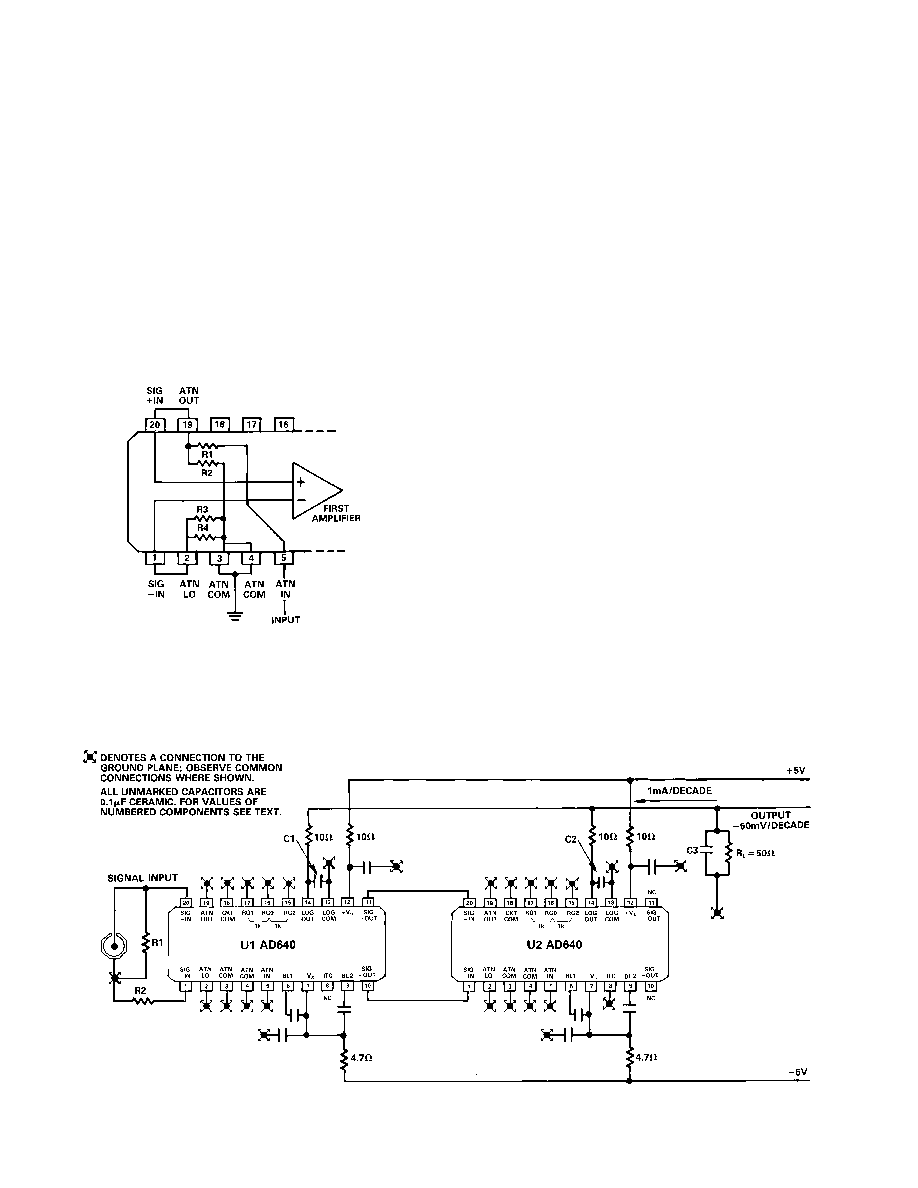
OPERATION OF CASCADED AD640S
Frequently, the dynamic range of the input will be 50 dB or
more. AD640s can be cascaded, as shown in Figure 27. The
balanced signal output from U1 becomes the input to U2. Re-
sistors are included in series with each LOG OUT pin and ca-
pacitors C1 and C2 are placed directly between Pins 13 and 14 to
provide a local path for the RF current at these output pairs. C1
through C3 are chosen to provide the required low pass corner
in conjunction with the load R
L
. Board layout and grounding
disciplines are critically important at the high gain (X100,000)
and bandwidth (~150 MHz) of this system.
The intercept voltage is calculated as follows. First, note that if
its LOG OUT is disconnected, U1 simply inserts 50 dB of gain
ahead of U2. This would lower the intercept by 50 dB, to
110 dBV for square wave calibration. With the LOG OUT of
U1 added in, there is a finite zero signal current which slightly
shifts the intercept. With the intercept temperature compensa-
tion on U1 disabled this zero signal output is 270
µ
A (see DC
SPECIFICATIONS) equivalent to a 5.4 dB upward shift in the
intercept, since the slope is 50
µ
A/dB. Thus, the intercept is at
104.6 dBV (88.6 dBm for 50
sine calibration). ITC may be
disabled by grounding Pin 8 of either U1 or U2.
Cascaded AD640s can be used in dc applications, but input off-
set voltage will limit the dynamic range. The dc intercept is 6
µ
V.
The offset should not be confused with the intercept, which is found
by extrapolating the transfer function from its central "log linear"
region. This can be understood by referring to Equation (1) and
noting that an input offset is simply additive to the value of V
IN
in the numerator of the logarithmic argument; it does not affect
the denominator (or intercept) V
X
. In dc coupled applications of
wide dynamic range, special precautions must be taken to null
the input offset and minimize drift due to input bias offset. It
is recommended that the input attenuator be used, providing
a practical input range of 74 dBV (
±
200
µ
V dc) to +6 dBV
(
±
2 V dc) when nulled using the adjustment circuit shown in
Figure 25.
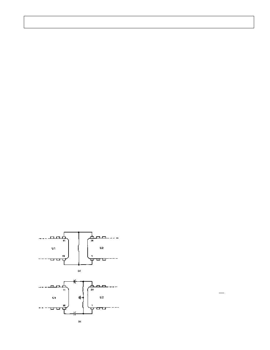
Eliminating the Effect of First Stage Offset
Usually, the input signal will be sinusoidal and U1 and U2 can
be ac coupled. Figure 28a shows a low resistance choke at the
Figure 28. Two Methods for AC Coupling AD640s
input of U2 which shorts the dc output of U1 while preserving
the hf response. Coupling capacitors may be inserted (Fig-
ure 28b) in which case two chokes are used to provide bias
paths for U2. These chokes must exhibit high impedance over
the operating frequency range.
Alternatively, the input offset can be nulled by a negative feed-
back network from the SIG OUT nodes of U2 to the SIG IN
nodes of U1, as shown in Figure 29. The low pass response of
the feedback path transforms to a closed-loop high pass re-
sponse. The high gain (
×
100,000) of the signal path results in a
commensurate reduction in the effective time constant of this
network. For example, to achieve a high pass corner of 100 kHz,
the low-pass corner must be at 1 Hz.
In fact, it is somewhat more complicated than this. When the ac
input sufficiently exceeds that of the offset, the feedback be-
comes ineffective and the response becomes essentially dc
coupled. Even for quite modest inputs the last stage will be lim-
iting and the output (Pins 10 and 11) of U2 will be a square
wave of about
±
180 mV amplitude, dwelling approximately
equal times at its two limit values, and thus having a net average
value near zero. Only when the input is very small does the high
pass behavior of this nulling loop become apparent. Consequently,
the low-pass time constant can usually be reduced considerably
without serious performance degradation.
The resistor values are chosen such that the dc feedback is ade-
quate to null the worst case input offset, say, 500
µ
V. There
must be some resistance at Pins 1 and 20 across which the offset
compensation voltage is developed. The values shown in the fig-
ure assume that we wish to terminate a 50
source at Pin 20.
The 50
resistor at Pin 1 is essential, both to minimize offsets
due to bias current mismatch and because the outputs at Pins
10 and 11 can only swing negatively (from ground to 180 mV)
whereas we need to cater for input offsets of either polarity.
For a sine input of 1
µ
V amplitude (120 dBV) and in the
absence of offset, the differential voltage at Pins 10 and 11 of
U2 would be almost sinusoidal but 100,000 times larger, or
100 mV. The last limiter in U2 would be entering saturation. A
1
µ
V input offset added to this signal would put the last limiter
well into saturation, and its output would then have a different
average value, which is extracted by the low pass network and
delivered back to the input. For larger signals, the output ap-
proaches a square wave for zero input offset and becomes rect-
angular when offset is present. The duty cycle modulation of
this output now produces the nonzero average value. Assume a
maximum required differential output of 100 mV (after averag-
ing in C1 and C2) as shown in Figure 29. R3 through R6 can
now be chosen to provide
±
500
µ
V of correction range, and with
these values the input offset is reduced by a factor of 500. Using
4.7
µ
F capacitors, the time constant of the network is about
1.2 ms, and its corner frequency is at 13.5 Hz. The closed loop
high pass corner (for small signals) is, therefore, at 1.35 MHz.
Bandwidth/Dynamic Range Tradeoffs
The first stage noise of the AD640 is 2 nV/
Hz
(short circuited
input) and the full bandwidth of the cascaded ten stages is about
150 MHz. Thus, the noise referred to the input is 24.5
µ
V rms,
or 79 dBm, which would limit the dynamic range to 77 dBs
(79 dBm to 2 dBm). In practice, the source resistances will
also generate noise, and the full bandwidth dynamic range will
be less than this.
AD640
REV. A
14
Figure 29. Feedback Offset Correction Network
A low-pass filter between U1 and U2 can limit the noise band-
width and extend the dynamic range. The simplest way to do
this is by the addition of a pair of grounded capacitors at the
signal outputs of U1 (shown as C1 and C2 in Figure 32). The
3 dB frequency of the filter must be above the highest fre-
quency to be handled by the converter; if not, nonlinearity in
the transfer function will occur. This can be seen intuitively by
noting that the system would then contract to a single AD640 at
very high frequencies (when U2 has very little input). At inter-
mediate frequencies, U2 will contribute less to the output than
would be the case if there were no interstage attenuation, result-
ing in a kink in the transfer function.
More complex filtering may be considered. For example, if the
signal has a fairly narrow bandwidth, the simple chokes shown
in Figure 28 might be replaced by one or more parallel tuned
circuits. Two separate tuned circuits or transformer coupling
should be used to eliminate all undesirable hf common mode
coupling between U1 and U2. The choice of Q for these circuits
requires compromise. Frequency sensitive nonlinearities can
arise at the edges of the band if the Q is set too high; if too low,
the transmission of the signal from U1 to U2 will be affected
even at the center frequency, again resulting in nonlinearity in
the conversion response. In calculating the Q, note that the re-
sistance from Pins 10 and 11 to ground is 75
. The input resis-
tance at Pins 1 and 20 is very high, but the capacitances at these
pins must also be factored into the total LCR circuit.
PRACTICAL APPLICATIONS
We show here two applications, using cascaded AD640s to
achieve a wide dynamic range. As already mentioned, the use of
a differential signal path and differential logarithmic outputs di-
minishes the risk of instability due to poor grounding. Neverthe-
less, it must be remembered that at high frequencies even very
small lengths of wire, including the leads to capacitors, have sig-
nificant impedance. The ground plane itself can also generate
small but troublesome voltages due to circulating currents in a
poor layout. A printed circuit evaluation board is available from
Analog Devices (Part Number ADEB640) to facilitate the
prototyping of an application using one or two AD640s, plus
various external components.
At very low signal levels various effects can cause significant de-
viation from the ideal response, apart from the inherent nonlin-
earities of the transfer function already discussed. Note that any
spurious signal presented to the AD640s is demodulated and added to
the output. Thus, in the absence of thorough shielding, emissions
from any radio transmitters or RFI from equipment operating in
the locality will cause the output to appear too high. The only
cure for this type of error is the use of very careful grounding
and shielding techniques.
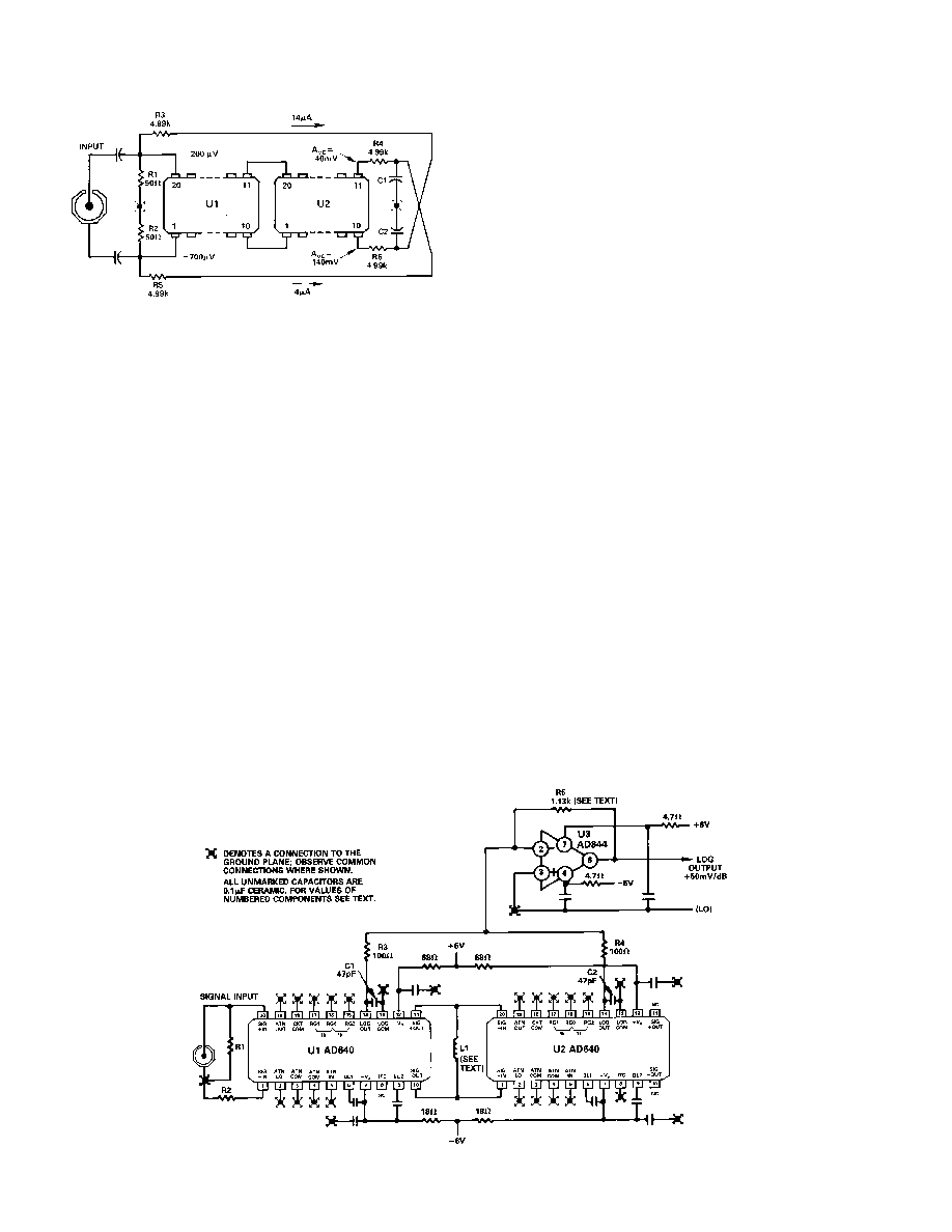
50 MHz150 MHz Converter with 70 dB Dynamic Range
Figure 30 shows a logarithmic converter using two AD640s
which can provide at least 70 dB of dynamic range, limited
mostly by first stage noise. In this application, an rf choke (L1)
prevents the transmission of dc offset from the first to the sec-
ond AD640. One or two turns in a ferrite core will generally suf-
fice for operation at frequencies above 30 MHz. For example,
one complete loop of 20 gauge wire through the two holes in a
Fair-Rite type 2873002302 core provides an inductance of 5
µ
H,
which presents an impedance of 1.57 k
at 50 MHz. The shunt-
ing effect across the 150
differential impedance at the signal
interface is thus fairly slight.
The signal source is optionally terminated by R1. To minimize
the input offset voltage R2 should be chosen to match the dc
resistance of the terminated source. (However, the offset voltage
is not a critical consideration in this ac coupled application.)
Figure 30. Complete 70 dB Dynamic Range Converter for 50 MHz150 MHz Operation
AD640
REV. A
15
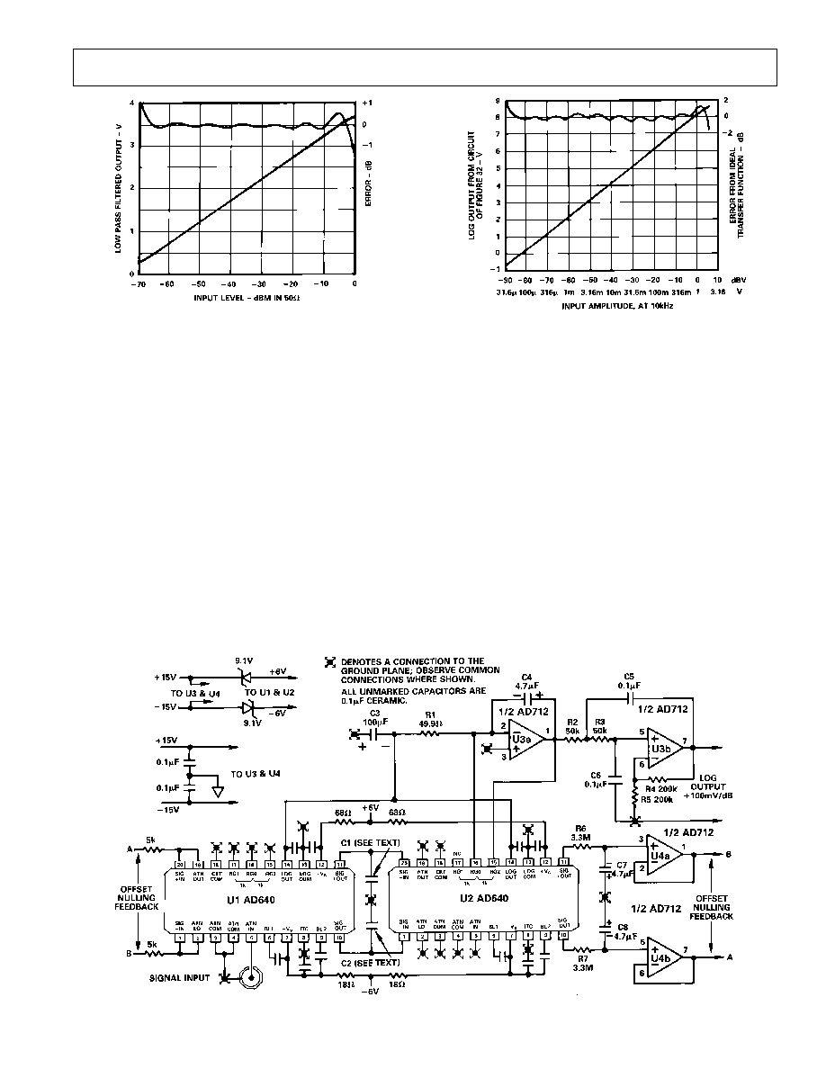
Figure 31. Logarithmic Output and Nonlinearity for Circuit
of Figure 30, for a Sine Wave Input at f = 80 MHz
Note that all unused inputs are grounded; this improves the iso-
lation from the outputs back to the inputs.
A transimpedance op amp (U3, AD844) converts the summed
logarithmic output currents of U1 and U2 to a ground referenced
voltage scaled 1 V per decade. The resistor R5 is nominally 1 k
but is increased slightly to compensate for the slope deficit at the
operating frequency, which can be determined from Figure 12.
The inverting input of U3 forms a virtual ground, so that each
logarithmic output of U1 and U2 is loaded by 100
(R3 or
R4). These resistors in conjunction with capacitors C1 and C2
form independent low pass filters with a time constant of about
5 ns. These capacitors should be connected directly across Pins
13 and 14, as shown, to prevent high frequency output currents
from circulating in the ground plane. A second 5 ns time con-
stant is formed by feedback resistor R5 in conjunction with the
transcapacitance of U3.
This filtering is adequate for input frequencies of 50 MHz or
Figure 33. Logarithmic Output and Nonlinearity for Circuit
of Figure 32, for a Square Wave Input at f = 10 kHz
above; more elaborate filtering can be devised for pulse applica-
tions requiring a faster rise time. In applications where only a
long term measure of the input is needed, C1 and C2 can be
increased and U3 can be replaced by a low speed op amp. Fig-
ure 31 shows typical performance of this converter.
10 Hz100 kHz Converter with 95 dB Dynamic Range
To increase the dynamic range it is necessary to reduce the
bandwidth by the inclusion of a low-pass filter at the signal in-
terface between U1 and U2 (Figure 32). To provide operation
down to low frequencies, dc coupling is used at the interface
between AD640s and the input offset is nulled by a feedback
circuit.
Using values of 0.02
µ
F in the interstage filter formed by capaci-
tors C1 and C2, the hf corner occurs at about l00 kHz. U3
(AD712) forms a 4-pole 35 Hz low-pass filter. This provides
operation to signal frequencies below 20 Hz. The filter response
is not critical, allowing the use of an electrolytic capacitor to
form one of the poles.
Figure 32. Complete 95 dB Dynamic Range Converter
AD640
REV. A
16
C1297a202/90
PRINTED IN U.S.A.
R1 is restricted to 50
by the compliance at Pin 14, so C3
needs to be large to form a 5 ms time constant. A tantalum
capacitor is used (note polarity). The output of U3a is scaled
+1 V per decade, and the X2 gain of U3b raises this to +2 V per
decade, or +100 mV/dB. The differential offset at the output of
U2 is low pass filtered by R6/C7 and R7/C8 and buffered by
voltage followers U4a and U4b. The 16s open loop time con-
stant translates to a closed loop high pass corner of 10 Hz. (This
high-pass filter is only operative for very small inputs; see page
13.) Figure 33 shows the performance for square wave inputs.
Since the attenuator is used, the upper end of the dynamic
range now extends to +6 dBV and the intercept is at 82 dBV.
The noise limited dynamic range is over 100 dB, but in practice
spurious signals at the input will determine the achievable range.
OUTLINE DIMENSIONS
Dimensions shown in inches and (mm).