 | ÐлекÑÑоннÑй компоненÑ: AD6432AST | СкаÑаÑÑ:  PDF PDF  ZIP ZIP |
Äîêóìåíòàöèÿ è îïèñàíèÿ www.docs.chipfind.ru
REV. 0
Information furnished by Analog Devices is believed to be accurate and
reliable. However, no responsibility is assumed by Analog Devices for its
use, nor for any infringements of patents or other rights of third parties
which may result from its use. No license is granted by implication or
otherwise under any patent or patent rights of Analog Devices.
a
AD6432
One Technology Way, P.O. Box 9106, Norwood, MA 02062-9106, U.S.A.
Tel: 617/329-4700
World Wide Web Site: http://www.analog.com
Fax: 617/326-8703
© Analog Devices, Inc., 1997
GSM 3 V Transceiver IF Subsystem
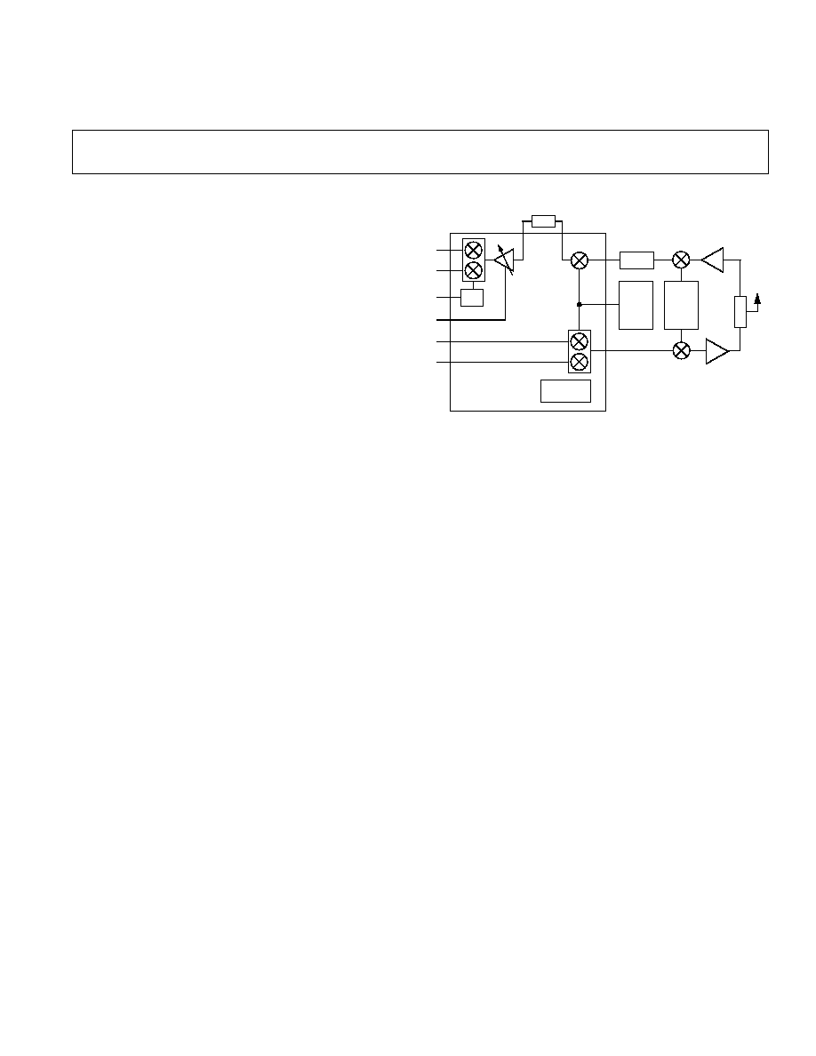
FUNCTIONAL BLOCK DIAGRAM
SAW
BP
OP AMP
AD6432
PA
RF
SYNTH
IF
SYNTH
PLO
FEATURES
Fully Compliant with Standard and Enhanced GSM
Specification
DC-350 MHz RF Bandwidths
80 dB Gain Control Range
I/Q Modulation and Demodulation
Onboard Phase Locked Tunable Oscillator
On-Chip Noise Roofing IF Filters
Ultralow Power Design
2.7 V3.6 V Operating Voltage
User-Selectable Power-Down Modes
Small 44-Lead TQFP Package
Interfaces Directly with AD20msp410 and AD20msp415
GSM Baseband Chipsets
APPLICATIONS
I/Q Modulated Digital Wireless Systems
GSM Mobile Radios
GSM PCMCIA Cards
GENERAL DESCRIPTION
The AD6432 IF IC provides the complete transmit and receive
IF signal processing, including I/Q modulation and demodula-
tion, necessary to implement a digital wireless transceiver such
as a GSM handset. The AD6432 may also be used for other
wireless TDMA standards using I/Q modulation.
The AD6432's receive signal path is based on the proven archi-
tecture of the AD607 and the AD6459. It consists of a mixer,
gain-controlled amplifiers, integrated roofing filter and I/Q
demodulators based on a PLL. The low noise, high-intercept
variable-gain mixer is a doubly-balanced Gilbert-cell type. It has
a nominal 13 dBm input-referred 1 dB compression point and
a 0 dBm input-referred third-order intercept.
The gain-control input accepts an external control voltage input
from an external AGC detector or a DAC. It provides an 80 dB
gain range with 27.5 mV/dB gain scaling, where the mixer and
the IF gains vary together.
The I and Q demodulators provide inphase and quadrature
baseband outputs to interface with Analog Devices' AD7015
and AD6421 (GSM, DCS1800, PCS1900) baseband convert-
ers. An onboard quadrature VCO, externally phase-locked to
the IF signal, drives the I and Q demodulators. The quadrature
phase-locked oscillator (QPLO) requires no external compo-
nents for frequency control or quadrature generation, and de-
modulates signals at standard GSM system IFs of 13 MHz, or
26 MHz with a reference input frequency of 13 MHz; or, in
general, 1X or 2X the reference frequency. Maximum reference
frequency is 25 MHz.
This reference signal is normally provided by an external
VCTCXO under the control of the radio's digital signal
processor. The transmit path consists of an I/Q modulator
and buffer amplifier, suitable for carrier frequencies up to
300 MHz and provides an output power of 17.5 dBm in
a 50
system. The quadrature LO signals driving the
I and Q modulator are generated internally by dividing by
two the frequency of the signal presented at the differential
LO port of the AD6432. In both the transmit and receive
paths, onboard filters provide 30 dB of stopband attenuation.
The AD6432 comes in a 44-lead plastic thin quad flatpack
(TQFP) surface mount package.

2
REV. 0
AD6432SPECIFICATIONS
(T
A
= +25 C, V
P
= 3.0 V, GREF = 1.25 V unless otherwise noted)
Parameter
Conditions
Min
Typ
Max
Units
RX RF MIXER
RF Input Frequency
350
MHz
AGC Conversion Gain Variation
Z
IN
= 150
: 0.2 V < V
GAIN
< 2.4 V
3 to +15
dB
Input 1 dB Compression Point
At V
GAIN
= 2.4 V, Z
IN
= 150
13
dBm
Input Third-Order Intercept
At V
GAIN
= 0.2 V, RF
IN
= 25 dBm
0
dBm
SSB Noise Figure
At Z
IN
= 150
, F
RF
= 246 MHz,
F
LO
= 272 MHz, V
GAIN
= 0.2 V
10
dB
RX IF AMPLIFIER
AGC Gain Variation
0.2 V < V
GAIN
< 2.4 V
14 to 48
dB
Input Resistance
at V
GAIN
= 0.2 V
5
k
Operating Frequency Range
10
50
MHz
GAIN CONTROL
Total Gain Control Range
Mixer+IF+Demod, 0.2 V < V
GAIN
< 2.4 V
80
dB
Control Voltage Range at GAIN
0.2
2.4
V
Gain Scaling
27.5
mV/dB
Gain Law Conformance
±
0.1
dB
Bias Current at GREF
0.5
µ
A
Input Resistance at Gain
20
k
INTEGRATED IF FILTER
BPF Center Frequency
f
REF
= 13 MHz
IFS0 = 1
"0" = Connect to Ground, "1" = Connect to V
P
13
MHz
IFS0 = 0
"0" = Connect to Ground, "1" = Connect to V
P
26
MHz
BPF 3 dB BW
f
REF
= 13 MHz
IFS0 = 1
"0" = Connect to Ground, "1" = Connect to V
P
5
MHz
IFS0 = 0
"0" = Connect to Ground, "1" = Connect to V
P
10
MHz
I AND Q DEMODULATOR
Demodulation Gain
17
dB
Output Voltage Range
Differential
0.3
V
POS
0.2
V
Output Voltage Common-Mode Level Not Power Supply Independent
1.5
V
Output Offset Voltage
Differential, V
GAIN
= GREF
150
+150
mV
Error in Quadrature
Differential from I to Q, IF = 13 MHz
1
3.5
Degrees
Amplitude Match
0.25
dB
I/Q Output BW
C
LOAD
= 10 pF
3
MHz
Output Resistance
Each Pin
4.7
k
QUADRATURE IF PLL
Operating Frequency Range
10
50
MHz
Reference Frequency Voltage Level
200
mV p-p
Reference Frequency Range
25
MHz
Acquisition Time
Using 1 k
, 1 nF Loop Filter
80
µ
s
TRANSMIT MODULATOR
Carrier Output Frequency
300
MHz
Output Power
R
LOAD
= 150
, Power at Final 50
,
F
IF
= 272 MHz
17.5
dBm
Input 1 dB Compression Point
R
LOAD
= 150
(Differential)
14
dBm
I/Q Input Signal Amplitude
Differential
2.056
V p-p
I/Q Input Signal Required DC Bias
1.2
V
I/Q Input BW
1
MHz
I/Q Input Resistance
100
k
I/Q Phase Balance
With LOs 2nd Harmonic 30 dBc
Bellow Fundamental
±
1.5
Degrees
I/Q Amplitude Balance
With LOs 2nd Harmonic 30 dBc
Bellow Fundamental
±
0.1
dB
Output Harmonic Content
R
LOAD
= 150
45 (3rd)
dBc
65 (5th)
dBc
Carrier Feedthrough
F
CARRIER
= 272 MHz
33
dBc
Sideband Suppression
I and Q Inputs Driven In Quadrature
37
dBc
3
REV. 0
AD6432
Parameter
Conditions
Min
Typ
Max
Units
LO PORT (LOLO and LOHI)
Input Frequency
200
600
MHz
Input Signal Voltage Range
Differential
200
mV p-p
Input Resistance
Input Pull-Up Resistors to V
POS
(Each Pin)
500
AUXILIARY OP AMPLIFIER
Small Signal 3 dB Bandwidth
50
MHz
Input Signal Voltage Range
0.1
V
POS
2.1
V
Input Offset Voltage
±
4
mV
Input Bias Current
150
nA
Output Signal Voltage Range
With R
LOAD
> 4 k
0.1
V
POS
0.2
V
POWER CONSUMPTION
Supply Voltage
2.7
3
3.6
V
Transmit Mode
13
mA
Receive Mode
At V
GAIN
= 1.2 V
13
mA
Sleep Mode
< 5
µ
A
OPERATING TEMPERATURE RANGE
25
+85
°
C
NOTES
All reference to dBm is relative to 50
.
Specifications subject to change without notice.
ABSOLUTE MAXIMUM RATINGS
1
Supply Voltage VPDV, VPPX, VPDM, VPFL, VPPC, VPRX,
to CMTX, CMRX, CMIF, CMD . . . . . . . . . . . . . . +3.6 V
Internal Power Dissipation
2
. . . . . . . . . . . . . . . . . . . 600 mW
Operating Temperature Range . . . . . . . . . . . 25
°
C to +85
°
C
Storage Temperature Range . . . . . . . . . . . . 65
°
C to +150
°
C
Lead Temperature, Soldering (60 sec) . . . . . . . . . . . +300
°
C
NOTES
1
Stresses above those listed under Absolute Maximum Ratings may cause perma-
nent damage to the device. This is a stress rating only; functional operation of the
device at these or any other conditions above those indicated in the operational
section of this specification is not implied. Exposure to absolute maximum rating
conditions for extended periods may affect device reliability.
2
Thermal Characteristics: 44-lead TQFP package:
JA
= 126
°
C.
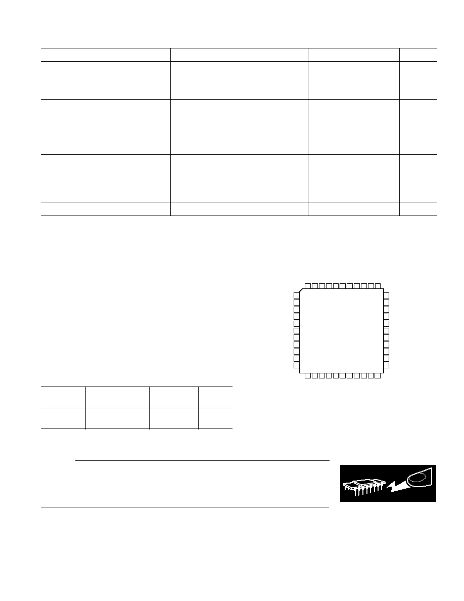
PIN CONFIGURATION
29
30
31
32
33
27
28
25
26
23
24
40 39 38
41
42
43
44
36 35 34
37
3
4
5
6
7
1
2
10
11
8
9
12 13
14 15 16 17 18 19 20 21 22
TOP VIEW
(Pins Down)
VPDV
MODO
GND
CMTX
LOLO
LOHI
CMRX
GND
RFLO
RFHI
GND
FREF
GND
IFS0
CMDM
FLTR
VPFL
VPDM
IRXP
IRXN
QRXP
QRXN
VPTX
ITXP
ITXN
QTXP
QTXN
TXPU
PCAP
PCAM
GND
VPRX
MXHI
MXLO
IFLO
IFHI
VPPC
CMIF
CMIF
RXPU
GAIN
GREF
GND
PCAO
AD6432
ORDERING GUIDE
Temperature
Package
Package
Model
Range
Description
Option*
AD6432AST
25
°
C to +85
°
C
44-Pin Plastic
ST-44
TQFP
*ST = Thin Quad Flatpack.
WARNING!
ESD SENSITIVE DEVICE
CAUTION
ESD (electrostatic discharge) sensitive device. Electrostatic charges as high as 4000 V readily
accumulate on the human body and test equipment and can discharge without detection.
Although the AD6432 features proprietary ESD protection circuitry, permanent damage may
occur on devices subjected to high energy electrostatic discharges. Therefore, proper ESD
precautions are recommended to avoid performance degradation or loss of functionality.

AD6432
4
REV. 0
PIN FUNCTION DESCRIPTIONS
Pin
Label
Description
Function
1
GND
PCB Ground
Not Bonded to IC
2
MODO
TX Modulator Output
AC Coupled, Drives 150
into 50
3
VPDV
LO2 Divided by 2 Supply Voltage
V
POS
4
CMTX
On-Chip TX Mixer Common
Ground
5
LOLO
Differential RX Mixer LO2 Input Negative
AC Coupled, V
POS
to V
POS
100 mV
6
LOHI
Differential RX Mixer LO2 Input Positive
AC Coupled, V
POS
100 mV to V
POS
7
CMRX
On-Chip RX Mixer Common
Ground
8
GND
PCB Ground
Not Bonded to IC
9
RFLO
Differential RX Mixer IF1 Input Negative
AC Coupled
10
RFHI
Differential RX Mixer IF1 Input Positive
AC Coupled
11
GND
PCB Ground
Not Bonded to IC
12
VPRX
RX Section Supply Voltage
V
POS
13
MXHI
Differential RX IF1/IF2 Mixer Output Positive
See Figure 30
14
MXLO
Differential RX IF1/IF2 Mixer Output Negative
See Figure 30
15
CMIF
On-Chip RX IF2 Common
Ground
16
IFLO
Differential RX IF2 Input Negative
AC Coupled
17
IFHI
Differential RX IF2 Input Positive
AC Coupled
18
CMIF
On-Chip RX IF2 Common
Ground
19
RXPU
RX Enable (Power-Up)
Off = Low < 0.6 V, On = High > 2.5 V
20
GAIN
RX VGA Gain Control Input
0.2 V2.4 V Using 3 V Supply. Max Gain at 0.2 V
21
GREF
RX VGA Reference Voltage
1.2 V typ
22
GND
PCB Ground
Not Bonded to IC
23
QRXN
Differential Demodulator Q Output Negative
Internal 4.7 k
Resistor in Series with the Output
24
QRXP
Differential Demodulator Q Output Positive
Internal 4.7 k
Resistor in Series with the Output
25
IRXN
Differential Demodulator I Output Negative
Internal 4.7 k
Resistor in Series with the Output
26
IRXP
Differential Demodulator I Output Positive
Internal 4.7 k
Resistor in Series with the Output
27
VPDM
Demodulator Supply Voltage
V
POS
28
VPFL
I/Q LO PLL Filter Cap. Supply Voltage
To V
POS
with Good Decoupling
29
FLTR
I/Q LO PLL Filter
Referenced to VPFL
30
CMDM
On-Chip Demodulator Common
Ground
31
IFS0
IF2 Frequency Select Bit
"0" = Low < 0.6 V, "1" = High > 2.5 V
32
GND
PCB Ground
Not Bonded to IC
33
FREF
Reference Input (13 MHz for GSM)
AC Coupled. Use 200 mV p-p Input Signal
34
VPPC
Auxiliary Op Amp Supply Voltage
V
POS
35
PCAO
Auxiliary Op Amp Output
Active when TXPU Is High
36
GND
PCB Ground
Not Bonded to IC
37
PCAM
Differential Auxiliary Op Amp Input Negative
0.1 V to V
POS
2.1 V
38
PCAP
Differential Auxiliary Op Amp Input Positive
0.1 V to V
POS
2.1 V
39
TXPU
TX Enable (Power-Up)
Low < 0.6 V, High > 2.5 V
40
QTXN
Differential Modulator Q Input Negative
DC Coupled, 1.2 V
±
514 mV
41
QTXP
Differential Modulator Q Input Positive
DC Coupled, 1.2 V
±
514 mV
42
ITXN
Differential Modulator I Input Negative
DC Coupled, 1.2 V
±
514 mV
43
ITXP
Differential Modulator I Input Positive
DC Coupled, 1.2 V
±
514 mV
44
VPTX
TX Section Supply Voltage
V
POS
AD6432
5
REV. 0
12 13
14 15 16 17 18 19 20 21 22
3
4
5
6
7
1
2
10
11
8
9
40 39 38
41
42
43
44
36 35 34
37
29
30
31
32
33
27
28
25
26
23
24
TOP VIEW
(Pins Down)
TXPU
R3
49.9
C1
100pF
R9
84
MODO
R25
1k
C29
0.1 F
R34
0
C11
0.01 F
C10
1000pF
C32
0.1 F
VS2
VPDV
DECOUPLING
VS1
R2
0
R23
123
QTXN
QTXP
ITXN
PCAP
R30
49.9
C5
0.01 F
C9
0.1 F
R11
1k
R12
0
R1
1k
R14
249
C18
0.1 F
1
2
3
R10
500
R8
0
IFS0
R32
49.9
C36
1000pF
R6
0
C41
0.01 F
C17
0.1 F
C23
0.01 F
R7
0
C6
47pF
C8
47pF
IRXP
IRXN
QRXP
QXRN
C28
0.1 F
VPTX
DECOUPLING
C14
0.01 F
C15
100pF
4
6
LOLO
ITXP
T1
VS1
RFHI
C2
100pF
R31
0
VS1
C30
0.1 F
C3
0.01 F
MXHI
MXLO
C43
0.047 F
C44
0.047 F
C4
0.047 F
R4
49.9
C7
0.047 F
R5
49.9
IFLO
IFHI
RXPU
GAIN
GREF
C39
0.01 F
C40
0.01 F
IFS0
RXPU
VS1
GND
C7
4.7 F
GAIN
GREF
TXPU
C7
4.7 F
J1
J3
J4
J5
VS2
VS1
PCAO
FREF
VS1
VPDV
MODO
GND
CMTX
LOLO
LOHI
CMRX
GND
RFLO
RFHI
GND
FREF
GND
IFS0
CMDM
FLTR
VPFL
VPDM
IRXP
IRXN
QRXP
QRXN
VPTX
ITXP
ITXN
QTXP
QTXN
TXPU
PCAP
PCAM
GND
VPRX
MXHI
MXLO
IFLO
IFHI
VPPC
CMIF
CMIF
RXPU
GAIN
GREF
GND
PCAO
AD6432
VPPC
DECOUPLING
R39
OPEN
PCAM
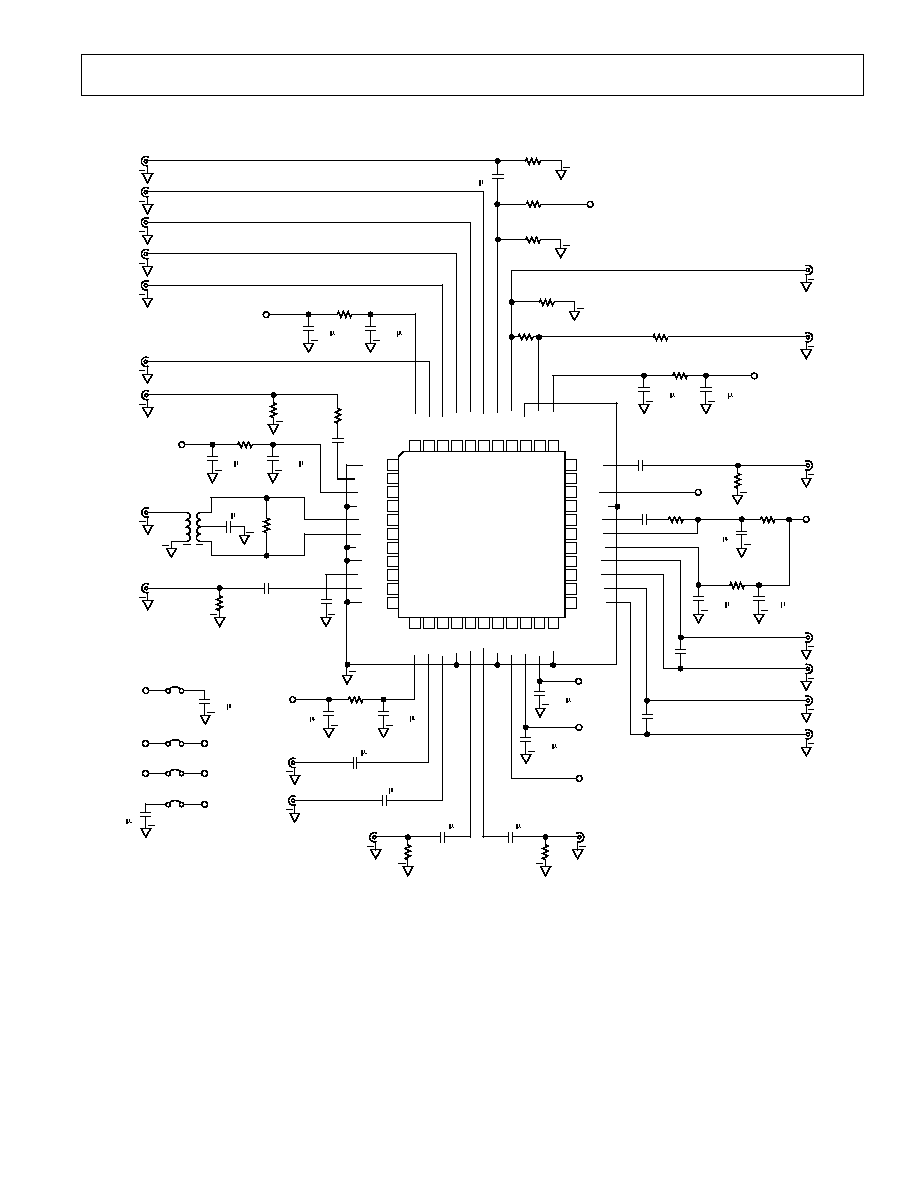
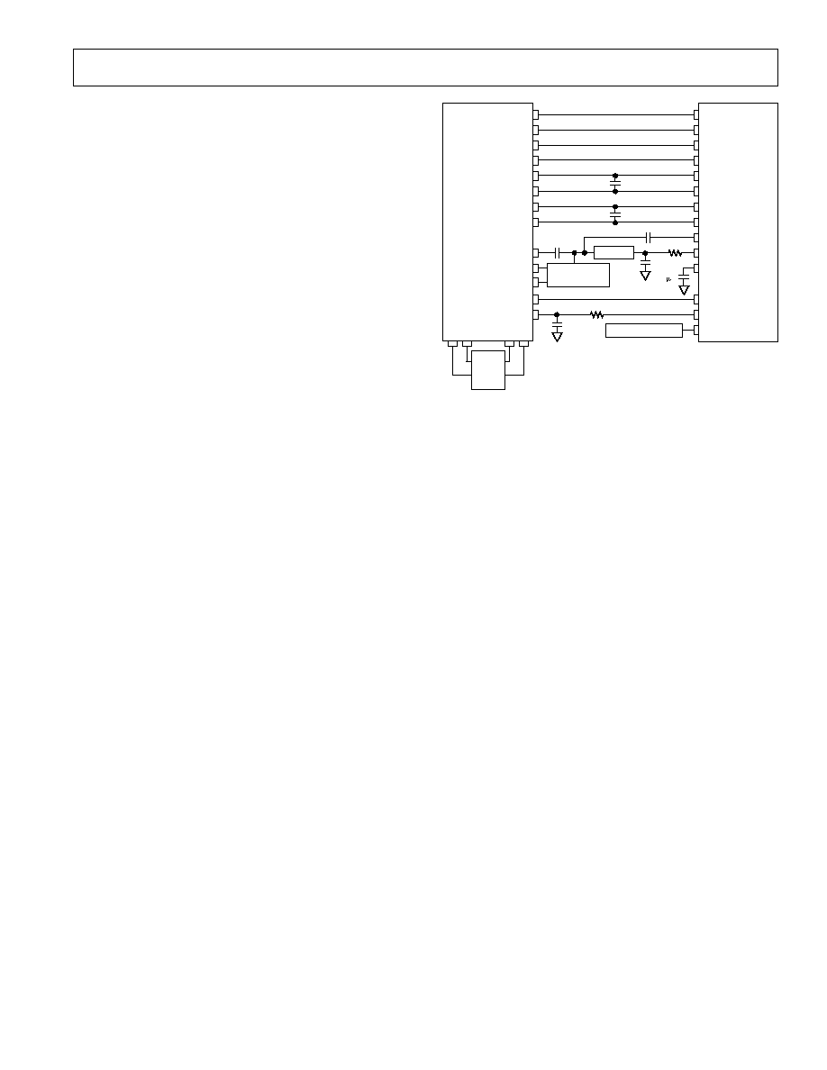
Figure 1. Characterization Board
AD6432
6
REV. 0
3
1
2
TXPU
ITX
QTX
MODO
LOIP
RFHI
MXOUT
VS1
VS2
GND
VP
VN
GAIN
IFIN
FREF
IRX
QRX
PCAP
PCAO
3
1
2
RXPU
INTERFACE BOX TO TEST INSTR
R22
50
7
6
5
1
2
3
4
AD824
VP
VN
14
13
12
11
10
9
8
R1
10k
R2
10k
R5
10k
VP
C1 0.1µF
R8
20k
R6
20k
R7
10k
R3
20k
R4
20k
VDC
QTX
R21
50
ITX
R9
25
R10
10k
R11
10k
VN
R12
25
R13
10k
R14
10k
C2 1pF
R15
10k
R20
25
R16
10k
R19
25
R18
10k
R17
10k
ITXP
ITXN
QTXP
QTXN
VDC
5
6
7
8
4
3
2
1
Gm
Gm
V
P
V
N
AD830
A=1
R31
20k
R30
20k
MXLO
MXHI
C8
0.1µF
VN
C7
0.1µF
MXOUT
VP
R25
50
5
6
7
8
4
3
2
1
Gm
Gm
V
P
V
N
AD830
A=1
QRXN
QRXP
C5
0.1µF
VN
C6
0.1µF
QRX
VP
R24
50
5
6
7
8
4
3
2
1
Gm
Gm
V
P
V
N
AD830
A=1
IRXN
IRXP
C4
0.1µF
VN
C3
0.1µF
IRX
VP
R23
50
IFIN
R28
50
C12
0.1µF
V
N
C10
0.1µF
V
P
1
2
3
4
8
7
6
5
V
P
V
N
A=1
Gm
Gm
AD830
IFLO
R26
50
R27
50
C11
0.1µF
V
N
C9
0.1µF
V
P
1
2
3
4
8
7
6
5
A=1
Gm
Gm
AD830
IFHI
C13
0.1µF
1
2
3
AD1580
NC
V+
V
R29
10k
VP
VDC
VGREF
NOTES:
VP = +5V
VN = 5V
IFS0
VP
ITXP
ITXN
QTXP
QTXN
MODO
LOIP
RFHI
MXHI
MXLO
IFLO
IFHI
FREF
IRXP
IRXN
QRXP
QRXN
PCAP
PCAO
GND
TXPU
GAIN
GREF
GND
VS2
IFS1
IFS0
RXPU
VS1
J1
INTERFACE BOX TO CHAR BOARD
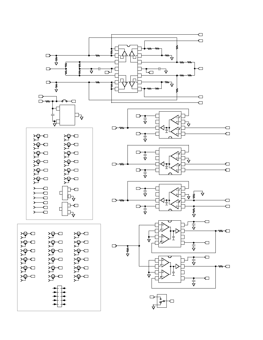
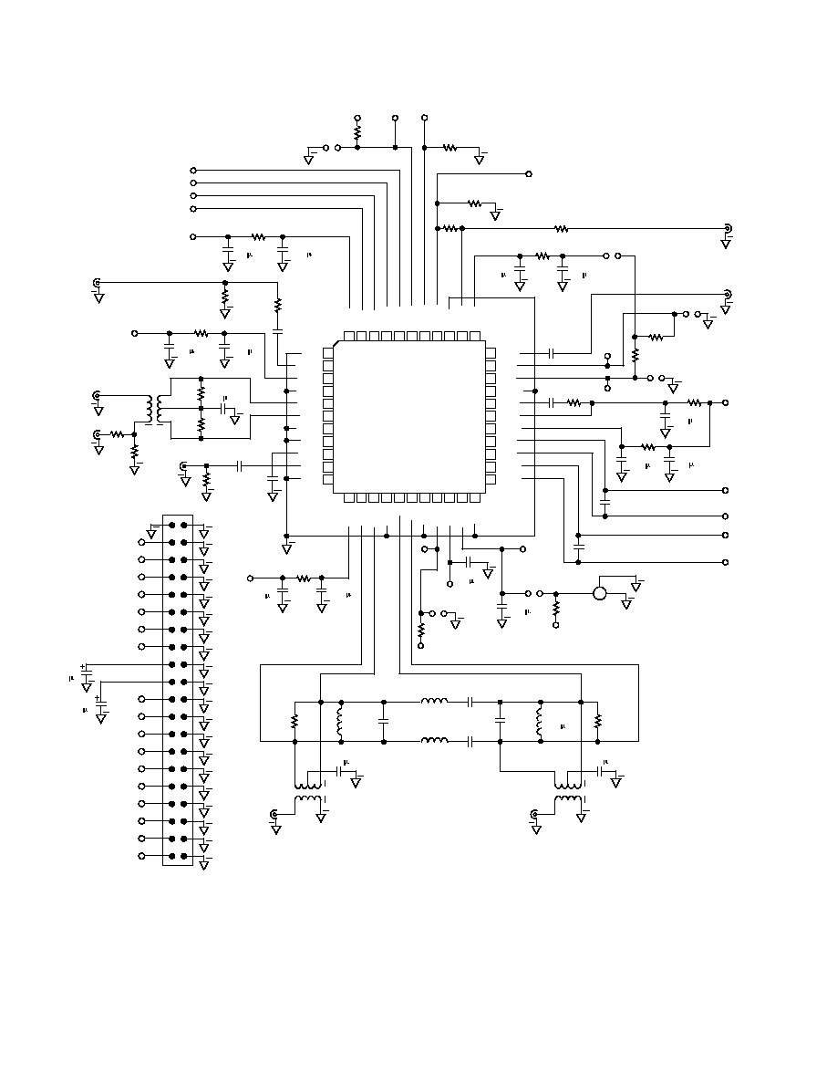
Figure 2. Characterization Test Set
AD6432
7
REV. 0
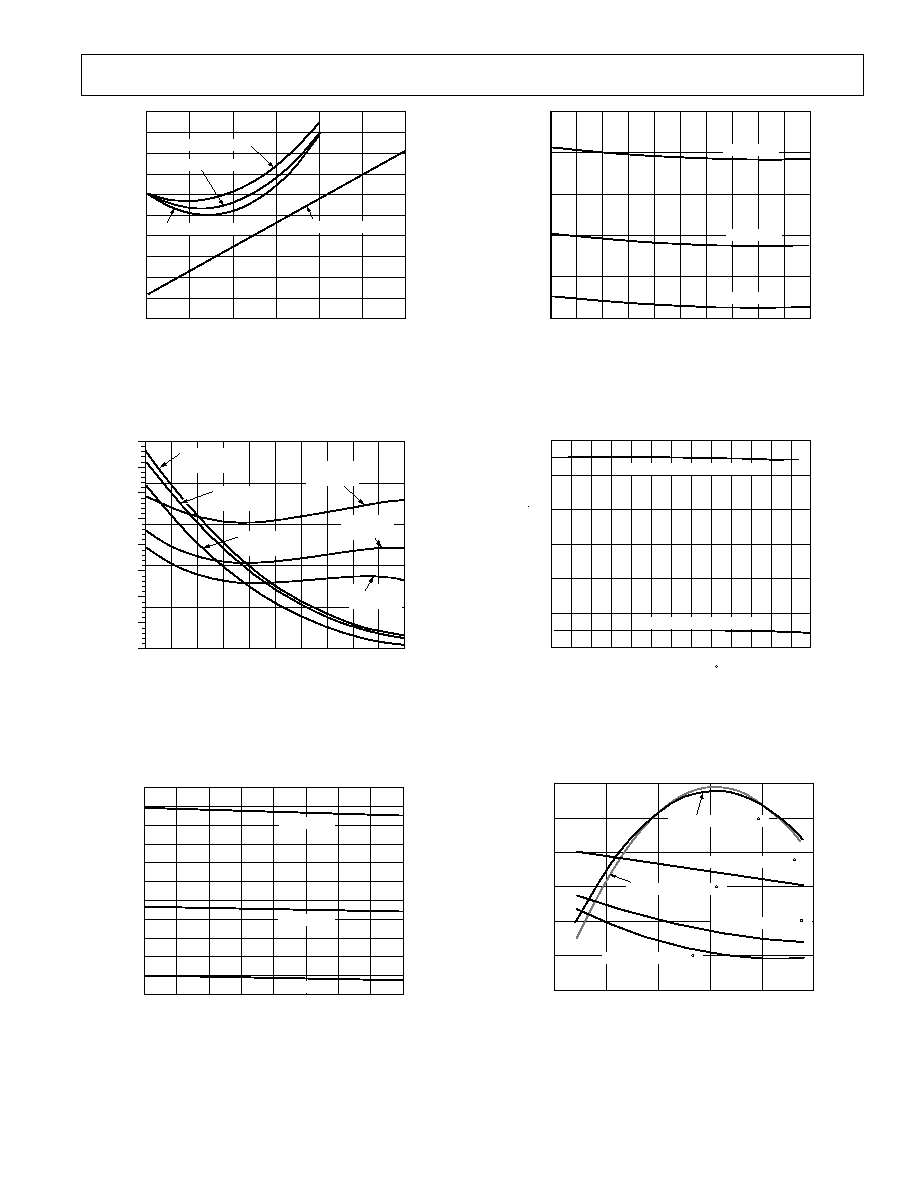
RF FREQUENCY MHz
SINGLE SIDEBAND Rx MIXER NOISE FIGURE dB
11
6
150
450
200
250
300
350
400
10.5
9
7.5
7
6.5
10
9.5
8.5
8
R
IN
= 50
, IF = 13MHz
R
IN
= 50
, IF = 45MHz
R
IN
= 50
, IF = 26MHz
R
IN
= 400
, IF = 13MHz
Figure 3. Rx Mixer Noise Figure vs. RF Frequency,
T
A
= +25
°
C, V
POS
= 3 V, V
GREF
= 1.2 V, V
GAIN
= 0.2 V
FREQUENCY MHz
900
800
50
550
100
150
200
250
300
350
400
450
500
700
600
500
400
SHUNT RESISTANCE
300
200
100
2.5
3.0
3.5
4.0
4.5
5.0
R
S
V
GAIN
= 2.4V
R
S
V
GAIN
= 1.2V
R
S
V
GAIN
= 0.2V
C
S
V
GAIN
= 2.4V
C
S
V
GAIN
= 1.2V
C
S
V
GAIN
= 0.2V
SHUNT CAPACITANCE pF
Figure 4. Rx Mixer Input Impedance vs. RF Frequency,
V
POS
= 3 V, T
A
= +25
°
C, V
GREF
= 1.2 V
RF FREQUENCY MHz
16
14
150
175
200
250
300
350
12
10
8
6
4
2
0
GAIN dB
2
4
6
225
275
325
V
GAIN
= 0.2V
V
GAIN
= 2.4V
V
GAIN
= 1.5V
Figure 5. Rx Mixer Conversion Gain vs. RF Frequency,
T
A
= +25
°
C, V
POS
= 3 V, V
GREF
= 1.2 V, F
IF
= 26 MHz
IF FREQUENCY MHz
20
15
10
14
18
26
34
42
10
5
0
GAIN dB
5
22
30
38
46
50
V
GAIN
= 1.5V
V
GAIN
= 0.2V
V
GAIN
= 2.4V
Figure 6. Mixer Conversion Gain vs. IF Frequency,
T
A
= +25
°
C, V
POS
= 3 V, V
GREF
= 1.2 V, F
RF
= 250 MHz
TEMPERATURE C
70
50
40 30 20
0
20
40
40
30
20
GAIN dB
10
10
10
30
50
60
AMP/DEMOD, V
POS
= 2.7V TO 3.6V
MIXER, V
POS
= 2.7V TO 3.6V
70
80
90
60
Figure 7. Rx Mixer Conversion Gain and IF Amplifier/
Demodulator Gain vs. Temperature, V
GAIN
= 0.2 V,
V
GREF
= 1.2 V, F
IF
= 26 MHz, F
RF
= 250 MHz
V
GAIN
Volts
12
0
13
14
15
16
V
POS
= 2.7V, T
A
= +85 C
10
V
POS
= 2.7V, T
A
= +25 C
V
POS
= 2.7V, T
A
= 25 C
V
POS
= 3.6V, T
A
= 40 C
V
POS
= 3.6V, T
A
= +85 C
0.5
1.0
1.5
2.0
2.5
11
INPUT dBm (REFERRED TO 50
)
Figure 8. Rx Mixer Input 1 dB Compression Point vs.
V
GAIN
, V
GREF
= 1.2 V, F
RF
= 250 MHz, F
IF
= 26 MHz
AD6432
8
REV. 0
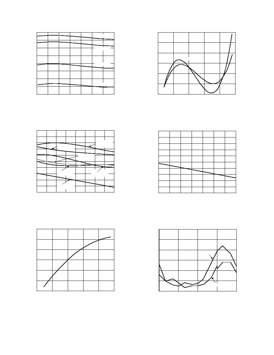
INTERMEDIATE FREQUENCY MHz
30
10
20
10
0
IF AMP/DEMOD GAIN dB
10
50
V
GAIN
= 0.2V
15
20
25
30
35
40
60
70
40
45
V
GAIN
= 0.5V
V
GAIN
= 1.5V
V
GAIN
= 2.4V
Figure 9. IF Amplifier and Demodulator Gain vs. IF
Frequency, T
A
= +25
°
C, V
POS
= 3 V, V
GREF
= 1.2 V
IF INPUT FREQUENCY MHz
10
15
20
25
30
35
13000
40
45
50
12000
11000
10000
9000
8000
7000
6000
5000
4000
3000
R
S
V
GAIN
= 2.4V
R
S
V
GAIN
= 1.2V
R
S
V
GAIN
= 0.2V
C
S
V
GAIN
= 0.2V
C
S
V
GAIN
= 1.2V
C
S
V
GAIN
= 2.4V
CAPACITANCE pF
2.0
RESISTANCE
2.2
2.4
2.6
2.8
3.0
3.2
3.4
3.6
3.8
4.0
Figure 10. IF Amplifier Input Impedance vs. Frequency,
T
A
= +25
°
C, V
POS
= 3 V, V
GREF
= 1.2 V
V
GAIN
Volts
0
0.5
1.0
1.5
2.0
2.5
60
50
40
30
20
10
0
IF INPUT 1dB COMPRESSION REFERRED
TO 50 OHMS dBm
Figure 11. IF Amplifier/Demodulator Input 1 dB
Compression Point vs. V
GAIN
, F
IF
= 26 MHz,
V
GREF
= 1.2 V, T
A
= +25
°
C, V
POS
= 3 V
V
GAIN
Volts
0
0.5
1.0
1.5
2.0
2.5
0.2
0.1
0
0.1
0.2
0.3
0.4
GAIN ERROR dB
MIXER
IF AMP/DEMOD
Figure 12. Gain Error vs. Gain Control Voltage, T
A
= +25
°
C,
V
POS
= 3 V, V
GREF
= 1.2 V, F
RF
= 250 MHz, F
IF
= 26 MHz
DEMODULATOR VCO FREQUENCY MHz
10
15
20
25
30
35
1.4
1.2
1.0
0.8
0.6
0.4
40
45
0.2
0
0.2
0.4
0.6
DEMODULATOR QUADRATURE ERROR Degrees
Figure 13. Demodulator Quadrature Error vs. FREF
Frequency, T
A
= +25
°
C, V
POS
= 3 V
FREQUENCY OFFSET kHz
0.1
1.0
10
100
1000
110
105
80
85
90
95
100
PHASE NOISE dBc/Hz
IF = 26MHz
IF = 13MHz
Figure 14. PLL Phase Noise vs. Frequency, V
POS
= 3 V,
C
FLTR
=1 nF, R
FLTR
=1 k
, FREF = 13 MHz
AD6432
9
REV. 0
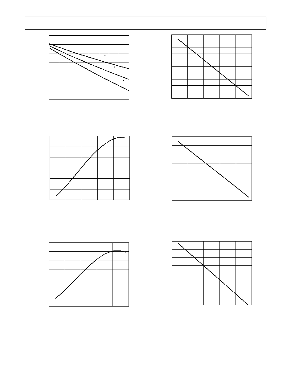
FREQUENCY OF VCO MHz
10
40
50
1.2
1.0
0
0.2
0.4
0.6
0.8
FILTER PIN VOLTAGE
REFERENCED TO V
POS
Volts
15
20
25
30
35
45
1.4
T
A
= 40 C
T
A
= +25 C
T
A
= +85 C
Figure 15. PLL Loop Voltage at FLTR Pin (KVCO) vs.
Frequency
GAIN VOLTAGE Volts
0
60
50
10
20
30
40
0.5
1.0
1.5
2.0
2.5
70
INPUT 1dB COMPRESSION POINT
REFERRED TO 50 OHMS dBm
Figure 16. System (Mixer + IF LC Filter + IF Amplifier +
Demodulator) 1 dB Compression Point vs. V
GAIN
, T
A
= +25
°
C,
V
POS
= 3 V, F
RF
= 250 MHz, F
IF
= 26 MHz, V
GREF
= 1.2 V
GAIN VOLTAGE Volts
0
60
50
10
20
30
40
0.5
1.0
1.5
2.0
2.5
70
0
SYSTEM INPUT IP3
REFERRED TO 50 OHMS dBm
Figure 17. System (Mixer + IF LC Filter + IF Amplifier +
Demodulator) IP3 vs. V
GAIN
, T
A
= +25
°
C, V
POS
= 3 V,
F
IF
= 26 MHz, F
RF
= 250 MHz, V
GREF
= 1.2 V
V
GAIN
Volts
0
4
6
14
12
10
8
0.5
1.0
1.5
2.0
2.5
2
16
CONVERSION GAIN dB
0
2
4
Figure 18. Rx Mixer Conversion Gain vs V
GAIN
, T
A
= +25
°
C,
V
POS
= 3 V, F
RF
= 250 MHz, F
IF
= 26 MHz, V
GREF
= 1.2 V
V
GAIN
Volts
0
40
50
70
60
0.5
1.0
1.5
2.0
2.5
30
20
IF AMP/DEMODULATOR GAIN dB
10
0
Figure 19. IF Amplifier/Demodulator Gain vs. V
GAIN
,
T
A
= +25
°
C, V
POS
= 3 V, F
RF
= 250 MHz, F
IF
= 26 MHz,
V
GREF
= 1.2 V
GAIN VOLTAGE Volts
0
40
50
70
60
0.5
1.0
1.5
2.0
2.5
30
20
10
0
80
SYSTEM GAIN dB
Figure 20. System (Mixer + IF LC Filter + IF Amplifier +
Demodulator) Gain vs. V
GAIN
, T
A
= +25
°
C, V
POS
= 3 V,
F
IF
=26 MHz, F
RF
= 250 MHz, V
GREF
= 1.2 V
AD6432
10
REV. 0
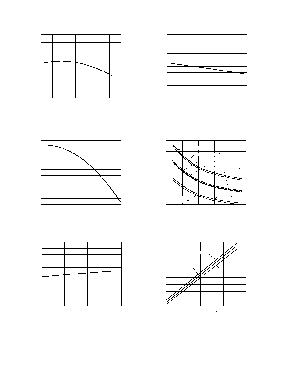
TEMPERATURE C
40
18.0
17.5
16.5
17.0
20
0
20
40
60
18.5
19.0
19.5
20.0
16.0
TRANSMIT DESIRED SIDEBAND GAIN dB
80
100
Figure 21. Tx Desired Sideband Gain vs. Temperature,
T
A
= +25
°
C, V
POS
= 3 V, F
CARRIER
= 280 MHz, I and Q Inputs
Driven in Quadrature
CARRIER FREQUENCY MHz
100
15.5
15.0
14.0
14.5
120
140
160
180
200
16.0
16.5
17.0
17.5
13.5
TRANSMIT DESIRED SIDEBAND GAIN dB
220
240
18.0
18.5
19.0
260
280
300
Figure 22. Tx Desired Sideband Gain vs. F
CARRIER
,
T
A
= +25
°
C, V
POS
= 3 V
TEMPERATURE C
40
37.0
36.5
35.5
36.0
20
0
20
40
60
37.5
38.0
38.5
39.0
35.0
80
100
39.5
40.0
TYPICAL UNDESIRED
SIDEBAND SUPPRESSION dBc
Figure 23. Tx Typical Undesired Sideband Suppression
vs. Temperature, T
A
= +25
°
C, V
POS
= 3 V
CARRIER FREQUENCY MHz
100
37.0
36.5
35.5
36.0
120
140
160
180
200
37.5
38.0
38.5
39.0
35.0
240
260
39.5
40.0
280
300
220
TYPICAL UNDESIRED
SIDEBAND SUPPRESSION dBc
Figure 24. Tx Typical Undesired Sideband Suppression
vs. F
CARRIER
, T
A
= +25
°
C, V
POS
= 3 V
GAIN VOLTAGE Volts
0
10
SUPPLY CURRENT mA
12
14
16
18
20
22
0.5
1.0
1.5
2.0
2.5
V
POS
= 3.6V, T
A
= +85 C
V
POS
= 2.7V, T
A
= +85 C
V
POS
= 3.6V, T
A
= +25 C
V
POS
= 3V, T
A
= +25 C
V
POS
= 2.7V, T
A
= +25 C
V
POS
= 3.6V
T
A
= 40 C
V
POS
= 2.7V
T
A
= 40 C
Figure 25. Rx Mode Supply Current vs. V
GAIN
, V
GREF
= 1.2 V
TEMPERATURE C
40
10.5
11.0
11.5
12.0
12.5
13.0
13.5
20
0
20
40
60
V
POS
= 3.6V
V
POS
= 3V
V
POS
= 2.7V
Tx MODE SUPPLY CURRENT mA
80
100
14.0
14.5
15.0
Figure 26. Tx Mode Supply Current vs. Temperature
AD6432
11
REV. 0
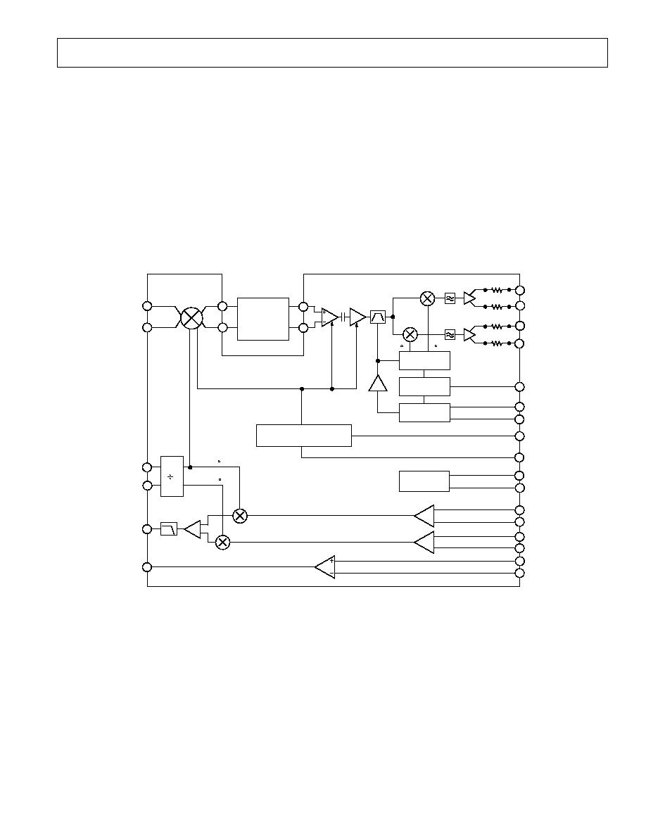
PRODUCT OVERVIEW
The AD6432 provides most of the active circuitry required to
realize a complete low power, single-conversion superhetero-
dyne time division transceiver, or the latter part of a double-
conversion transceiver, at input receive frequencies up to
350 MHz with an IF from 10 MHz to 50 MHz and transmit
frequencies up to 300 MHz. The internal I/Q demodulators,
with their associated phase-locked loop and the internal I/Q
modulator, support a wide variety of modulation modes, includ-
ing n-PSK, n-QAM, and GMSK. A single positive supply volt-
age of 3 V is required (2.7 V minimum, 3.6 V maximum) at a
typical supply current of 13 mA at midgain in receive mode and
13 mA in transmit mode. In the following discussion, V
POS
will
be used to denote the power supply voltage, which will be as-
sumed to be 3 V.
31
19
21
23
24
25
26
16
6
9
10
13
14
17
RFHI
RFLO
MXOP
MXOM
LC
BANDPASS
FILTER
IFIP
IFIM
90
0
3MHz
4.7k
4.7k
4.7k
4.7k
DIVIDE BY
1 OR 2
PHASE
DETECTOR
GAIN TEMP. COMPENSATION
33
29
20
39
42
43
40
41
38
37
LOHI
LOLO
MODO
PCAO
5
2
35
90
0
IRXN
IRXP
QRXN
QRXP
IFS0
FREF
FLTR
GAIN
GREF
RXPU
TXPU
ITXN
ITXP
QTXN
QTXP
PCAP
PCAM
QUADRATURE
VCO
RX, TX
BIAS
2
AD6432
Figure 27. Functional Block Diagram
Figure 27 shows the main sections of the AD6432. In the re-
ceive path, it consists of a variable-gain UHF mixer and linear
two-stage IF strip, both of which together provide a calibrated
voltage-controlled gain range of more than 80 dB, followed by a
tunable IF bandpass filter and dual quadrature demodulators.
These are driven by inphase and quadrature clocks generated
by a Phase-Locked Loop (PLL) locked to a corrected external
reference. In the transmit path it consists of a quadrature modu-
lator followed by a low-pass filter. The quadrature modulator is
driven by quadrature frequencies that are generated internally
by dividing the external local oscillator frequency by two. A
CMOS-compatible power-down interface completes the AD6432.
AD6432
12
REV. 0
Receive Mixer
The UHF mixer is an improved Gilbert-cell design that can
operate from low frequencies (it is internally dc-coupled) up to
an RF input of 350 MHz. The dynamic range at the input of the
mixer is determined, at the upper end, by the maximum input
signal level of
±
71 mV (13 dBm in 50
between RFHI and
RFLO) up to which the mixer remains linear and, at the lower
end, by the noise level. It is customary to define the linearity of
a mixer in terms of the 1 dB gain-compression point and third-
order intercept, which for the AD6432 are 13 dBm and 0 dBm,
respectively, in a 50
system.
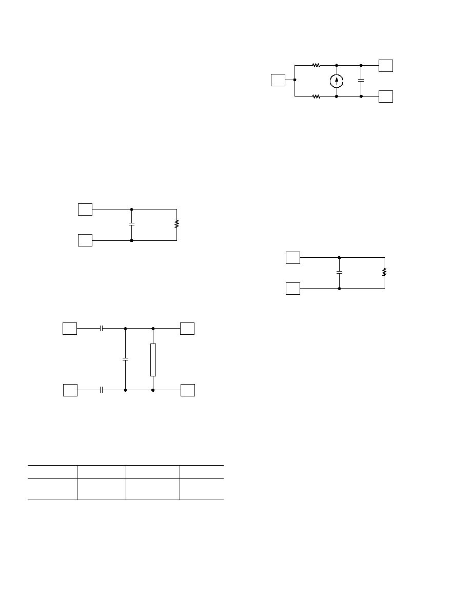
The mixer's RF input port is differential, that is, pin RFLO is
functionally identical to RFHI, and these nodes are internally
biased. The RF port can be modeled as a parallel RC circuit as
shown in Figure 29. The local oscillator input of the receive
mixer is internally provided by the LO divided by two.
RFHI
RFLO
C
SH
R
SH
Figure 28. Mixer Port Modeled as a Parallel RC Network
At V
GAIN
= 1.2 V and F
RF
= 250 MHz, C
SH
= 3.5 pF and
R
SH
= 400
(See Figure 4)
The output of the mixer is differential. The nominal conversion
gain is specified for operation into a 26 MHz LC IF bandpass
filter, as shown in Figure 29 and Table I.
MXOP
C1
C2
C1
L1
MXOM
IFIM
IFIP
Figure 29. Suggested IF Filter Inserted Between the
Mixer's Output Port and the Amplifier's Input Port
The conversion gain is measured between the mixer input and
the input of this filter, and varies between 3 dB and +15 dB.
Table I. Filter Component Values for Selected Frequencies
Frequency
C1
L1
C2
13 MHz
27 pF
0.82
µ
H
180 pF
26 MHz
22 pF
0.39
µ
H
82 pF
The maximum permissible signal level between MXOP and
MXOM is determined by the maximum gain control voltage.
The mixer output port, having pull-up resistors of 250
to
VPRX, is shown in Figure 30.
VPRX
MXOP
250
250
MXOM
Figure 30. Mixer Output Port
IF Amplifier
Most of the gain in the AD6432 receive section is provided by
the IF amplifier strip, which comprises two stages. Both are fully
differential and each has a gain span of 31 dB for the AGC volt-
age range of 0.2 V to 2.4 V. Thus, in conjunction with the vari-
able gain of the mixer, the total gain span is 80 dB. The overall IF
gain varies from 14 dB to +48 dB for the nominal AGC voltage of
0.2 V to 2.4 V. Maximum gain is at V
GAIN
= 0.2 V.
The IF input is differential, at IFHI and IFLO. Figure 32 shows
a simplified schematic of the IF interface modeled as parallel
RC network.
The operative range of the IF amplifier is approximately 50 MHz
from IFHI and IFLO through the demodulator.
IFHI
IFLO
C
SH
R
SH
Figure 31. IF Amplifier Port Modeled as a Parallel RC
Network for V
GAIN
= 1.2 V and F
IF
= 26 MHz, C
SH
= 3 pF,
R
SH
= 8.5 k
(See Figure 10)
Gain Scaling
The overall gain of the AD6432, expressed in decibels, is linear
with respect to the AGC voltage V
GAIN
at Pin GAIN. The gain
of all sections is maximum when V
GAIN
is 0.2, and falls off as the
bias is increased to V
GAIN
= 2.4 V and is independent of the
power supply voltage. The gain of all stages changes simulta-
neously. The AD6432's gain scaling is also temperature-
compensated. Note that GAIN pin of the AD6432 is an input
driven by an external low impedance voltage source, normally a
DAC, under the control of radio's digital processor.
The gain-control scaling is directly proportional to the reference
voltage applied to the Pin GREF and is independent of the
power supply voltage. When this input is set to the nominal
value of 1.2 V, the scale is nominally 27.5 mV/dB (36.4 dB/V).
Under these conditions, 80 dB of gain range (mixer plus IF)
corresponds to a control voltage of 0.2 V < = V
G
< = 2.4 V. The
final centering of this 2.2 V range depends on the insertion losses of
the IF filters used.
Pin GREF can be tied to an external voltage reference, V
REF
,
provided, for example, by a AD1580 (1.21 V) voltage reference.
When using the Analog Devices AD7013 (IS54, TETRA and
satellite receiver applications) and AD7015 or AD6421 (GSM,
DCS1800, PCS1900) baseband converters, the external refer-
ence may also be provided by the reference output of the
AD6432
13
REV. 0
baseband converters. The interface between the AD6432 and
the AD6421 baseband converter is shown in Figure 35. The
AD7015 baseband converter provides a V
R
of 1.23 V; an auxil-
iary DAC in the AD7015 can be used to generate the AGC
voltage. Since it uses the same reference voltage, the numerical
input to this DAC provides an accurate RSSI value in digital
form, no longer requiring the reference voltage to have high
absolute accuracy.
Tunable Filter and I/Q Demodulators
The demodulators (I and Q) receive their inputs internally from
the IF amplifier through a two-pole tunable-frequency bandpass
filter. This filter is centered on the IF frequency and its band-
width is approximately equal to forty per cent of the IF fre-
quency. The filter attenuates the amount of noise present at the
input of the demodulators.
Each demodulator comprises a full-wave synchronous detector
followed by a 3 MHz, two-pole low-pass filter, producing differ-
ential outputs at pins IRXP and IRXN, and QRXP and QRXN.
Using the I and Q demodulators for IFs above 50 MHz is pre-
cluded by the 10 MHz to 50 MHz range of the PLL used in the
Demodulator section.
The I and Q outputs are differential and can swing up to 2 V p-p
at the low supply voltage of 2.7 V. They are nominally centered
at 1.5 V independent of power supply. They can therefore
directly drive the receive ADCs in the AD7015 or AD6421
baseband converters, which require an amplitude of 1.23 V to
fully load them when driven by a differential signal. The conver-
sion gain of the I and Q demodulators is 17 dB.
A simple 1-pole RC filter at the I and Q outputs, with its corner
above the modulation bandwidth is sufficient to attenuate un-
desired outputs. The design of the RC filter is eased by the
4.7 k
resistor integrated into each I and Q output pin.
Phase-Locked Loop
The demodulators are driven by quadrature signals that are
provided by a variable-frequency quadrature oscillator (VFQO),
phase-locked to the reference frequency. This frequency is equal
or double the frequency of the signal applied to Pin FREF.
When the quadrature signals are at the IF, inphase and quadra-
ture baseband outputs are generated at the I output (IRXP
and IRXN) and Q output (QRXP and QRXN), respectively.
The quadrature accuracy of the VFQO is typically within
±
1
°
at
26 MHz. A simplified diagram of the FREF input is shown in
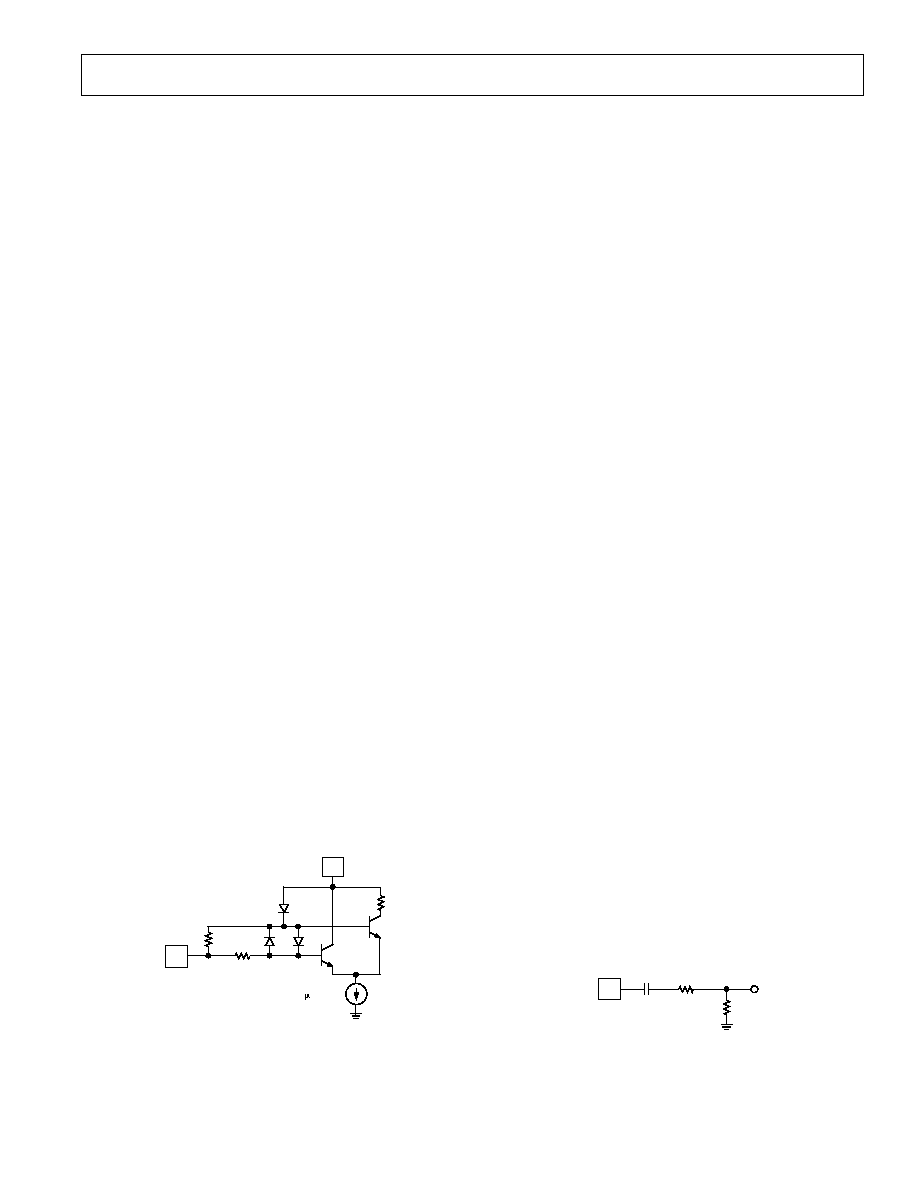
Figure 32.
VPOS
5k
20k
5k
FREF
50 A PTAT
Figure 32. Simplified Schematic of the FREF Interface
The VFQO is controlled by the voltage between V
POS
and
FLTR. In normal operation, a series RC network, forming the
PLL loop filter, is connected from FLTR to V
POS
. The use of an
integral sample-hold system ensures that the frequency-
control voltage on Pin FLTR remains held during power-
down, so reacquisition of the carrier occurs in less than
80
µ
s.
In practice, the probability of a phase mismatch at power-
up is high, so the worst-case linear settling period to full
lock needs to be considered in making filter choices. This
is typically < 80
µ
s for a locking error of
±
3
°
at an IF of
26 MHz. Note that the VFQO always provides quadrature
between its own I and Q outputs, but the phasing between
it and the reference carrier will swing around the final value
during the PLL's settling time.
I and Q Transmit Modulator
The transmit modulator uses two standard mixer cells
whose linear inputs are the differential voltages at the input
Pins ITXP/ITXN and QTXP/QTXN, respectively and whose
local oscillator inputs are derived from a divide-by-two cell,
driven from the input applied to pins LOHI/LOLO. The
outputs of the mixers are summed and converted to single-
sided form. The output stage also filters the higher harmon-
ics, minimizing the need for filtering before this signal is
presented to the up-converter in a typical transmitter
configuration.
The I and Q inputs are intended to be driven using a
fully-differential drive (for example from an AD7015 or
AD6421) and need to be biased to a common-mode dc
level of 1.2 V, with a typical differential amplitude of
±
1.028 V (that is,
±
514 mV at each input). Some small
variation in the drive conditions is allowable, but will result
in nonoptimal performance. The minimum instantaneous
input should not go below 0.6 V and the maximum voltage
should not exceed 1.8 V using a 2.7 V supply (in general,
VP 0.9 V). The impedance at these inputs is several M
in parallel with approximately 1 pF; the bias currents flow
out of the pins and are ~100 nA. These conditions permit
the use of a high impedance low-pass filter if desired ahead
of the modulator inputs.
The dc modulator output is at a constant dc level of 1.5 V,
independent of temperature and supply voltage. It is de-
signed to drive a 150
load and should either be matched
into a 50
load, using a simple LC network, or padded to
150
with a series 100
resistor (Figure 33). The output
is short-circuit-proof. The output modulated signal at pin
MODO has a power of 16 dBm when driving a 50
load
with a 100
series resistor, as shown in Figure 33. This
power is specified at a carrier frequency of 272 MHz with a
maximum dc differential signal applied to the I or Q chan-
nel while the other channel has no differential signal ap-
plied. The transmit modulator is enabled only when the
TXPU input (Pin 39) is taken HI.
50
100
MODO
100pF
Figure 33. Output Impedance of Pin MODO Is
Designed to Drive a 50
Load with a 100
Series
Resistor
AD6432
14
REV. 0
Local Oscillator Input
The Local Oscillator (LO) input port is differential and consists
of two functionally identical pins, LOHI and LOLO. It accepts
a signal of 200 mV p-p at a frequency between 200 MHz and
600 MHz. Inputs LOHI and LOLO are internally biased to the
positive supply (Pin 3) through 500
resistors. While not usu-
ally needed, these inputs may be driven through a simple match-
ing network to lower the LO power required from a 50
source.
Single-sided drives are not recommended. The most noticeable
effects will be degradation of phase balance and an increase in
phase noise.
This signal is fed internally to a divider by two that generates the
mixing signals for the receive mixer and the transmit modulator.
In order to meet the phase and amplitude balance of the trans-
mit quadrature modulator, as stated in the specification table,
the duty cycle of the LO signal must be such that the second
harmonic is at least 30 dBc below the fundamental.
I/Q Convention
The AD6432 is a complete IF subsystem. Although not a re-
quirement for using the AD6432, most applications will use a
high side LO injection on the receive mixer. The I and Q con-
vention on the receive section is such that when a spectrum with
I leading Q is presented to the input of the receive mixer and a
high side LO is presented to the receive mixer, I still leads Q at
the baseband output of the AD6432.
Likewise, the I and Q convention on the transmit section is
such that when a spectrum with I leading Q is presented at the
baseband input of the modulator, I still leads Q at the output of
the modulator.
Auxiliary Op Amp
An auxiliary operational amplifier is available although it is im-
portant to remember that it is active only when TXPU is high.
The positive and negative input terminals are PCAP and PCAM
with PCAO being the output pin. The inputs are the bases of
PNP transistors with a typical bias current of approximately
150 nA. The input offset voltage is typically < 4 mV and the
open loop gain of the amplifier is 60 dB. The amplifier is unity
gain stable with a 3 dB Bandwidth greater than 40 MHz. The
input signal voltage range is from 0.1 V to V
POS
2.1 V.
Bias System
The AD6432 operates from a single supply, V
POS
, usually 3 V, at
a typical supply current in receive mode of 13 mA at midgain
and T
A
= +25
°
C, corresponding to a power consumption of
39 mW. Any voltage from 2.7 V to 3.6 V may be used.
The bias system includes a fast-acting active high CMOS-com-
patible power-up switch, allowing the part to idle at less than
100
µ
A when disabled. Biasing is generally proportional-to-
absolute temperature (PTAT) to ensure stable gain with tem-
perature. Other special biasing techniques are used to ensure
very accurate gain, stable over the full temperature range.
USING THE AD6432
In this section, we will focus on a few areas of special impor-
tance through the real life example of interfacing the AD6432
to the AD6421 Base Band converter. As is true of any wideband
high gain components, great care is needed in PC board layout.
The location of the particular grounding points must be considered
with due regard for the possibility of unwanted signal coupling.
The high sensitivity of the AD6432 leads to the possibility
that unwanted local EM signals may have an effect on the per-
formance. During system development, carefully-shielded test
assemblies should be used. The best solution is to use a fully
enclosed box enclosing all components, with the minimum
number of needed signal connectors (RF, LO, I and Q outputs)
in miniature coax form.
Interfacing the AD6432 to the AD6421 Baseband Converter
The AD6421 Baseband Converter contains all the necessary
elements to drive the AD6432.
Receive Interface
The interface between the two devices provides for quadrature
I and Q channels that can be driven either differentially or in the
single-ended configuration. Figure 35 shows the interface be-
tween the AD6432 and the AD6421 for the differential configu-
ration. The respective pins (IRXP, IRXN, QRXP and QRXN)
are dc coupled through 4.7 k
resistors, which are integrated
within the AD6432. Balanced coupling may be used with a
single 50 pF capacitor between the complementary signals as
illustrated in Figure 35. This low-pass filter is the only external
filter required to prevent aliasing of the baseband analog signal
prior to sampling within the AD6421.
The AD6421 has an external autocalibration mode that can
calibrate out any offsets resulting from the IF demodulation
circuitry.
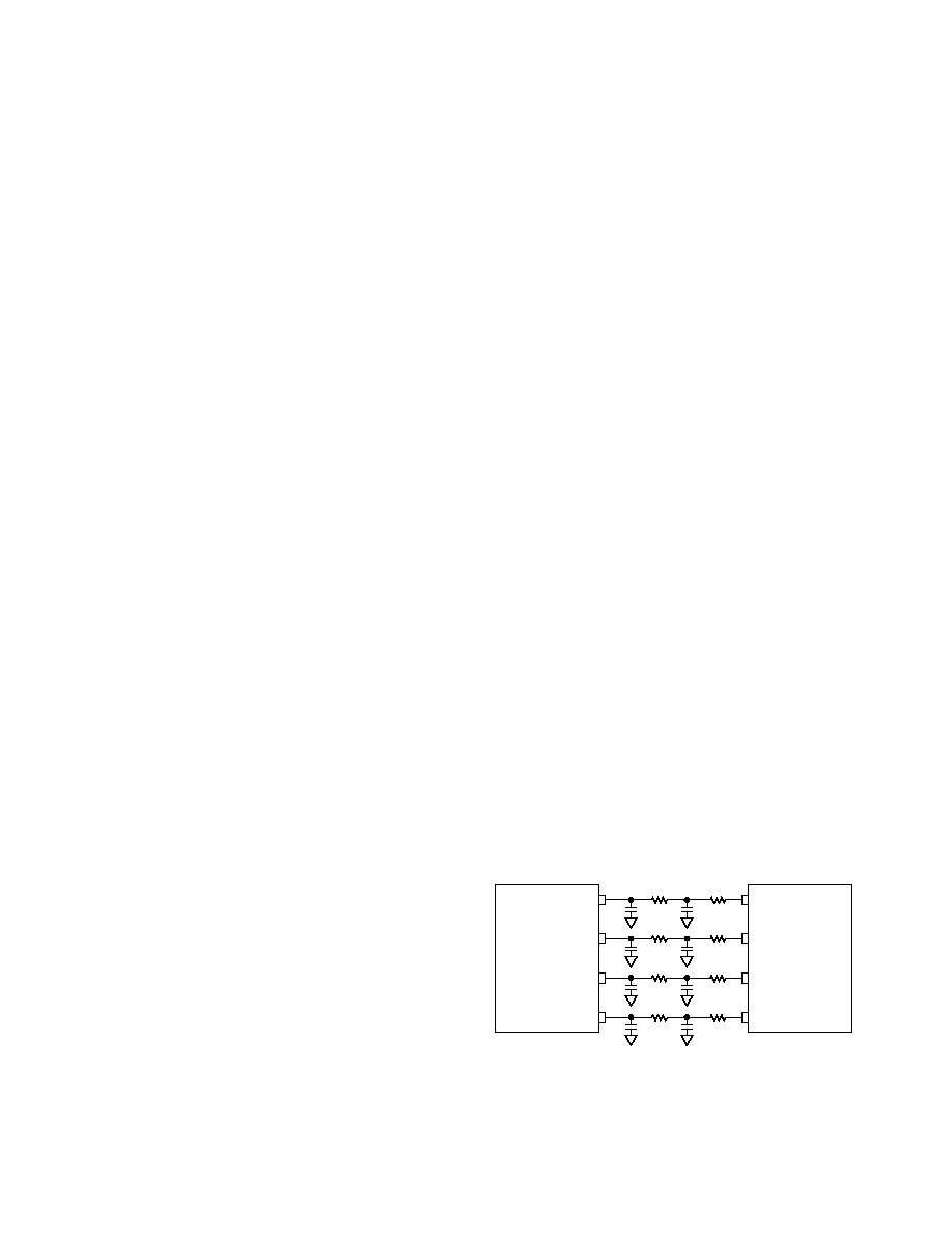
Transmit Interface
The corresponding transmit (ITXP, ITXN, QTXP and QTXN)
pins of the AD6421 and AD6432 are directly connected as these
have compatible bias levels for dc coupling. To meet the more
stringent phase two filter mask requirements, an external low-
pass filter may be required, depending on the filtering capabili-
ties of the radio section. A passive second order low-pass
filter network with a cutoff frequency to 600 kHz is suggested
as shown in Figure 34. Resistor values should range from
1.5 k
3.0 k
to minimize AD6432 offsets.
QTXN
QTXP
ITXN
ITXP
AD6432
AD6421
ITXP
ITXN
QTXP
QTXN
Figure 34. GSM Phase II Transmit Interface
AD6432
15
REV. 0
Gain Control
The AD6432 contains a Gain TC Compensation circuit that
provides a nominal 80 dB dynamic range of automatic gain
control. The GAIN input pin of the gain circuit is driven by
the AD6421 Automatic Gain Control DAC (AGCDAC), an
integrated auxiliary DAC of the AD6421, controllable by the
radio's digital processor. This connection should be made
through a single pole RC to reduce high frequency noise into
the gain control circuit. The values shown in Figure 35 provide
a 3 dB point at approximately 1 MHz, sufficient for the gain
control.
Gain control scaling is directly proportional to the reference
voltage applied to Pin GREF and is independent of the power
supply voltage. A nominal 1.2 V reference for GREF can be
provided by the AD6421 through BREFOUT. BREFOUT is
a buffered output version of BREFCAP reference. This refer-
ence output feature is enabled on the AD6421 by setting Bit 2
in control register BCRB (BCRB2). See AD6421 data sheet.
The V
GAIN
input range for this control signal is 0.2 V 2.4 V where
gain is maximum at 0.2 V and falls off as V
GAIN
is increased to
2.4 V. To avoid saturating the input to the baseband converter,
the automatic gain control function of the receiver must limit
the output signal swing of the AD6432 to
±
1.2 V, the full signal
range of the input.
Phase-Lock Loop Control
The AD6432 PLL/QVCO circuits require an external frequency
reference for coherent modulation and demodulation of the
baseband and IF signal. The external frequency reference con-
trol for the AD6432 PLL/QVCOs is typically generated through
a 13 MHz voltage controlled temperature compensated crystal
oscillator (VCTCXO). The control voltage for the VCTCXO is
generated by an auxiliary DAC in the AD6421 designated as
the Automatic Frequency Control DAC (AFCDAC). The PLL
loop is closed through the radio's algorithm signal processor,
which drives the AD6421 AFCDAC.
The AD6432 FREF pin provides the VCTCXO reference sig-
nal to the AD6432 RX quadrature VCO (QVCO) circuit.
The AD6432 FREF input must be an ac coupled signal
200 mV p-p or greater. The reference for the UHF TX QVCO
and RX IF down converter is synthesized from the VCTCXO
output reference signal through an external frequency synthe-
sizer and VCO. This UHF reference is an ac coupled input into
AD6432 LOHI and LOLO pins.
An external series RC network connected between FLTR (Pin
29) and the VPOS supply pin provides the proper loop filter for
the VCO/PLL as shown in Figure 35.
LC
BAND-
PASS
FILTER
FREQUENCY
SYNTHESIZER
VCTCXO
50pF
1k
100nF
0.1 F
160
1nF
1nF
ITXP
ITXN
QTXP
QTXN
AD6421
IRXP
IRXN
QRXP
QRXN
AFCDAC
MCLK
BREFCAP
BREFOUT
AGCDAC
RAMDAC
POWER CONTROL
50pF
GAIN
GREF
LOLO
LOHI
FREF
QRXN
QRXP
IRXN
IRXP
QTXN
QTXP
ITXN
ITXP
IFHI
IFLO
MXLO
MXHI
AD6432
Figure 35. AD6432 to AD6421 Interface
Transmit Power Control
A general purpose amplifier is available on the AD6432, which
may be useful as part of an automatic control circuit for the
power amplifier. Open ended, this amplifier will swing full scale
from rail to rail. It is recommended that this amplifier be con-
nected in the unity feedback configuration when not being used
by connecting PCAO to PCAM.
AD6432 EVALUATION BOARD
The AD6432 Evaluation Board is designed to enable measure-
ments of key parameters on the AD6432 IFIC, a device that
provides the complete transmit and receive IF signal processing,
including I/Q modulation and demodulation, necessary to imple-
ment a digital wireless transceiver.
Many of the signal paths into and out of the AD6432 are differ-
ential, which is the preferred interface to and from single supply
CODECS. To facilitate an interface to traditional lab equip-
ment, the following interface circuitry is included on the board.
A 20-pin Berg strip for bias, gain and Inphase and Quadrature
signal interface. End Launch SMA connectors for RF, LO,
MODO and FREF signals and provisions for breaking out
MXOP and IFHI with RF transformers.
A single-ended to differential RF transformer provides a bal-
anced LO drive.
An onboard 1.2 V dc reference IC is provided for application to
GREF.
AD6432
16
REV. 0
Evaluation Board Description
This four layer board demonstrates both the transmit and
receive functions of the AD6432. The top internal layer is a
ground plane and the bottom internal layer is a strategically
partitioned power plane with DUT power and bipolar support
device power.
A 20-pin Berg strip connector provides the external power and
dc signal interface, which includes power-up, gain and external
reference bias options. The various high frequency IF, LO, TX
Modulation output (MODO) and the Demodulator Reference
(FREF) are brought in and out of the board via end-launch
SMA connectors. Appropriate terminations are provided for
each signal. Several hardware jumpers are provided for bias and
IF selection options. Figure 36 shows the placement of the
different connectors used on the evaluation board.
FREF
MODO
LOINP
OPTLO
RFHI
T1
U1
Q1
J23
J25
J24
J26
J21
INTERFACE CONNECTOR
1
AD6432 EVAL.
REV. B
MXOP
IFIP
J22
Figure 36. Evaluation Board Layout (Top View)
Note: MXOP, IFHI, OPTLO are optional SMA connectors not
supplied with the evaluation board.
Interface Connector (Berg Strip) Pin Description
Building up a simple IDC connector/ribbon cable breakout to a
vector board or box with banana plugs will facilitate testing.
Figure 37 shows the signal's placement and Table II describes
each signal.
BOARD
EDGE
GND
ITXP
ITXN
QTXP
PCAM
PCAP
VS2
VS1
PCAO
IFS0
IRXP
IRXN
QRXP
QRXN
GREF
GAIN
QTXN
TXPU
RXPU
GND
Figure 37. Evaluation Board Interface Connector

AD6432
17
REV. 0
Table II. Connector Signal Description
Pin
Name
Description
GND
Analog and Power Ground.
ITXP
I Channel Transmit Plus Modulation Input.
ITXN
I Channel Transmit Minus Modulation Input.
QTXP
Q Channel Transmit Plus Modulation Input.
QTXN
Q Channel Transmit Minus Input.
TXPU
Transmit Section Power-Up. This function is
also jumper selectable with J21.
PCAM
Auxiliary Op Amp Minus Input.
PCAP
Auxiliary Op Amp Plus Input.
VS2
Power control op amp supply 2.7 V dc3.6 V dc.
The jumper, J26, connects VS1 and VS2 together.
VS1
AD6432 main supply 2.7 V dc3.6 V dc.
PCAO
Auxiliary Op Amp Output.
IFS0
Selects IF Pin. This function is also jumper pro-
grammable with J25.
IRXP
I Channel Receive Plus Modulation Output.
IRXN
I Channel Receive Minus Modulation Output.
QRXP
Q Channel Receive Plus Modulation Output.
QRXN
Q Channel Receive Plus Modulation Output.
GREF
The AD6432 gain reference bias which is optimized
for 1.2 V dc. This may be externally supplied; or by
shorting J23, supplied directly from the AD1580
SOT-23 onboard, 1.2 V reference.
GAIN
Max RX gain occurs at 0.2 V dc. Minimum gain
occurs at 2.4 V dc.
RXPU
Receive Section Power-Up. This function is also
jumper selectable with J22.
Power Requirements
The evaluation board uses two supplies, VS1 and VS2.
VS1--2.7 V dc3.6 V dc, 13 mA typical. This is the main sup-
ply for the AD6432.
VS2--2.7 V dc3.6 V dc, 2 mA typical. This is the supply for
the on-chip op amp which is normally used in RF power control
circuits.
The op amp is active only in the Transmit mode.
Table III. SMA End-Launch Connectors
SMA
Connector Description
MODO
Transmit Modulator Output. This pin, which is
designed to drive a 150
filter, has been resistively
matched (loss) onboard to drive a 50
instrument
such as a spectrum analyzer.
LOIP
Local Oscillator Input pin. This is actually fed with
twice the LO frequency from a generator for both
transmit and receive. The nominal LO level is
16 dBm (50
).
OPTLO
Optional differential minus local oscillator input
(transformer can be removed).
RFHI
RF input
MXOP
Mixer Output (optional output that may be converted
to single ended output with an RF transformer).
IFHI
IF Input (optional single ended input that may be
converted to differential with an RF transformer).
FREF
Frequency Reference for phase locked receive de-
modulator. The internal VCO frequency is equal to
FREF in the 1X mode and equal to two times FREF
in the 2X mode.
AD6432
18
REV. 0
4
6
1
2
3
4
6
1
2
3
MXOP
R6
OPEN
C18
OPEN
L1
OPEN
L2
SHORT
L3
SHORT
C16
22pF
C19
22pF
C20
82pF
L4
0.39 H
R13
OPEN
T2
C42
0.01 F
R3
49.9
C1
100pF
R9
84
MODO
R25
1k
C29
0.1 F
R34
0
C11
0.01 F
C10
1nF
C32
0.1 F
VS2
VPDV
DECOUPLING
VS1
R2
0
R23
123
QTXN
QTXP
ITXN
PCAP
R30
1k
C5
0.01 F
R12
0
R1
1k
R14
125
R8
0
IFS1
IFS0
C36
1nF
R6
0
C41
0.01 F
C17
0.1 F
C23
0.01 F
R7
0
C6
47pF
C8
47pF
IRXP
IRXN
QRXP
QXRN
C28
0.1 F
VPTX
DECOUPLING
C14
0.01 F
C15
100pF
LOIP
ITXP
VS1
RFHI
C2
100pF
R31
0
VS1
C30
0.1 F
C3
0.01 F
RXPU
GAIN
GREF
PCAO
FREF
VS1
C21
0.1 F
J22
VS1
C44
0.01 F
TP1580
R16
10k
Q1
J23
VS1
R35
125
OPTLO
R20
OPEN
TXPU
PCAM
R39
OPEN
VS1
R19
20k
J21
VS1
J26
R17
20k
R18
20k
ITXP
ITXN
QTXP
QTXP
TXPU
PCAM
PCAP
PCAO
IFS0
GND
IRXP
IRXN
QRXP
QRXN
GREF
GAIN
RXPU
GND
C50
4.7 F
C12
4.7 F
TX
20A 20B
VS2
VS1
J24
J25
29
30
31
32
33
27
28
25
26
23
24
40 39 38
41
42
43
44
36 35 34
37
12 13
14 15 16 17 18 19 20 21 22
3
4
5
6
7
1
2
10
11
8
9
VPDV
MODO
GND
CMTX
LOLO
LOHI
CMRX
GND
RFLO
RFHI
GND
FREF
GND
IFS0
CMDM
FLTR
VPFL
VPDM
IRXP
IRXN
QRXP
QRXN
VPTX
ITXP
ITXN
QTXP
QTXN
TXPU
PCAP
PCAM
GND
VPRX
MXHI
MXLO
IFLO
IFHI
VPPC
CMIF
CMIF
RXPU
GAIN
GREF
GND
AD6432
TOP VIEW
(Pins Down)
PCAO
R21
0
C18
0.1 F
1
2
3
4
6
T1
R15
20k
IFIP
T3
C43
0.01 F
Figure 38. Evaluation Board Schematics
AD6432
19
REV. 0
OUTLINE DIMENSIONS
Dimensions shown in inches and (mm).
44-Lead Plastic Thin Quad Flatpack (TQFP)
(ST-44)
TOP VIEW
(PINS DOWN)
1
33
34
44
11
12
23
22
0.018 (0.45)
0.012 (0.30)
0.031 (0.80)
BSC
0.394
(10.0)
SQ
0.472 (12.00) SQ
0.057 (1.45)
0.053 (1.35)
0.006 (0.15)
0.002 (0.05)
SEATING
PLANE
0.063 (1.60)
MAX
0.030 (0.75)
0.018 (0.45)

20
C3061124/97
PRINTED IN U.S.A.