 | ÐлекÑÑоннÑй компоненÑ: AD6459ARS | СкаÑаÑÑ:  PDF PDF  ZIP ZIP |
Äîêóìåíòàöèÿ è îïèñàíèÿ www.docs.chipfind.ru
REV. 0
Information furnished by Analog Devices is believed to be accurate and
reliable. However, no responsibility is assumed by Analog Devices for its
use, nor for any infringements of patents or other rights of third parties
which may result from its use. No license is granted by implication or
otherwise under any patent or patent rights of Analog Devices.
a
AD6459
One Technology Way, P.O. Box 9106, Norwood, MA 02062-9106, U.S.A.
Tel: 617/329-4700
World Wide Web Site: http://www.analog.com
Fax: 617/326-8703
© Analog Devices, Inc., 1996
GSM 3 V Receiver IF Subsystem
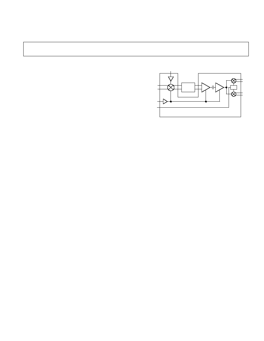
FUNCTIONAL BLOCK DIAGRAM
BPF
PLL
LO
I
Q
GAIN
CONTROL
FREF
RF
AD6459
FEATURES
Fully Compliant with Standard and Enhanced GSM
Specification
11 dBm Input 1 dB Compression Point
0 dBm Input Third Order Intercept
10 dB SSB Noise Figure (50 )
DC-500 MHz RF and LO Bandwidths
Linear IF Amplifier
Linear-in-dB and Stable over Temperature
Voltage Gain Control
Quadrature Demodulator
On-Board Phase-Locked Quadrature Oscillator
Demodulates IFs from 5 MHz to 50 MHz
Low Power
8 mA at Midgain
2 A Sleep Mode Operation
2.7 V to 5.5 V Operation
Interfaces to AD7013, AD7015 and AD6421 Baseband
Converters
20-Lead SSOP
GENERAL DESCRIPTION
The AD6459 is a 3 V, low power receiver IF subsystem for
operation at input frequencies as high as 500 MHz and IFs
from 5 MHz up to 50 MHz. It is optimized for operation in
GSM, DCS1800 and PCS1900 receivers. It consists of a mixer,
an IF amplifier, I and Q demodulators, a phase-locked quadra-
ture oscillator, a precise AGC subsystem, and a biasing system
with external power-down.
The AD6459's low noise, high intercept mixer is a doubly-
balanced Gilbert-Cell type. It has a nominal 11 dBm input-
referred 1 dB compression point and a 0 dBm input-referred
third-order intercept. The mixer section of the AD6459 also
includes a local oscillator (LO) preamplifier, which lowers the
required LO drive to 16 dBm.
The gain control input accepts an external gain-control voltage
input from an external AGC detector or a DAC. It provides an
80 dB gain range with 27 mV/dB gain scaling.
The I and Q demodulators provide in-phase and quadrature
baseband outputs to interface with Analog Devices' AD7013
(IS54, TETRA, MSAT) AD7015 and AD6421 (GSM,
DCS1800, PCS1900) baseband converters. An on-board
quadrature VCO that is externally phase-locked to the IF signal
drives the I and Q demodulators. This locked reference signal is
normally provided by an external VCTCXO under the control of
the radio's digital processor. The AD6459 can also provide
demodulation of N-PSK and N-QAM in many non-TDMA
systems when used with external analog carrier recovery systems
such as the Costas Loop. Finally, the VCO can be phase-locked
to a frequency that is deliberately offset from the IF as in the
case of a Beat-Frequency oscillator (BFO) resulting in the
product detection of CW or SSB.
The AD6459 uses supply voltages from 2.7 V to 5.5 V over the
temperature range of 40
°
C to +85
°
C. Operation is enabled by a
CMOS logical level; response time is typically < 80
µ
s. When
disabled, the standby current is reduced to 2
µ
A.
The AD6459 comes in a 20-pin shrink small outline (SSOP)
surface mount package.

2
REV. 0
AD6459SPECIFICATIONS
Model
AD6459ARS
Parameter
Conditions
Min
Typ
Max
Units
DYNAMIC PERFORMANCE
MIXER
Maximum RF and LO Frequency
500
MHz
AGC Conversion Gain Variation
0.2 V < V
GAIN
< 2.25 V
3 to +16
dB
Input 1 dB Compression Point
@ V
GAIN
= 0.2 V
11
dBm
Input Third-Order Intercept
@ V
GAIN
= 0.2 V
0
dBm
SSB Noise Figure
1
@ Z
S
= 50
, F
RF
= 240 MHz, F
LO
= 229.3 MHz at 16 dBm
10
dB
Mixer Output Bandwidth at MXOP
@ 3 dB
80
MHz
IF AMPLIFIERS
AGC Gain Variation
0.2 V < V
GAIN
<2.25 V
13 to +46
dB
Input Referred Noise
AC Short Circuit Input
3
nV/
Hz
Input Resistance
@ V
GAIN
= 0.2 V
5
k
Bandwidth
@ 3 dB
50
MHz
I AND Q DEMODULATORS
Demodulation Gain
17
dB
Output Voltage Range
Differential, IRXP, IRXN, QRXP, QRXN
0.3
V
P
0.2 V
Output Voltage Common-Mode Level
(Not Power Supply Dependent)
1.5
V
Output Offset Voltage
Differential, V
GAIN
= GREF
150
150
mV
Error in Quadrature
Differential from I to Q, IF = 13 MHz
1.5
3.5
Degree
Amplitude Match
I to Q
0.25
dB
I/Q Output Bandwidth
C
LOAD
= 10 pF
2
MHz
Output Resistance
Each Pin
4.7
k
GAIN CONTROL
Total Gain Control Range
Mixer + IF + Demod, 0.2 V < V
GAIN
<2.25 V
76
dB
Control Voltage Range at GAIN
0.2
2.4
V
Gain Scaling
23
27
32
mV/dB
Gain Law Conformance
±
0.5
dB
Bias Current at GREF
0.5
µ
A
Input Resistance at GAIN
20
k
PLL
Frequency Range
5
50
MHz
Phase Noise
0.5
Degree rms
Acquisition Time
IF = 19.5 MHz, Using Suggested Filter
80
µ
s
Input Drive Level (FREF)
100
VPOS
mV
POWER-DOWN INTERFACE
Logical Threshold
Power Up on Logical High
1.5
V
Input Current for Logical High
75
µ
A
Turn-On Response Time
To Fully Meet Specifications (PLL Lock)
80
µ
s
Turn-Off Response time
To 200
µ
A Supply Current
1
µ
s
Standby Current
2
µ
A
POWER SUPPLY
Supply Range
2.7
5.5
V
Supply Current
@ V
GAIN
= 1.2 V
8
mA
OPERATING TEMPERATURE
T
MIN
to T
MAX
Operation to 3.3 V Minimum Supply Voltage
40
+85
°
C
Operation to 2.7 V Minimum Supply Voltage
25
+85
°
C
NOTES
1
Including IF noise and using suggested filter, at V
GAIN
= 0.2 V.
Specifications subject to change without notice.
(@ T
A
= +25 C, V
P
= 3.0 V, GREF = 1.2 V, unless otherwise noted)
AD6459
3
REV. 0
WARNING!
ESD SENSITIVE DEVICE
CAUTION
ESD (electrostatic discharge) sensitive device. Electrostatic charges as high as 4000 V readily
accumulate on the human body and test equipment and can discharge without detection.
Although the AD6459 features proprietary ESD protection circuitry, permanent damage may
occur on devices subjected to high energy electrostatic discharges. Therefore, proper ESD
precautions are recommended to avoid performance degradation or loss of functionality.
ABSOLUTE MAXIMUM RATINGS
1
Supply Voltage VPS1, VPS2 to COM1, COM2 . . . . . +5.5 V
Internal Power Dissipation
2
. . . . . . . . . . . . . . . . . . . 600 mW
Operating Temperature Range . . . . . . . . . . . 40
°
C to +85
°
C
Storage Temperature Range . . . . . . . . . . . . 65
°
C to +150
°
C
Lead Temperature, Soldering (60 sec) . . . . . . . . . . . . +300
°
C
NOTES
1
Stresses above those listed under "Absolute Maximum Ratings" may cause
permanent damage to the device. This is a stress rating only, and functional
operation of the device at these or any other conditions above those indicated in the
operational section of this specification is not implied. Exposure to absolute
maximum rating conditions for extended rating conditions for extended periods
may affect device reliability.
2
Thermal Characteristics: 20-lead SSOP package:
JA
= 126
°
C/W.
ORDERING GUIDE
Temperature
Package
Package
Model
Range
Description
Option
AD6459ARS
25
°
C to +85
°
C
20-Pin Plastic
RS-20
for 2.7 V to 5.5 V
SSOP
40
°
C to +85
°
C
for 3.3 V to 5.5 V
PIN DESCRIPTIONS
Pin
Pin
Label
Description
Function
1
FREF
Frequency Reference Input
Demodulation LO Input. May either be 3 V CMOS input or >100 mV p-p.
AC-coupled for lowest stand by current.
2
COM1
Common 1
Ground.
3
PRUP
Power Up Input
CMOS Compatible Power-Up Control; <1.5 V = OFF, >1.5 V = ON.
4
LOIP
Local Oscillator Input
AC-Coupled LO Input. 50 mV p-p
drive needed, 500 mV p-p max.
5
RFLO
RF "Low" Input
Mixer Differential Input. AC-coupled.
6
RFHI
RF "High" Input
Mixer Differential Input. AC-coupled.
7
COM2
Common 2
Ground.
8
GREF
Gain Reference Input
High Impedance Input. Sets gain scaling, typically 1.2 V.
9
MXOP
Mixer Output "Plus"
Differential Output of the Mixer. See Figure 22.
10
MXOM
Mixer Output "Minus"
Differential Output of the Mixer. See Figure 22.
11
IFIP
IF Input "Plus"
Differential Input of Variable Gain Amplifier. AC-coupled.
12
IFIM
IF Input "Minus"
Differential Input of Variable Gain Amplifier. AC-coupled.
13
GAIN
Gain Control Input
0.2 V2.4 V Using 3 V Supply. Max gain at 0.2 V.
14
QRXN
Q Output "Negative"
Differential Q Output. Output resistance 4.7 k
.
15
QRXP
Q Output "Positive"
Differential Q Output. Output resistance 4.7 k
.
16
IRXN
I Output "Negative"
Differential I Output. Output resistance 4.7 k
.
17
IRXP
I Output "Positive"
Differential I Output. Output resistance 4.7 k
.
18
VPS2
VPOS Supply 2
Supply Voltage.
19
FLTR
PLL Loop Filter
Series RC Loop Filter. Connected to VPS2.
20
VPS1
VPOS Supply 1
Supply Voltage.
PIN CONNECTION
20-Pin SSOP (RS-20)
14
13
12
11
17
16
15
20
19
18
10
9
8
1
2
3
4
7
6
5
TOP VIEW
(Not to Scale)
AD6459
FREF
IRXP
VPS2
FLTR
VPS1
COM1
PRUP
LOIP
QRXN
QRXP
IRXN
RFLO
RFHI
COM2
GREF
MXOP
MXOM
IFIP
IFIM
GAIN
AD6459
4
REV. 0
14
13
12
11
17
16
15
20
19
18
10
9
8
1
2
3
4
7
6
5
AD6459
FREF
IRXP
VSP2
FLTR
VSP1
COM1
PRUP
LOIP
QRXN
QRXP
IRXN
RFLO
RFHI
COM2
GREF
MXOP
MXOM
IFIP
IFIM
GAIN
R1
20k
VPOS
C1
0.1µF
C10 1nF
R8 1k
C11
0.1µF
C9
10nF
(BOTTOM)
C7
1nF
C8
1nF
R6
50
R7
50
VPOS
OPEN
R4
OPEN
R5
C13
10nF
C6
1nF
C5
1nF
FREF
R9
50
R2
50
PRUP
LOIP
RFHI
GREF
R3
50
C12
1nF
C2 1nF
C4 1nF
C3
1nF
VPOS
IRXP
QRXN
QRXP
IRXN
GAIN
MXOP
MXOM
IFIP
IFIM
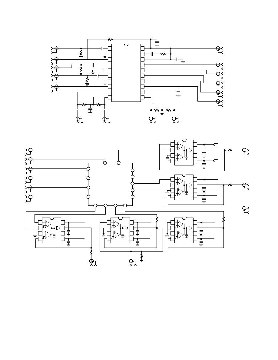
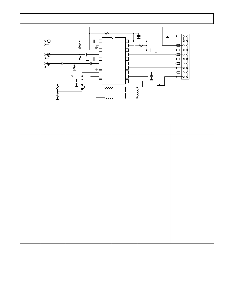
Figure 1. AD6459 Characterization Board
1
2
3
4
8
7
6
5
AD830
V
P
V
N
A=1
C7
0.1µF
V
N
R4
50
I
OUT
C6
0.1µF
V
P
C5
0.1µF
V
N
R3
50
I
OUT
C4
0.1µF
V
P
GAIN
1
2
3
4
8
7
6
5
AD830
V
P
V
N
A=1
FREF
VPOS
GREF
GREF
PRUP
LOIP
RFIP
MXOP
MXOM
IFIP
IFIN
IRXP
IRXN
QRXP
QRXN
GAIN
AD6459
CHARACTERIZATION
BOARD
PRUP
LOIP
RFIP
FREF
VPOS
C8
0.1µF
V
N
C9
0.1µF
V
P
1
2
3
4
8
7
6
5
AD830
V
P
V
N
A=1
R5
50
C10
0.1µF
V
N
C11
0.1µF
V
P
1
2
3
4
8
7
6
5
AD830
V
P
V
N
A=1
R6
50
IFIN
R1
50
C2
0.1µF
C3
0.1µF
1
2
3
4
8
7
6
5
AD830
V
P
V
N
A=1
V
N
V
P
MXOP
R2
50
Figure 2. Characterization Test Set
AD6459
5
REV. 0
RF FREQUENCY dB
20
6
50
450
100
SSB NF dB
150
200
250
300
350
400
18
14
12
10
8
16
R
IN
= 50
, IF = 13MHz
R
IN
= 50
, IF = 26MHz
R
IN
= 1k
, IF = 13MHz
R
IN
= 50
, F = 45MHz
R
IN
= 400
, IF = 13MHz
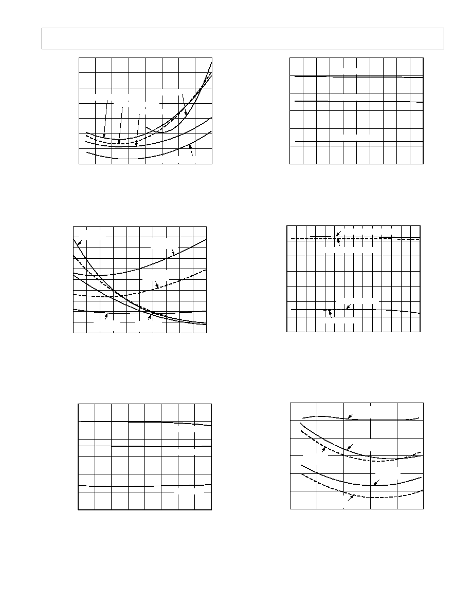
Figure 3. Mixer Noise Figure vs. RF Frequency
RF FREQUENCY MHz
RESISTANCE
2000
800
0
50
550
100
150
200
250
300
350
400
450
500
1800
1000
600
200
1400
1200
400
1600
R SHUNT
V
GAIN
= 2.2V
C SHUNT
V
GAIN
= 0.2V
C SHUNT
V
GAIN
= 1.0V
R SHUNT
V
GAIN
= 0.2V
C SHUNT
V
GAIN
= 2.2V
5.0
4.8
4.6
4.4
4.2
4.0
3.8
3.6
3.4
3.2
3.0
CAPACITANCE pF
Figure 4. Mixer Input Impedance vs. RF Frequency,
V
POS
= 2.7 V, T
A
= +25
°
C
RF FREQUENCY MHz
20
10
50
450
100
GAIN dB
150
200
250
300
350
400
15
10
5
0
5
V
GAIN
= 0.2V
V
GAIN
= 1.0V
V
GAIN
= 2.25V
Figure 5. Mixer Conversion Gain vs. RF Frequency,
T
A
= +25
°
C, V
POS
= 2.7 V, V
REF
= 1.2 V, F
IF
= 26 MHz
RF FREQUENCY MHz
20
10
6
38
10
GAIN dB
14
18
22
26
30
34
15
10
5
0
5
V
GAIN
= 0.2V
V
GAIN
= 1.0V
V
GAIN
= 2.25V
42
46
Figure 6. Mixer Conversion Gain vs. IF Frequency,
T
A
= +25
°
C, V
POS
= 2.7 V, V
REF
= 1.2 V, FRF = 250 MHz
TEMPERATURE
°
C
70
30
0
50
90
40
GAIN dB
20 10
0
10
20
30
40
50
60
70 80
60
50
20
10
40
30
AMP/DEMOD, V
POS
= 2.7V
AMP/DEMOD, V
POS
= 5.5V
MIXER, V
POS
= 2.7V
MIXER, V
POS
= 5.5V
Figure 7. Mixer Conversion Gain and IF Amplifier/
Demodulator Gain vs. Temperature, V
GAIN
= 0.2 V,
V
REF
= 1.2 V , F
IF
= 26 MHz, F
RF
= 250 MHz
GAIN VOLTAGE Volts
9
10
15
0
2.5
0.5
INPUT 1dB COMPRESSION POINT
REFERED TO 50
dBm
1
1.5
2
11
12
13
14
V
POS
= 5.5V
T
A
= +85
°
C
V
POS
= 5.5V
T
A
= +25
°
C
V
POS
= 2.7V
T
A
= +25
°
C
V
POS
= 2.7V
T
A
= 25
°
C
V
POS
= 5.5V
T
A
= 45
°
C
Figure 8. Mixer Input 1 dB Compression Point vs.
V
GAIN
, V
REF
= 1.2 V, F
RF
= 250 MHz, F
IF
= 26 MHz
AD6459
6
REV. 0
INTERMEDIATE FREQUENCY dB
70
0
5
45
10
15
20
25
30
35
40
60
40
30
20
10
50
V
GAIN
= 0.2V
V
GAIN
= 1.0V
V
GAIN
= 1.5V
V
GAIN
= 2.25V
IF AMP/DEMOD GAIN dB
Figure 9. IF Amplifier and Demodulator Gain vs.
Frequency, T
A
= +25
°
C, V
POS
= 2.7 V, V
REF
= 1.2 V
IF FREQUENCY MHz
12000
6000
0
0
100
10
RESISTANCE
20
30
40
50
60
70
80
90
10000
8000
4000
2000
R SHUNT, V
GAIN
= 2.2V
C SHUNT, VGAIN= 1.0V
R SHUNT, V
GAIN
= 1.0V
R SHUNT, V
GAINS
= 0.2V
C SHUNT, V
GAIN
= 2.2V
C SHUNT, V
GAIN
= 0.2V
3.5
3.0
2.5
2.0
1.5
1.0
0.5
CAPACITANCE pF
Figure 10. IF Amplifier Input Impedance vs.
Frequency, T
A
= +25
°
C, V
POS
= 2.7 V, V
REF
= 1.2 V
GAIN VOLTAGE Volts
INPUT 1dB COMPRESSION POINT
REFERED TO 50
dBm
5
10
55
0
2.5
0.5
1
1.5
2
25
40
45
50
15
20
35
30
Figure 11. IF Amplifier/Demodulator Input 1 dB
Compression Point vs. V
GAIN
, F
IF
= 19.5 MHz,
V
REF
= 1.2 V, T
A
= +25
°
C, V
POS
= 2.7 V
GAIN VOLTAGE Volts
1
0.8
0
0
2.5
0.5
1
1.5
2
0.2
0.6
0.8
1.0
0.6
0.4
0.4
0.2
MIXER
ERROR dB
IF AMP/DEMOD
Figure 12. AD6459 Gain Error vs. Gain Control
Voltage, Representative Part
FREF FREQUENCY MHz
QUADRATURE ERROR Degrees
3.0
0
5
45
10
15
20
25
30
35
40
2.5
2.0
1.5
1.0
0.5
Figure 13. Demodulator Quadrature Error vs.
F
REF
Frequency, T
A
= +25
°
C, V
POS
= 2.7 V
CARRIER FREQUENCY kHz
PHASE NOISE dBc
90
95
120
0.1
10k
1
10
100
1k
100
105
110
115
Figure 14. PLL Phase Noise vs. Frequency,
V
POS
= 3 V, C10 = 1 nF, F
REF
= 13 MHz
AD6459
7
REV. 0
PLL FREQUENCY MHz
FLTR PIN VOLTAGE
REFERENCED TO V
POS
Volts
0.1
1.5
5
55
10
15
20
25
30
35
40
45
50
0.3
0.5
0.7
0.9
1.1
1.3
Figure 15. PLL Loop Voltage at FLTR Pin (KVCO) vs.
Frequency
GAIN VOLTAGE Volts
10
INPUT 1dB COMPRESSION POINT
REFERED TO 50
dBm
20
80
0.5
2.5
1.0
1.5
2.0
40
50
60
70
30
Figure 16. System (Mixer + IF LC Filter +IF Amplifier +
Demodulator) 1 dB Compression Point vs. Gain,
T
A
= +25
°
C, V
POS
= 2.7 V, F
IF
= 13 MHz, V
REF
= 1.2 V
GAIN VOLTAGE Volts
10
20
0
0.5
2.5
1.0
1.5
2.0
40
50
60
70
30
INPUT IP3 REFERED TO 50
dBm
Figure 17. System (Mixer + IF LC Filter + I F Amplifier +
Demodulator) IP3 vs. Gain, T
A
= +25
°
C, V
POS
= 2.7 V,
IF = 13 MHz, V
REF
= 1.2 V
GAIN VOLTAGE Volts
SUPPLY CURRENT mA
18
16
4
0
2.5
0.5
1
1.5
2
12
10
8
6
14
V
POS
= 2.7V, T
A
= +85
°
C
V
POS
= 2.7V, T
A
= +25
°
C
V
POS
= 5.5V, T
A
= +85
°
C
V
POS
= 5.5V, T
A
= +25
°
C
V
POS
= 5.5V, T
A
= 40
°
C
Figure 18. Power Supply Current vs. Gain Control
Voltage, V
REF
= 1.2 V
AD6459
8
REV. 0
PRODUCT OVERVIEW
The AD6459 provides most of the active circuitry required to
realize a complete low power, single-conversion superhetero-
dyne receiver, or the latter part of a double-conversion receiver,
at input frequencies up to 500 MHz, with an IF from 5 MHz to
50 MHz. The internal I/Q demodulators, and their associated
phase-locked loop, support a wide variety of modulation modes,
including n-PSK, n-QAM and GMSK. A single positive supply
voltage of 3 V is required (2.7 V minimum, 5.5 V maximum) at
a typical supply current of 8 mA at midgain. In the following
discussion, V
POS
will be used to denote the power supply voltage,
which will be normally assumed to be 3 V.
Figure 20 shows the main sections of the AD6459. It consists of
a variable-gain UHF mixer and a linear two-stage IF strip,
which together provide a calibrated voltage-controlled gain range
of more than 76 dB, followed by dual quadrature demodulators.
These are driven by inphase and quadrature clocks that are
generated by a Phase-Locked Loop (PLL), which is locked to a
corrected external reference. A CMOS-compatible power-down
interface completes the AD6459.
Mixer
The UHF mixer is an improved Gilbert-cell design and can
operate from low frequencies (it is internally dc-coupled) up to
an RF input of 500 MHz. The dynamic range at the input of the
mixer is determined, at the upper end, by the maximum input
signal level of
±
90 mV (11 dBm in 50
between RFHI and
RFLO) up to which the mixer remains essentially linear, and at
the lower end, by the noise level. It is customary to define the
linearity of a mixer in terms of its 1 dB gain-compression point
and third-order intercept, which for the AD6459 are 11 dBm
and 0 dBm, respectively, in a 50
system.
The mixer's RF input port is differential; that is, pin RFLO is
functionally identical to RFHI, and these nodes are internally
biased. The RF port can be modeled as a parallel RC circuit as
shown in Figure 19.
RFHI
RFLO
C
SH
R
SH
Figure 19. Mixer Port Modeled as a Parallel RC Network
The local oscillator (LO) input is internally biased at V
P
0.8 V
and must be ac coupled. The LO interface includes a preampli-
fier that minimizes the drive requirements, thus simplifying the
oscillator design and reducing LO leakage from the RF port.
The LO requires a single-sided drive of
±
50 mV, or 16 dBm
in a 50
system. For operation above 300 MHz, noise figure
can be improved by increasing the LO level.
LC
BANDPASS
FILTER
PLL
VPS1
RFHI
AD6459
MXOP
MXOM
IFIP
IFIM
+
0
°
50
°
4.7k
4.7k
4.7k
4.7k
GAIN TO
COMPENSATION
AGC VOLTAGE
BIAS
CIRCUIT
VPS2
PRUP
RFLO
LOIP
IRXP
IRXN
FREF
FLTR
QRXP
QRXN
GAIN
GREF
19
20
13
14
15
16
17
18
6
7
8
1
2
3
4
5
COM1
COM2
9
10
11
12
Figure 20. Functional Block Diagram
AD6459
9
REV. 0
The output of the mixer is differential. The nominal conversion
gain is specified for operation into a 19.5 MHz LC IF bandpass
filter as shown in Figure 21 and Table I.
The conversion gain is measured between the mixer input and
the input of this filter and varies between 5 dB and +15 dB.
MXOP
MXOM
C2
L1
C1
C1
IFIP
IFIM
Figure 21. Suggested IF Filter Inserted Between the
Mixer's Output Port and the Amplifier's Input Port
Table I. Filter Component Values for Selected Frequencies
Frequency
C1
L1
C2
13 MHz
27 pF
0.82
µ
H
180 pF
19.5 MHz
27 pF
0.56
µ
H
110 pF
26 MHz
22 pF
0.39
µ
H
82 pF
40 MHz
22 pF
0.12
µ
H
100 pF
The maximum permissible signal level between MXOP and
MXOM is determined by the maximum gain control voltage.
The mixer output port, having pull-up resistors of 250
to
V
POS
, is shown in Figure 22.
MXOP
MXOM
250
250
V
POS
Figure 22. Mixer Output Port
IF Amplifier
Most of the gain in the AD6459 is provided by the IF amplifier
strip, which comprises two stages. Both are fully differential and
each has a gain span of 26 dB for the AGC voltage range of 0.2
V to 2.25 V. Thus, in conjunction with the variable gain of the
mixer, the total gain span is 76 dB. The overall IF gain varies
from 13 dB to 45 dB for the nominal AGC voltage of 0.2 V to
2.25 V. Maximum gain is at V
GAIN
= 0.2 V.
The IF input is differential, at IFIP and IFIM. Figure 23 shows
a simplified schematic of the IF interface modeled as parallel
RC network.
The IF's small-signal bandwidth is approximately 50 MHz from
IFIP and IFIM through the demodulator.
IFHI
IFLO
C
SH
R
SH
Figure 23. IF Amplifier Port Modeled as a Parallel RC
Network
Gain Scaling
The AD6459's overall gain, expressed in decibels, is linear with
respect to the AGC voltage V
GAIN
at pin GAIN. The gain of all
sections is maximum when V
GAIN
is 0.2 V and falls off as the
bias is increased to V
GAIN
= 2.25 V. The gain is independent
of the power supply voltage. The gain of all stages changes
simultaneously. The AD6459's gain scaling is also tempera-
ture compensated.
Note that GAIN pin of the AD6459 is an input driven by an
external low impedance voltage source, normally a DAC, under
the control of the radio's digital processor.
The gain-control scaling is directly proportional to the reference
voltage applied to the pin GREF and is independent of the
power supply voltage. When this input is set to the nominal
value of 1.2 V, the scale is nominally 27 mV/dB (37 dB/V).
Under these conditions, 76 dB of gain range (mixer plus IF)
corresponds to a control voltage of 0.2 V
V
GAIN
2.25 V.
The final centering of this 2.05 V range depends on the inser-
tion losses of the IF filters used.
Pin GREF can be tied to an external voltage reference (V
REF
)
provided, for example, by an AD1580 (1.21 V) voltage reference.
When using the Analog Devices AD7013 (IS54, TETRA, and
satellite receiver applications) and AD7015 or AD6421 (GSM,
DCS1800, PCS1900) baseband converters, the external refer-
ence may also be provided by the reference output of the
baseband converters. The interface between the AD6459 and
the AD6421 baseband converter is shown in Figure 24. The
AD7015 baseband converter provides a V
R
of 1.23 V. An auxil-
iary DAC in the AD7015 can be used to generate the AGC
voltage. Since it uses the same reference voltage, the numerical
input to this DAC provides an accurate RSSI value in digital
form, no longer requiring the reference voltage to have high
absolute accuracy.
AD6459
IRXP
IRXN
QRXP
QRXP
GREF
GAIN
FREF
AD6421
100pF
100pF
100pF
100pF
0.1µF
160
1nF
VCTCXO
IRXP
IRXP
IRXP
IRXN
BREFOUT
BREFCAP
AGC DAC
AFC DAC
Figure 24. Interfacing the AD6459 to the AD6421
Baseband Converter
AD6459
10
REV. 0
I/Q Demodulators
Both demodulators (I and Q) receive their inputs internally
from the IF amplifiers. Each demodulator comprises a full-wave
synchronous detector followed by an 8 MHz, two-pole low-pass
filter, producing differential outputs at pins IRXP and IRXN,
and QRXP and QRXN. Using the I and Q demodulators for
IFs above 50 MHz is precluded by the 5 MHz to 50 MHz range
of the PLL used in the demodulator section.
The I and Q outputs are differential and can swing up to
2.2 V p-p at the low supply voltage of 2.7 V. They are nominally
centered at 1.5 V, independent of power supply. They can
therefore directly drive the RX ADCs in the AD7015 baseband
converter, which require an amplitude of 1.23 V to fully load
them when driven by a differential signal. The conversion gain
of the I and Q demodulators is 17 dB.
For IFs of less than 8 MHz, the on-chip low-pass filters (8 MHz
cutoff) do not adequately attenuate the IF or feedthrough
products; thus, the maximum input voltage must be limited to
allow sufficient headroom at the I and Q outputs for not only
the desired baseband signal but also the unattenuated higher-
order demodulation products. These products can be removed
by an external low-pass filter. A simple 1-pole RC filter with its
corner above the modulation bandwidth is sufficient to attenu-
ate undesired outputs. The design of the RC filter is eased by
the 4.7 k
resistor integrated at each I and Q output pin.
Phase-Locked Loop
The demodulators are driven by quadrature signals that are
provided by a variable-frequency quadrature oscillator (VFQO),
phase-locked to a reference signal applied to pin FREF. When
this signal is at the IF, inphase and quadrature baseband
outputs are generated at the I output (IRXP and IRXN) and Q
output (QRXP and QRXN), respectively. The quadrature
accuracy of this VFQO is typically within
±
1.5
°
at 19.5 MHz. A
simplified diagram of the FREF input is shown in Figure 25.
FREF
20k
5k
50µA PTAT
V
POS
5k
Figure 25. Simplified Schematic of the FREF interface
The VFQO operates from 5 MHz to 50 MHz and is controlled
by the voltage between VPOS and FLTR. In normal operation a
series RC network, forming the PLL loop filter, is connected
from FLTR to V
POS
. The use of an integral sample-hold system
ensures that the frequency-control voltage on pin FLTR remains
held during power-down, so reacquisition of the carrier occurs
in less than 80
µ
s.
In practice, the probability of a phase mismatch at power-up is
high, so the worst case linear settling period to full lock needs to
be considered in making filter choices. This is typically < 80
µ
s for
a quadrature phase error of
±
3
°
at an IF of 19.5 MHz. Note that
the VFQO always provides quadrature between its own I and Q
outputs, but the phasing between it and the reference carrier
will swing around the final value during the PLL's settling time.
Bias System
The AD6459 operates from a single supply (V
POS
) usually 3 V,
at a typical supply current of 8 mA at midgain and T
A
= +25
°
C,
corresponding to a power consumption of 24 mW. Any voltage
from 2.7 V to 5.5 V may be used.
The bias system includes a fast-acting active high CMOS-
compatible power-up switch, allowing the part to idle at 2
µ
A
when disabled. Biasing is generally proportional-to-absolute-
temperature (PTAT) to ensure stable gain with temperature.
Other special biasing techniques are used to ensure very
accurate gain, stable over the full temperature range.
USING THE AD6459
In this section, we will focus on a few areas of special impor-
tance and include a few general application tips. As with any
wideband high gain component, great care is needed in PC
board layout. The location of the particular grounding points
must be considered with due regard to the possibility of
unwanted signal coupling.
The high sensitivity of the AD6459 leads to the possibility that
unwanted local EM signals may have an effect on the perfor-
mance. During system development, carefully-shielded test
assemblies should be used. The best solution is to use a fully
enclosed box enclosing all components with the minimum
number of needed signal connectors (RF, LO, I and Q outputs)
in miniature coax form.
Gain Distribution
As with all receivers, the most critical decisions in effectively
using the AD6459 relate to the partitioning of gain between the
various subsections (Mixer, IF Amplifier/Demodulator) and the
placement of filters to achieve the highest overall signal-to-noise
ratio and lowest intermodulation distortion.
Figure 26 shows an example of the main RF/IF signal path at
maximum and minimum signal levels.
SIGNAL LEVEL
IN dBm
10
20
30
40
50
60
70
80
90
100
MIXER
CONVERSION
GAIN
3dB
FILTER GAIN
IF
GAIN
DEMOD.
CONV.
GAIN
I
Q
CONSTANT
BASEBAND
OUTPUT
35mV
36dBm
16dBm
19dBm
76dBm
79dBm
19dBm
22dBm
79dBm
82dBm
15dBm
19dBm
95dBm
99dBm
IF INPUT
250 MHz
Figure 26. Signal Levels and Gain, Showing 76 dB Typical
and 80 dB Maximum Range in an Example Application
AD6459
11
REV. 0
14
13
12
11
17
16
15
20
19
18
10
9
8
1
2
3
4
7
6
5
AD6459
FREF
IRXP
VPS2
FLTR
VPS1
COM1
PRUP
LOIP
QRXN
QRXP
IRXN
RFLO
RFHI
COM2
GREF
MXOP
MXOM
IFIP
IFIM
GAIN
R1
20k
VPOS
C1
0.1µF
C10 1nF
R8 1k
C11
0.1µF
C9
10nF
FREF
R9
50
R2
50
LOIP
RFHI
GREF
R3
50
C12
1nF
C4 1nF
C7
1nF
VPOS
IRXP
QRXN
QRXP
IRXN
GAIN
C2
1nF
C3
SHORT
C5
0.1µF
JUMPER
VPOS
R6
24.9k
R7
16.9k
L3
SHORT
C16
22pF
C15
110pF
L2
0.56µH
PRUP
GND
GREF
L4
SHORT
C17
22pF
Figure 27. Evaluation Board as Received with 19.5 MHz Filter
Table II. AD6459 Evaluation Board Input and Output Connection
Reference
Connector
Approximate
Designation
Type
Description
Coupling
Signal Level
Comments
RFHI
SMA
RF Input
AC
11 dBm max
Input Is Terminated
in 50
LOIP
SMA
LO Input
AC
500 mV p-p max
Input Is Terminated
in 50
FREF
SMA
Demodulator Reference
AC
100 mV p-p min
Input Is Terminated
Input
in 50
MXOP
SMA
Mixer Output
NA
NA
Not Connected
for Unbalanced Output
Use XFMR
IFIP
SMA
IF Input
NA
NA
Not Connected
for Unbalanced Output
Use XFMR
J1
Jumper
On-Board GREF Bias
DC
0.4 V
POS
Two Resistors Divider
GREF
J2-1
External Reference Input
DC
1.2 V dc
Gain Scaling Reference
from External ADC
GAIN
J2-2
Gain Bias Input
DC
0.2 V to 2.4 V dc
Maw Gain at 0.2 V
QRXN
J2-3
Q-Negative Output
DC2 MHz
NA
Z Series = 4.7 k
QRXP
J2-4
Q-Positive Output
DC2 MHz
NA
Z Series = 4.7 k
IRXN
J2-5
I-Negative Output
DC-2 MHz
NA
Z Series = 4.7 k
IRXP
J2-6
I-Positive Output
DC-2 MHz
NA
Z Series = 4.7 k
VPOS
J2-7
Power Supply
DC
2.7 V to 5.5 V
Supply Voltage
Positive Input
PRUP
J2-8
Power Up
DC-2 MHz
CMOS
If Left Unconnected,
Board Is Active
GND
J2-J9
Ground
DC
0 V
NA
GND
J2-10
Ground
DC
0 V
NA
AD6459
12
REV. 0
C22041210/96
PRINTED IN U.S.A.
AD6459 EVALUATION BOARD
The AD6459 evaluation board (Figure 27) consists of a
AD6459, ground plane, I/O connectors, and a 19.5 MHz band
pass filter. The RF, LO and FREF ports are terminated in 50
to provide a broadband match or external signal generators.
The board provides SMA connectors for the RF, LO, demodu-
lator reference, mixer output and IF input signals. The MXOP
and IFIP connectors are left unconnected and are provided as a
testing convenience. Footprints for broadband matching trans-
formers and matching components are also provided to aid in
stage breakout testing.
The remaining low frequency signals, including the I and Q
interface, bias and power connections are made via a dual row
pin header that acts as an Interface Connector located along the
edges of the board. An on-board gain-reference 1.2 V biasing
option is provided via a single jumper, J1. The evaluation board
will not function without this jumper unless an external bias
GREF is provided from an external reference that is normally
provided by the associated ADC.
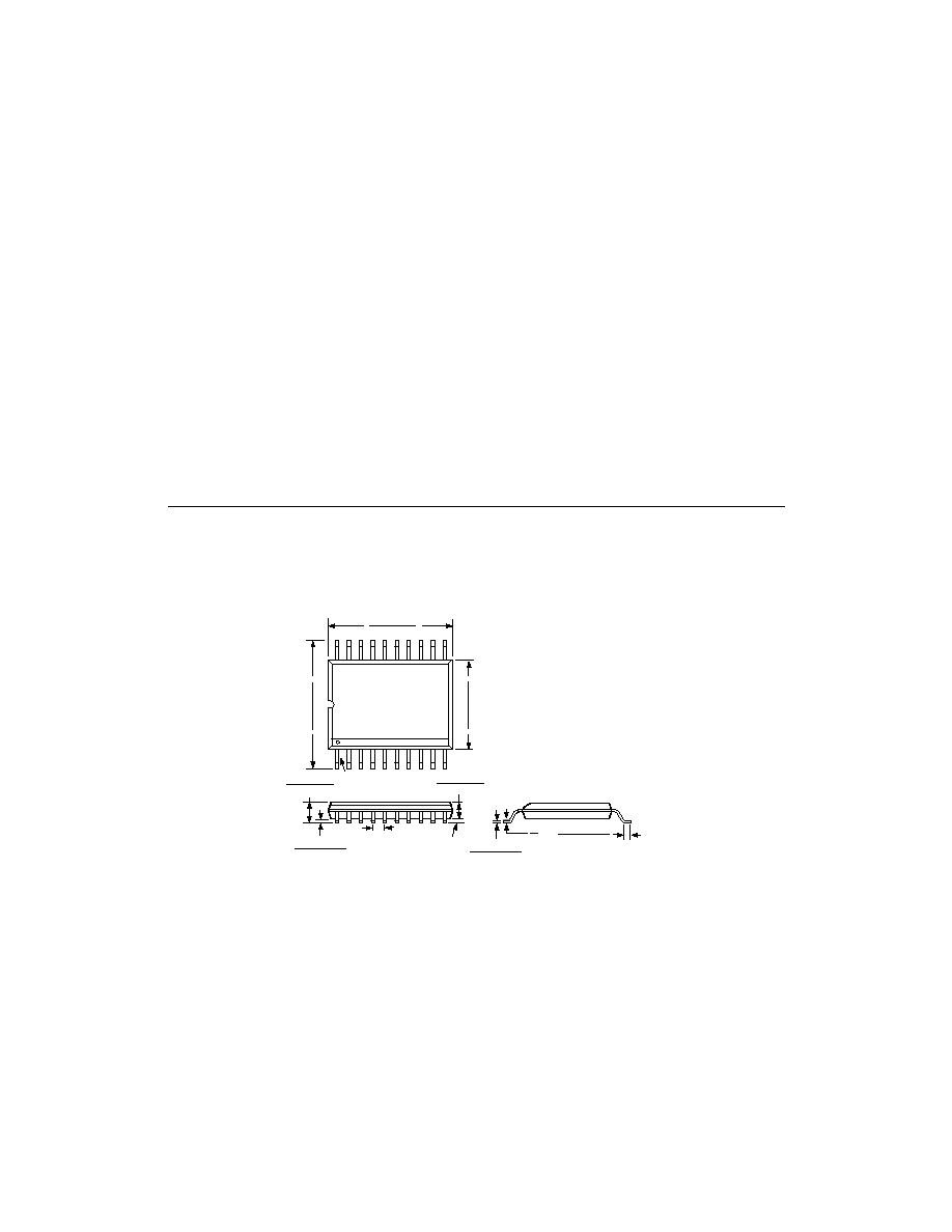
OUTLINE DIMENSIONS
Dimensions shown in inches and (mm).
20
11
10
1
0.295 (7.50)
0.271 (6.90)
0.311 (7.9)
0.301 (7.64)
0.212 (5.38)
0.205 (5.21)
PIN 1
SEATING
PLANE
0.008 (0.203)
0.002 (0.050)
0.07 (1.78)
0.066 (1.67)
0.0256
(0.65)
BSC
0.078 (1.98)
0.068 (1.73)
0.009 (0.229)
0.005 (0.127)
0.037 (0.94)
0.022 (0.559)
8
°
0
°
Full Path Configuration
As received, the board is configured for full-path evaluation
from RFHI to the I and Q outputs. The one-pole LC resonant
circuit provided represents a simple, yet balanced, IF bandpass
filtering approach. The filter supplied is centered at 19.5 MHz,
a common GSM intermediate frequency. Table I highlights the
filter component values for other IF frequencies. RFHI and
RFLO are true differential inputs, however for testing conve-
nience, the RFLO terminal of the AD6459 is ac referenced to
ground on the evaluation board. The GAIN bias input, which is
bypassed with a 10 nF capacitor, is brought out to the interface
connector. The PRUP input is provided with a 20 k
pull up
resistor to V
POS
that activates the board.
The four differential I and Q outputs are brought out uncondi-
tioned, directly to the interface connector. A high impedance,
high bandwidth FET-type probe should be used when measur-
ing the I and Q ports. Excessive capacitive or resistive loading of
these ports will severely limit the video bandwidth and signal
swing. The demodulator PLL filter installed on the evaluation
board (R8, C10) can accommodate the full VFQO lock range
specified.