 | ÐлекÑÑоннÑй компоненÑ: AD6472 | СкаÑаÑÑ:  PDF PDF  ZIP ZIP |
Äîêóìåíòàöèÿ è îïèñàíèÿ www.docs.chipfind.ru
REV. 0
Information furnished by Analog Devices is believed to be accurate and
reliable. However, no responsibility is assumed by Analog Devices for its
use, nor for any infringements of patents or other rights of third parties
which may result from its use. No license is granted by implication or
otherwise under any patent or patent rights of Analog Devices.
a
AD6472
One Technology Way, P.O. Box 9106, Norwood, MA 02062-9106, U.S.A.
Tel: 781/329-4700
World Wide Web Site: http://www.analog.com
Fax: 781/326-8703
© Analog Devices, Inc., 1998
2 Pair/1 Pair ETSI Compatible
HDSL Analog Front End
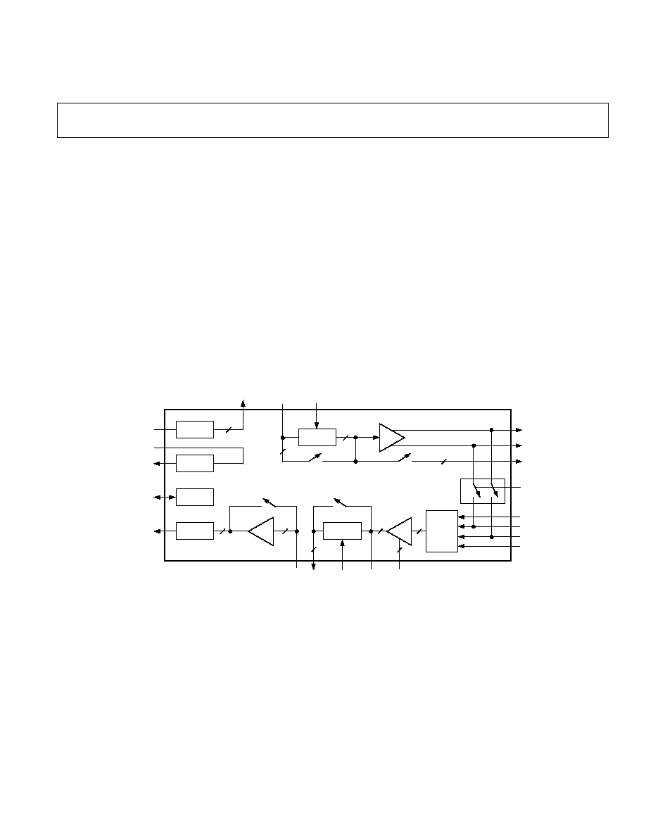
FUNCTIONAL BLOCK DIAGRAM
CONTROL
LOGIC
12-BIT
DAC
2
7-BIT
DAC
12-BIT
ADC
2
BUFFER
2
ANALOG
FILTER
2
PGA
2
HYBRID
CIRCUIT
2
ANALOG
FILTER
2
DRIVER
2
2
TX_GAIN
TO
VCXO
T
X
R
X
3
AD6472
FEATURES
Integrated Front End for Single Pair or Two Pair HDSL
Systems
Meets ETSI Specifications
Supports 1168 Kbps and 2.32 Mbps
Transmit and Receive Signal Path Functions
Receive Hybrid Amplifier, PGA and ADC
Transmit DAC, Filter and Differential Outputs
Programmable Filters
Control and Ancillary Functions
Timing Recovery DAC
Normal Loopback and Low Power Modes
Simple Interface-to-Digital Transceivers
Single 5 V Power Supply
Power Consumption: 320 mW--(Excluding Driver)
Package: 80-Lead MQFP
Operating Temperature: 40 C to +85 C
GENERAL DESCRIPTION
The AD6472 is a single chip analog front end for two pair or
single pair HDSL applications that use 1168 Kbps or 2.32 Mbps
data rates.
The AD6472 integrates all the transmit and receive functional
blocks together with the timing recovery DAC.
The digital interface is designed to support industry standard
digital transceivers.
While providing the full analog front end for ETSI standards
(two pair or single pair HDSL applications) the AD6472 sup-
ports other applications because the architecture allows for
bypassing the functional blocks.
The normal, low power, and loopback modes and the digital
interface combine to make the AD6472 simple to integrate into
systems.

2
REV. 0
AD6472SPECIFICATIONS
(T
A
= T
MIN
to T
MAX
unless otherwise noted)
P
arameter
Min
Typ
Max
Units
Condition
TRANSMIT CHANNEL
SNR
68
71
dB
The complete transmit path spectrum and pulse
THD
66
71
dB
shape comply with ETSI requirements.
TRANSMIT DAC
The transmit DAC maximum update rate is half
Clock Frequency
18.688
MHz
the maximum output data rate, i.e., 1168 kHz.
Resolution
12
Bits
The maximum transmit clock is 16
×
1168 =
Update Rate
1168
kHz
18.688 MHz.
Output Voltage
2
V p-p Diff
TRANSMIT FILTER
Corner Frequency (3 dB)
1
320
kHz
MODE_SEL1 = 0
535
kHz
MODE_SEL1 = 1
Accuracy
±
5
±
10
%
Gain
9.53
dB
3.53
dB
LINE DRIVER
VCM
2.5
V
Transformer Turns Ratio = 1:2.3 at 50 kHz
Output Power
13.5
dBm
When Loaded by ETSI (RTR/TM3036)
Output Voltage
6
V p-p Diff
HDSL Test Loops
TRANSMIT VOLTAGE LEVEL
6
V p-p Diff
TX_GAIN = 0
3
V p-p Diff
TX_GAIN = 1
RECEIVE CHANNEL
SNR
68
71
dB
THD
66
71
dB
HYBRID INTERFACE
V
CM
= 2.5 V. See Figure 3
Input Voltage Range
5
V p-p Diff
Input Impedance
10
k
PROGRAMMABLE GAIN AMPLIFIER
Condition 6 dB to +9 dB
Overall Gain Accuracy
±
1
dB
Gain Step
3
dB
Gain Step Accuracy
±
0.25
dB
RECEIVE FILTER
Corner Frequency (3 dB)
1
320
kHz
MODE_SEL1 = 0
640
kHz
MODE_SEL1 = 1
Accuracy
±
5
±
10
%
TIMING RECOVERY DAC
Resolution
7
Bits
Guaranteed Monotonic
Output Low
0.5
V
Output High
4.5
V
DIGITAL INTERFACE
5 V Supply, V
MIN
to V
MAX
Input Logic High, V
IH
3.3
V
Input Logic L
OW
, V
IL
0.8
V
Output Logic High, V
OH
V
DD
0.3
V
Output Logic Low, V
OL
0.4
V
3.3 V Supply, V
MIN
to V
MAX
Input Logic High, V
IH
2.0
V
Input Logic Low, V
IL
0.2
V
Output Logic High, V
OH
V
DD
0.3
V
POWER SUPPLY VOLTAGE
V
MIN
to V
MAX
4.75
5
5.25
V
5 V Supply
3.15
3.3
3.45
V
3.3 V Supply
POWER SUPPLY CURRENT
V
MIN
to V
MAX
, T
MIN
to T
MAX
Normal Mode, Excl. Driver
65
mA
5 V Supply, MODE_SEL1 = 0
OVRSAMP Mode
73
mA
5 V Supply, MODE_SEL1 = 1, MODE_SEL0 = 1
Line Driver
50
mA
With 50
Differential Load
Low Power Mode
17
mA
OPERATING TEMPERATURE RANGE
40
+85
°
C
T
MIN
to T
MAX
NOTES
1
The ADC clock period t(1
÷
f) is used for the dynamic tuning of the Tx and Rx filters.
Specifications subject to change without notice.
AD6472
3
REV. 0
ORDERING GUIDE
Temperature
Package
Package
Model
Range
Description
Option
AD6472BS
40
°
C to +85
°
C
80-Lead Plastic Quad Flatpack
S-80A
ABSOLUTE MAXIMUM RATINGS
*
Supply Voltage . . . . . . . . . . . . . . . . . . . . . . . . 0.3 V to +6.0 V
Input Voltage . . . . . . . . . . . . . . . . . . . . 0.5 V to V
DD
+ 0.5 V
Output Voltage Swing . . . . . . . . . . . . . 0.5 V to V
DD
+ 0.5 V
Operating Temperature Range (Ambient) . . . 40
°
C to +85
°
C
Storage Temperature Range . . . . . . . . . . . . 65
°
C to +150
°
C
Lead Temperature (5 sec) MQFP . . . . . . . . . . . . . . . . +280
°
C
*Stresses above those listed in this section may cause permanent damage to the
device. This is a stress rating only, functional operation of the device at these or
any other conditions above those in the operation section of this specification is
not implied. Exposure to absolute maximum rating conditions for extended
periods may affect device reliability.
Thermal Characteristics
80-Lead Plastic Quad Flatpack Package . . . . . . .
JA
= 45
°
C/W
CAUTION
ESD (electrostatic discharge) sensitive device. Electrostatic charges as high as 4000 V readily
accumulate on the human body and test equipment and can discharge without detection.
Although the AD6472 features proprietary ESD protection circuitry, permanent damage may
occur on devices subjected to high energy electrostatic discharges. Therefore, proper ESD
precautions are recommended to avoid performance degradation or loss of functionality.
WARNING!
ESD SENSITIVE DEVICE
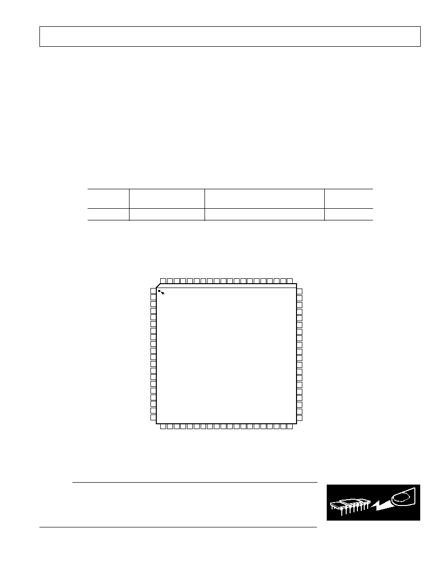
PIN CONFIGURATION
80 79 78 77 76
71 70 69 68 67 66 65
75 74 73 72
64 63 62 61
1
2
3
4
5
6
7
8
9
10
11
13
14
15
16
12
17
18
20
19
60
59
58
57
56
55
54
53
52
51
50
49
48
47
46
45
44
43
42
41
21 22 23 24 25 26 27 28 29 30 31 32 33 34 35 36 37 38 39 40
PIN 1
IDENTIFIER
TOP VIEW
(Not to Scale)
RXCLK
RX11
RX10
RX9
RX8
RX7
RX6
+3V_DVDD
DGND
RX5
RX4
RX3
RX2
RX1
RX0
SCLK
+5V_DVDD
DGND
MODE_SEL0
MODE_SEL1
AA_FLTR_BP
PWRDN
NC
TX_GAIN_SEL
TX_DRVR_BP
ADC_BUF_BP
TX_LPF_BP
TSTGND
LOOPBACK
DGND
+3V_DVDD
TX_DATA
NC
+5V_DVDD
DGND
AVDD
AGND
CM_LVL
VREF
CAP_BOT
CAP_TOP
REF_COM
ADC_INA
ADC_INB
AA_FLTR_OUTA
AA_FLTR_OUTB
PGA_GC0
PGA_GC1
NC
IOUT_SET
NC
CAP_B
CAP_C
TX_IOUT_A
TX_IOUT_B
AGND
AVDD
TX_LPF_IN_B
TX_LPF_OUT_B
TX_LPF_OUT_A
AVDD
DRVR_OUT_B
DRVR_OUT_A
TX_LPF_IN_A
AD6472
S-80A
SFRAME
SDATA
TR_DAC_OUT
+3V_DVDD
PGA_GC2
AVDD
AGND
HYB_IN1_A
AGND
HYB_IN2_B
HYB_IN2_A
HYB_IN1_B
TX_SYNC
TX_CLK
+5V_DVDD
DGND
NC = NO CONNECT

AD6472
4
REV. 0
Pin
Mnemonic
Description
1
+5 V_DVDD
+5 V Digital Supply.
2
DGND
Digital Ground.
3
MODE_SEL0
Bit Rate--Filter Corner Select.
4
MODE_SEL1
Bit Rate--Filter Corner Select.
5
AA_FLTR_BP
Antialiasing Filter Bypass.
6
PWRDN
Power-Down Active Low.
7
NC
No Connect.
8
TX_GAIN_SEL
Transmit Attenuation (6 dB) Select.
9
TX_DRVR_BP
Transmit Driver Bypass.
10
ADC_BUF_BP
ADC Buffer Bypass.
11
TX_LPF_BP
Transmit Filter Bypass.
12
TSTGND
Factory test pin. Connect to DGND.
13
LOOPBACK
Loopback Select.
14
DGND
Digital Ground.
15
+3 V_DVDD
+3.3 V Digital Supply.
16
TX_DATA
Transmit Data Input.
17
TX_SYNC
Transmit Data Frame Sync Input.
18
TX_CLK
Transmit Clock Input.
19
+5 V_DVDD
+5 V Digital Supply.
20
DGND
Digital Ground.
21
NC
No Connect.
22
IOUT_SET
DAC Output Current Full Scale
(With Resistor to Ground).
23
NC
No Connect.
24
CAP_B
Decoupling Pin for Internal Node.
25
CAP_C
Decoupling Pin for Internal Node.
26
TX_IOUT_A
TXDAC Complementary Current
Output.
27
TX_IOUT_B
TXDAC Complementary Current
Output.
28
AGND
Analog Ground.
29
AVDD
+5 V Analog Supply.
30
TX_LPF_IN_B
Differential Input to LPF.
31
TX_LPF_IN_A
Differential Input to LPF.
32
TX_LPF_OUT_B
Differential Output from Transmit
(If Driver Bypassed).
33
TX_LPF_OUT_A Differential Output from Transmit
(If Driver Bypassed).
34
AVDD
+5 V Analog Supply.
35
DRVR_OUT_B
Differential Driver Output.
36
DRVR_OUT_A
Differential Driver Output.
37
AGND
Analog Ground.
38
HYB_IN2_B
Hybrid Noninverting Input.
39
HYB_IN2_A
Hybrid Noninverting Input.
40
HYB_IN1_B
Hybrid Inverting Input.
PIN CONFIGURATIONS
Pin
Mnemonic
Description
41
HYB_IN1_A
Hybrid Inverting Input.
42
AGND
Analog Ground.
43
AVDD
+5 V Analog Supply.
44
PGA_GC2
PGA Gain Select Bits.
45
PGA_GC1
PGA Gain Select Bits.
46
PGA_GC0
PGA Gain Select Bits.
47
AA_FLTR_OUTB Differential Output of the
Antialiasing Filter.
48
AA_FLTR_OUTA Differential Output of the
Antialiasing Filter.
49
ADC_INB
Differential Input to the ADC.
50
ADC_INA
Differential Input to the ADC.
51
REF_COM
Reference Common.
52
CAP_TOP
Decoupling Pin for ADC Reference.
53
CAP_BOT
Decoupling Pin for ADC Reference.
54
VREF
External Voltage Reference.
55
CM_LVL
Common-Mode Level.
(1/2 Supply Voltage, Nominally.)
56
AGND
Analog Ground.
57
AVDD
+5 V Analog Supply.
58
DGND
Digital Ground.
59
+5 V_ DVDD
+5 V Digital Supply.
60
NC
No Connect.
61
+3 V_ DVDD
+3 V Digital Supply.
62
TR_DAC_OUT
Timing Recovery DAC Output
Voltage.
63
SDATA
Serial Data Input to Timing Recov-
ery DAC.
64
SFRAME
Frame Sync for Timing Recovery.
65
SCLK
Clock for Timing Recovery DAC.
Serial Data.
66
RX0
Digital Output Data.
67
RX1
Digital Output Data.
68
RX2
Digital Output Data.
69
RX3
Digital Output Data.
70
RX4
Digital Output Data.
71
RX5
Digital Output Data.
72
DGND
Digital Ground.
73
+3 V_DVDD
+3 V Digital Supply.
74
RX6
Digital Output Data.
75
RX7
Digital Output Data.
76
RX8
Digital Output Data.
77
RX9
Digital Output Data.
78
RX10
Digital Output Data.
79
RX11
Digital Output Data.
80
RXCLK
Clock Input for ADC Data.
AD6472
5
REV. 0
Circuit Description
The AD6472 is an HDSL analog front end for either 2-pair or
single pair applications.
Transmit Channel
The AD6472 receives, from a DSP transceiver core, a serial 2s
complement data stream. The data are 16-bit words and the
MSB is received first.
The 12-bit DAC converts the digital data to an analog signal.
Although HDSL uses four level 2B1Q modulation, the 12-bit
DAC is necessary because of the linearity requirements of the
echo canceling circuit.
The active filters have dynamic tuning and selectable filter
corners that meet transmit mask requirements for both two-pair
and single pair applications. A 6 dB attenuation option is in-
cluded as part of the filter to increase the driver output dynamic
range. Bypassing the active filter means giving up the 6 dB
option, and reduces the maximum TX output voltage to
2 V p-p diff.
The filtered transmit signal is then processed by the driver
amplifier. The DAC output controls the driver output level.
The designer can choose to bypass the driver amplifier; in this
case the driver amplifier will be powered down, and the TX
output will be at the TX_LPF_OUT pins.
The AD6472 meets the requirements of the ETSI masks (both
frequency and time domains for pulse shape). This includes the
worst case in RTR/TM 3036.
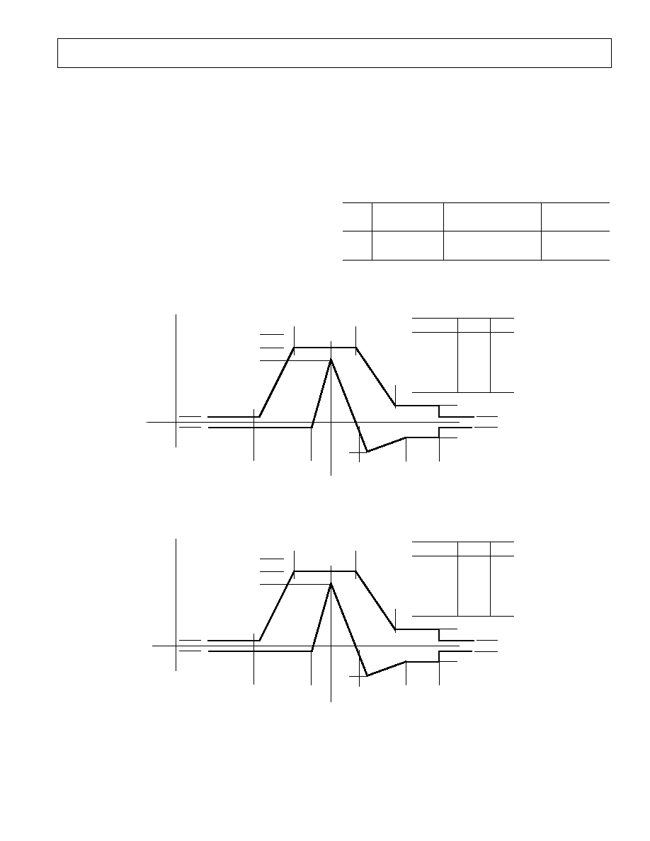
Table I. Transmit Spectra
Rate
Nyquist Frequency
Time Interval
Kbps
Application
kHz
T ( s)
1168
2-Pair E1
292
1710
2320
Single Pair E1
580
862
B
C
D
0.4T
0.4T
A
F
1.2T
0.6T
0.5T
14T
50T
H
E
F
A
G
1.25T
PARAMETER
VALUE
%
A
B
C
D
E
F
G
H
0.0264
2.8248
2.64
2.4552
0.0792
0.0264
0.4224
0.1320
1
107
100
93
3
1
16
5
0
Figure 1. 2-pair Transmit Pulse Shape Mask Normalized
B
C
D
0.4T
0.4T
A
F
1.2T
0.6T
0.5T
14T
50T
H
E
F
A
G
1.25T
PARAMETER
VALUE
%
A
B
C
D
E
F
G
H
0.0250
2.6750
2.500
2.3250
0.104
0.0250
0.5000
1.250
1
107
100
93
4
1
20
5
0
Figure 2. Single Pair Transmit Pulse Shape Mask Normalized
AD6472
6
REV. 0
Table III.
Receive Channel
Filter Control Bit
Receive Clock
3 dB Frequency
MODE_SEL1
MODE_SEL0
Frequency (kHz)
(kHz)
0
0
1168/2
Rx = 320/Tx = 320
0
1
Reserved
Reserved
1
0
1160
Rx = 640/Tx = 535
1
1
1160
×
2
Rx = 640/Tx = 535
Table IV. Configuration Control
Pin
Mnemonic
Logic 0 = Function
Logic 1 = Function
5
AA_FLTR_BP
Receive Filter in Circuit
Receive Filter Bypassed
6
PWRDN
Low Power Selected
Normal Operating Mode
7
ADC_BUF_BP
ADC Buffer in Circuit
ADC Buffer Bypassed
8
TX_GAIN_SEL
0 dB Attenuation
6 dB Attenuation
9
TX_DRVR_BP
Line Driver in Circuit
Line Driver Bypassed
11
TX_LPF_BP
Transmit Filter in Circuit
Transmit Circuit Bypassed
13
LOOPBACK
Normal Operation
Analog Loopback Selected
Receive Channel
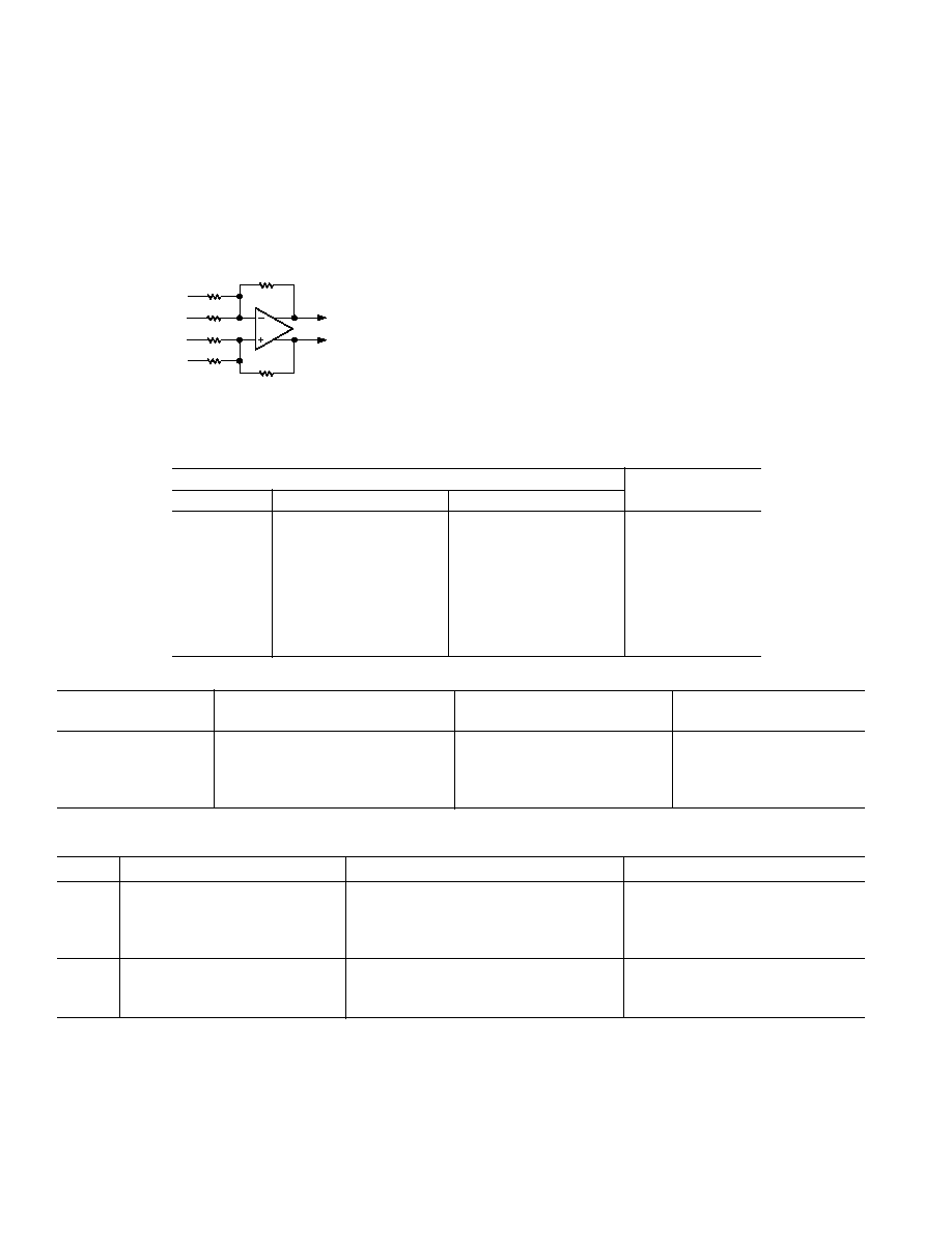
Hybrid Amplifier
The hybrid amplifier performs balanced to unbalanced
conversion.
Programmable Gain Amplifier (PGA)
The PGA can be programmed to amplify the receive signal
from between 6 dB and 9 dB. Refer to Table II for PGA gain
control information.
10k
10k
10k
10k
10k
10k
TO PGA
HYB_IN1_A
HYB_IN1_B
HYB_IN2_A
HYB_IN2_B
Figure 3.
Transmit and Receive Filters
Refer to Table III for transmit and receive channels filter
control information. The receive channel filters meet ETSI
requirements.
Analog-to-Digital Converter (ADC)
The receive channel ADC has a pipeline architecture with 12-
bit resolution. The ADC can be clocked at 2320 kHz, maxi-
mum. Output data is provided in 2s complement form.
Timing Recovery D/A
The AD6472 has an integrated D/A converter to control an
external VCXO used for timing recovery. The D/A is 7 bits and
monotonic. The D/A accepts 7 bits inverted format input data
serially with the MSB first.
Configuration Control
Table IV presents control information that you use to configure
the AD6472.
Table II.
Gain Control Bit
Binary Count
PGA_GC2
PGA_GC1
PGA_GC0
GAIN (dB)
0
0
0
6
0
0
1
3
0
1
0
0
0
1
1
3
1
0
0
6
1
0
1
9
1
1
0
9
1
1
1
9
AD6472
7
REV. 0
Table VI. 40% to 60% Duty Cycle RXCLK Clock
when the RXCLK = 1160 kHz
Symbol
Parameter
Min
Typ
Max
Units
t
C
Clock Period
862
ns
t
CH
Clock Pulsewidth High
342
514
ns
t
CL
Clock Pulsewidth Low
514
342
ns
t
OD
Output Delay
8
13
19
ns
Latency
Pipeline Delay
3
3
3
Cycles
Table VII. 40% to 60% Duty Cycle RXCLK when the
RXCLK = 1160 2 kHz
Symbol
Parameter
Min
Typ
Max
Units
t
C
Clock Period
431
ns
t
CH
Clock Pulsewidth High
171
257
ns
t
CL
Clock Pulsewidth Low
257
171
ns
t
OD
Output Delay
8
13
19
ns
Latency
Pipeline Delay
3
3
3
Cycles
Receive Interface Timing
The analog input is sampled at the rising edge of the RXCLK.
The digital data, RX11:RX0, is valid on each falling edge of
RXCLK. Figure 4 shows a three-cycle latency on the receive
data.
Table V through Table VII lists the RXCLK clock switching
specifications for various RXCLK conditions. See Table IV,
Configuration Control.
Table V. 40% to 60% Duty Cycle when the RXCLK
= 1168
÷
2 kHz
Symbol
Parameter
Min
Typ
Max
Units
t
C
Clock Period
1712
ns
t
CH
Clock Pulsewidth High
685
1027
ns
t
CL
Clock Pulsewidth Low
1027
685
ns
t
OD
Output Delay
8
13
19
ns
Latency
Pipeline Delay
3
3
3
Cycles
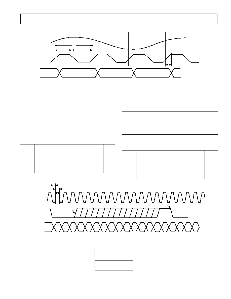
t
C
t
CL
t
CH
t
OD
DATA1
S4
S3
S2
S1
ANALOG
INPUT
INPUT
CLOCK
RXCLK
OUTPUT
DATA
RX11:RX0
Figure 4. Receive Interface Timing Diagram
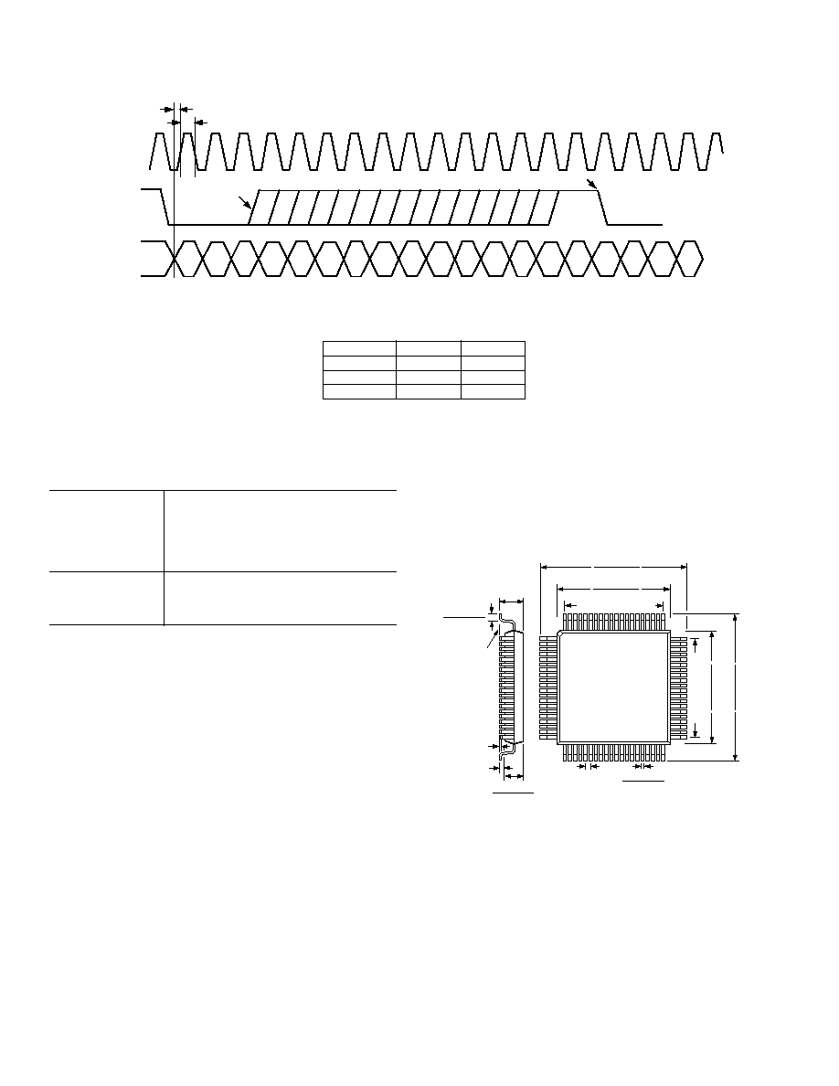
t
H
10ns
2
TX_CLK
TX_SYNC
TX_DATA
D11
MSB
D10
D9
D8
D7
D5
D6
D4
D3
D2
D1
D0
X
X
X
X
D11
MSB
D10
D9
1. THE RISING EDGE TO TX_SYNC CAN OCCUR ANYWHERE. TX_SYNC MUST BE AT LEAST ONE CLOCK CYCLE WIDE.
2. TX_SYNC FALLING EDGE MUST OCCUR AFTER THE TX_CLK RISING EDGE THAT CAPTURED THE SERIAL LSB.
THIS ENSURES CORRECT LOADING INTO THE DAC.
FULL SCALE
1/2 FULL SCALE
1/2 FULL SCALE
OUTPUT
MINUS 1LSB
ZERO
011111111111
000000000000
111111111111
WORD
100000000000
1
THE FIRST 12 BITS OF THE 16-BIT SERIAL WORD ARE THE INPUT TO THE TX PATH DAC, MSB FIRST. THE NUMBER
SYSTEM IS TWOS COMPLEMENT, AS FOLLOWS:
t
SU
12ns
Figure 5. Transmit Interface Timing Diagram
AD6472
8
REV. 0
C330284/98
PRINTED IN U.S.A.
80-Lead Metric Plastic Quad Flatpack
S-80A
SEATING
PLANE
0.134 (3.40)
MAX
0.041 (1.03)
0.029 (0.73)
0.004 (0.10)
MAX
0.120 (3.05)
0.100 (2.55)
0.010 (0.25)
MIN
0.015 (0.38)
0.009 (0.22)
0.690 (17.45)
0.667 (16.95)
0.555 (14.10)
0.547 (13.90)
0.555 (14.10)
0.547 (13.90)
0.690 (17.45
0.667 (16.95)
1
20
21
41
40
60
61
80
0.486 (12.35) BSC
0.486 (12.35) BSC
TOP VIEW
(PINS DOWN)
0.026 (0.65)
BSC
PCB Layout Recommendations
Analog and Digital
Separate the analog and digital grounds.
Ground Planes
Use a single 35 to 50 mil wide trace un-
der the device to connect the two ground
planes. Connect the IC ground pins
directly to the respective ground planes.
Power Supply
Use one 0.1
µ
F capacitor for each IC de-
Capacitors
coupling power supply connection in addi-
tion to capacitance shown in schematic.
OUTLINE DIMENSIONS
Dimensions shown in inches and (mm).
t
SU
12ns
t
H
10ns
2
SCLK
SFRAME
SDATA
D6
MSB
D5
D4
D3
D2
D0
D1
X
X
X
X
X
X
X
X
D6
MSB
D5
D4
1. THE RISING EDGE OF SFRAME CAN OCCUR ANYWHERE. SFRAME MUST BE AT LEAST ONE CLOCK CYCLE WIDE.
2. SFRAME FALLING EDGE MUST OCCUR BEFORE THE SCLK RISING EDGE THAT CAPTURED THE SERIAL LSB.
THIS ENSURES CORRECT LOADING INTO THE DAC.
FULL SCALE
MID-SCALE
MINIMUM
OUTPUT
1111111
1000000
0000000
WORD
VOLTAGE
4.5
2.5
0.5
1
THE FIRST 7 BITS OF THE 16-BIT SERIAL WORD ARE THE INPUT TO THE TR DAC, MSB FIRST. THE NUMBER
SYSTEM IS TWOS COMPLEMENT, AS FOLLOWS:
X
Figure 6. Timing Recovery DAC Converter Timing