REV. D
Information furnished by Analog Devices is believed to be accurate and
reliable. However, no responsibility is assumed by Analog Devices for its
use, nor for any infringements of patents or other rights of third parties that
may result from its use. No license is granted by implication or otherwise
under any patent or patent rights of Analog Devices.
a
Dual Precision,
Low Power BiFET Op Amp
AD648
FEATURES
DC Performance
400 A max Quiescent Current
10 pA max Bias Current, Warmed Up (AD648B)
1 V max Offset Voltage (AD648B)
10 V/ C max Drift (AD648B)
2 V p-p Noise, 0.1 Hz to 10 Hz
AC Performance
1.8 V/ s Slew Rate
1 MHz Unity Gain Bandwidth
Available in Plastic Mini-DIP, CERDIP, and Plastic SOIC
Packages
MIL-STD-883B Parts Available
Surface Mount (SOIC) Package Available in Tape and
Reel in Accordance with EIA-481A Standard
Single Version: AD548
PRODUCT DESCRIPTION
The AD648 is a matched pair of low power, precision mono-
lithic operational amplifiers. It offers both low bias current
(10 pA max, warmed up) and low quiescent current (400
µA
max) and is fabricated with ion-implanted FET and laser wafer
trimming technologies. Input bias current is guaranteed over the
AD648's entire common-mode voltage range.
The economical J grade has a maximum guaranteed offset
voltage of less than 2 mV and an offset voltage drift of less than
20
µV/°C. This level of dc precision is achieved using Analog's
laser wafer drift trimming process. The combination of low
quiescent current and low offset voltage drift minimizes changes
in input offset voltage due to self-heating effects. Five grades are
offered over the commercial, industrial and military temperature
ranges.
The AD648 is recommended for any dual supply op amp
application requiring low power and excellent dc and ac per-
formance. In applications such as battery-powered, precision
instrument front ends and CMOS DAC buffers, the AD648's
excellent combination of low input offset voltage and drift, low
bias current, and low 1/f noise reduces output errors. High
common-mode rejection (82 dB, min on the "B" grade) and
high open-loop gain ensures better than 12-bit linearity in high
impedance, buffer applications.
The AD648 is pinned out in a standard dual op amp configura-
tion and is available in seven performance grades. The AD648J
and AD648K are rated over the commercial temperature range
of 0
°C to 70°C. The AD648 and AD648B are rated over the
industrial temperature range of 40
°C to +85°C. The AD648S
and AD648T are rated over the military temperature range of
55
°C to +125°C and the AD648T* grade is available pro-
cessed to MIL-STD-883B, Rev. C.
The AD648 is available in an 8-lead plastic mini-DIP,
CERDIP, and SOIC.
*Not for new design, obsolete April 2002.
PRODUCT HIGHLIGHTS
1. A combination of low supply current, excellent dc and ac
performance and low drift makes the AD648 the ideal op
amp for high performance, low power applications.
2. The AD648 is pin compatible with industry standard dual
op amps such as the LF442, TL062, and AD642, enabling
designers to improve performance while achieving a reduc-
tion in power dissipation of up to 85%.
3. Guaranteed low input offset voltage (2 mV max) and drift
(20
µV/°C max) for the AD648J are achieved using Analog
Devices' laser drift trimming technology.
4. Analog Devices specifies each device in the warmed-up
condition, insuring that the device will meet its published
specifications in actual use.
5. Matching characteristics are excellent for all grades. The
input offset voltage matching between amplifiers in the
AD648J is within 2 mV.
6. Crosstalk between amplifiers is less than 120 dB at 1 kHz.
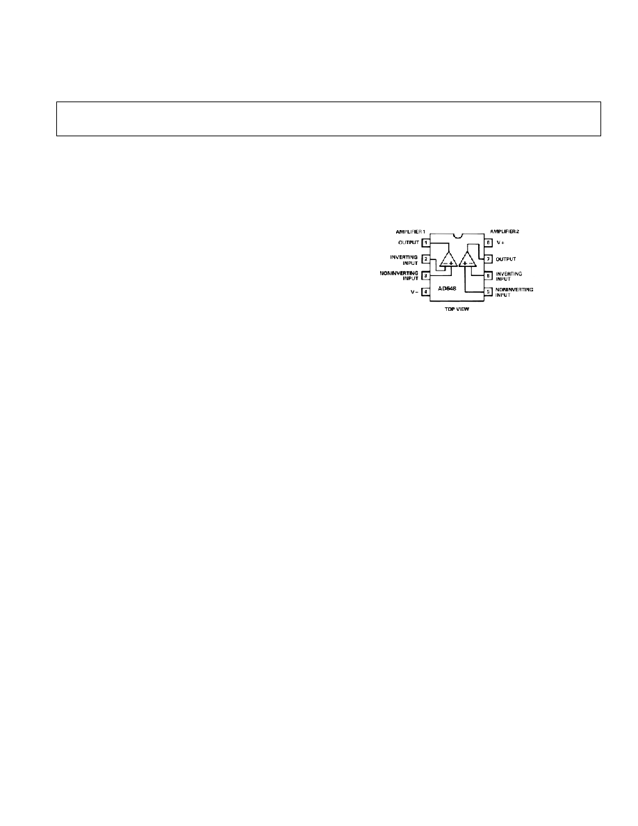
CONNECTION DIAGRAM
Plastic Mini-Dip (N) Package,
Plastic SOIC (R) Package
and
CERDIP (Q) Package
One Technology Way, P.O. Box 9106, Norwood, MA 02062-9106, U.S.A.
Tel: 781/329-4700
www.analog.com
Fax: 781/326-8703
© Analog Devices, Inc., 2002

AD648J/A/S
AD648K/B/T
Model
Min
Typ
Max
Min
Typ
Max
Unit
OUTPUT CHARACTERISTICS
Voltage @ R
L
10 k,
T
MIN
to T
MAX
±12/±12/±12
±13
±12
±13
V
Voltage @ R
L
5 k,
T
MIN
to T
MAX
±11/±11/±11
±12
±11
±12
V
Short Circuit Current
15
15
mA
POWER SUPPLY
Rated Performance
±15
±15
V
Operating Range
±4.5
±18
±4.5
±18
V
Quiescent Current (Both Amplifiers)
340
400
340
400
µA
TEMPERATURE RANGE
Operating, Rated Performance
Commercial (0
°C to 70°C)
AD648J
AD648K
Industrial (40
°C to +85°C)
AD648A
AD648B
Military (55
°C to +125°C)
AD648S
AD648T
PACKAGE OPTIONS
SOIC (R-8)
AD648JR
AD648KR
Plastic (N-8)
AD648JN
AD648KN
CERDIP (Q-8)
AD648AQ
5
, AD648SQ
5
AD648BQ
5
, AD648TQ/883B
5
Tape and Reel
AD648JR-REEL, AD648JR-REEL7 AD648KR-REEL, AD648KR-REEL7
NOTES
1
Input Offset Voltage specifications are guaranteed after five minutes of operation at T
A
= 25
°C.
2
Bias Current specifications are guaranteed maximum at either input after five minutes of operation at T
A
= 25
°C. For higher temperature, the current doubles
every 10
°C.
3
Matching is defined as the difference between parameters of the two amplifiers.
4
Defined as voltages between inputs, such that neither exceeds
± 10 V from ground.
5
Not for new design. Obsolete April 2002.
Specifications subject to change without notice.
AD648
REV. D
3
SPECIFICATIONS
(Continued)
AD648
REV. D
4
WARNING!
ESD SENSITIVE DEVICE
CAUTION
ESD (electrostatic discharge) sensitive device. Electrostatic charges as high as 4000 V readily
accumulate on the human body and test equipment and can discharge without detection.
Although the AD648 features proprietary ESD protection circuitry, permanent damage may
occur on devices subjected to high-energy electrostatic discharges. Therefore, proper ESD
precautions are recommended to avoid performance degradation or loss of functionality.
ABSOLUTE MAXIMUM RATINGS
1
Supply Voltage . . . . . . . . . . . . . . . . . . . . . . . . . . . . . . . . .
±18 V
Internal Power Dissipation
2
. . . . . . . . . . . . . . . . . . . . 500 mW
Input Voltage
3
. . . . . . . . . . . . . . . . . . . . . . . . . . . . . . . .
±18 V
Output Short Circuit Duration . . . . . . . . . . . . . . . . . Indefinite
Differential Input Voltage . . . . . . . . . . . . . . . . . . +V
S
and V
S
Storage Temperature Range (Q, H) . . . . . . . 65
°C to +150°C
Storage Temperature Range
(N, R) . . . . . . . . 65
°C to +125°C
Operating Temperature Range
AD648J/K . . . . . . . . . . . . . . . . . . . . . . . . . . . . . 0
°C to 70°C
AD648A/B . . . . . . . . . . . . . . . . . . . . . . . . . . 40
°C to +85°C
AD648S/T . . . . . . . . . . . . . . . . . . . . . . . . . 55
°C to +125°C
Lead Temperature Range (Soldering 60 sec) . . . . . . . . . 300
°C
NOTES
1
Stresses above those listed under "Absolute Maximum Ratings" may cause
permanent damage to the device. This is a stress rating only and functional
operation of the device at these or any other conditions above those indicated in
the operational section of this specification is not implied. Exposure to absolute
maximum rating conditions for extended periods may affect device reliability.
2
Thermal Characteristics:
8-Pin Plastic Package:
JA
= 165
°C/Watt
8-Pin CERDIP Package:
JC
= 22
°C/Watt;
JA
= 110
°C/Watt
8-Pin SOIC Package:
JC
= 42
°C/Wat;
JA
= 160
°C/Watt
3
For supply voltages less than
± 18 V, the absolute maximum input voltage is equal
to the supply voltage.