/home/web/htmldatasheet/RUSSIAN/html/ad/164251
REV. A
Information furnished by Analog Devices is believed to be accurate and
reliable. However, no responsibility is assumed by Analog Devices for its
use, nor for any infringements of patents or other rights of third parties that
may result from its use. No license is granted by implication or otherwise
under any patent or patent rights of Analog Devices.
a
AD6620
One Technology Way, P.O. Box 9106, Norwood, MA 02062-9106, U.S.A.
Tel: 781/329-4700
www.analog.com
Fax: 781/326-8703
© Analog Devices, Inc., 2001
67 MSPS Digital Receive
Signal Processor
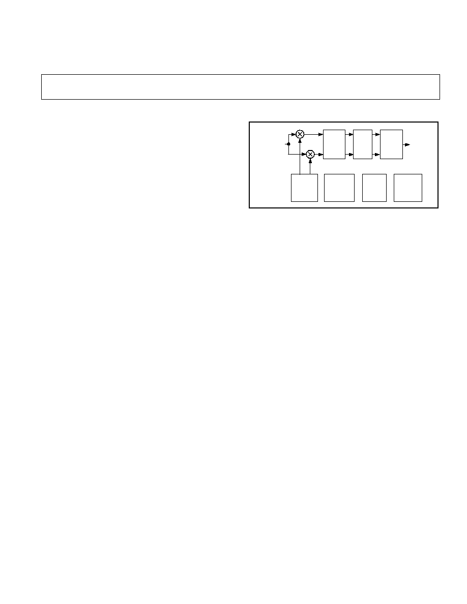
FUNCTIONAL BLOCK DIAGRAM
REAL,
DUAL REAL,
OR COMPLEX
INPUTS
SERIAL OR
PARALLEL
OUTPUTS
CIC
FILTERS
OUTPUT
FORMAT
COMPLEX
NCO
P
OR SERIAL
CONTROL
I
Q
SIN
COS
EXTERNAL
SYNC
CIRCUITRY
JTAG
PORT
I
I
Q
Q
FIR
FILTER
AD6620
FEATURES
High Input Sample Rate
67 MSPS Single Channel Real
33.5 MSPS Diversity Channel Real
33.5 MSPS Single Channel Complex
NCO Frequency Translation
Worst Spur Better than 100 dBc
Tuning Resolution Better than 0.02 Hz
2nd Order Cascaded Integrator Comb FIR Filter
Linear Phase, Fixed Coefficients
Programmable Decimation Rates: 2, 3 . . . 16
5th Order Cascaded Integrator Comb FIR Filter
Linear Phase, Fixed Coefficients
Programmable Decimation Rates: 1, 2, 3 . . . 32
Programmable Decimating RAM Coefficient FIR Filter
Up to 134 Million Taps per Second
256 20-Bit Programmable Coefficients
Programmable Decimation Rates: 1, 2, 3 . . . 32
Bidirectional Synchronization Circuitry
Phase Aligns NCOs
Synchronizes Data Output Clocks
Serial or Parallel Baseband Outputs
Pin Selectable Serial or Parallel
Serial Works with SHARC
®
, ADSP-21xx, Most Other
DSPs
16-Bit Parallel Port, Interleaved I and Q Outputs
Two Separate Control and Configuration Ports
Generic P Port, Serial Port
3.3 V Optimized CMOS Process
JTAG Boundary Scan
GENERAL DESCRIPTION
The AD6620 is a digital receiver with four cascaded signal-
processing elements: a frequency translator, two fixed-
coefficient decimating filters, and a programmable coefficient
decimating filter. All inputs are 3.3 V LVCMOS compatible.
All outputs are LVCMOS and 5 V TTL compatible.
As ADCs achieve higher sampling rates and dynamic range, it
becomes increasingly attractive to accomplish the final IF stage
of a receiver in the digital domain. Digital IF Processing is less
expensive, easier to manufacture, more accurate, and more
flexible than a comparable highly selective analog stage.
The AD6620 diversity channel decimating receiver is designed
to bridge the gap between high-speed ADCs and general pur-
pose DSPs. The high resolution NCO allows a single carrier to
be selected from a high speed data stream. High dynamic range
decimation filters with a wide range of decimation rates allow
both narrowband and wideband carriers to be extracted. The
RAM-based architecture allows easy reconfiguration for multi-
mode applications.
The decimating filters remove unwanted signals and noise from
the channel of interest. When the channel of interest occupies
less bandwidth than the input signal, this rejection of out-of-
band noise is called "processing gain." By using large decimation
factors, this "processing gain" can improve the SNR of the
ADC by 36 dB or more. In addition, the programmable RAM
Coefficient filter allows antialiasing, matched filtering, and
static equalization functions to be combined in a single, cost-
effective filter.
The input port accepts a 16-bit Mantissa, a 3-bit Exponent,
and an A/B Select pin. These allow direct interfacing with the
AD6600, AD6640, AD6644, AD9042 and most other high-
speed ADCs. Three input modes are provided: Single Channel
Real, Single Channel Complex, and Diversity Channel Real.
When paired with an interleaved sampler such as the AD6600,
the AD6620 can process two data streams in the Diversity
Channel Real input mode. Each channel is processed with coher-
ent frequency translation and output sample clocks. In addition,
external synchronization pins are provided to facilitate coherent
frequency translation and output sample clocks among several
AD6620s. These features can ease the design of systems with
diversity antennas or antenna arrays.
Units are packaged in an 80-lead PQFP (plastic quad flatpack)
and specified to operate over the industrial temperature range
(40
°C to +85°C).
SHARC is a registered trademark of Analog Devices, Inc.
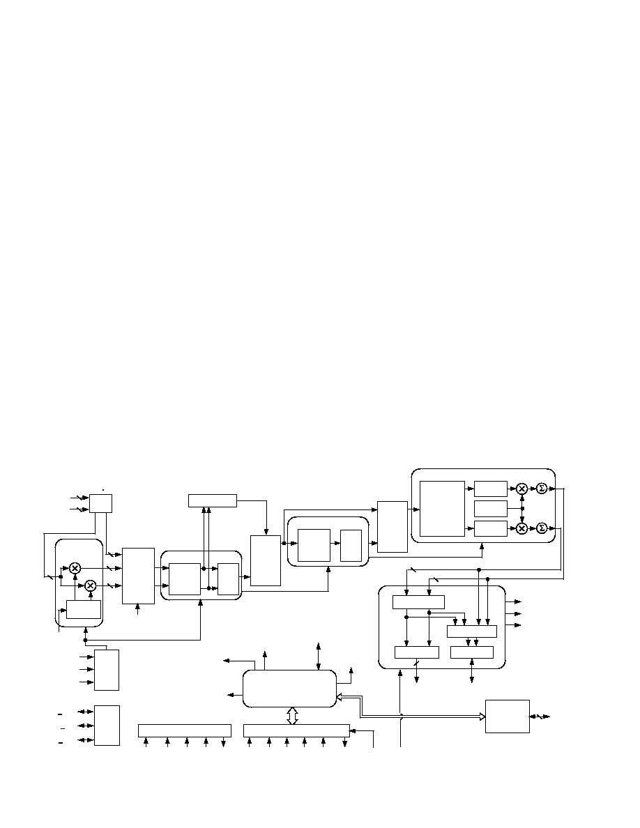
AD6620
2
REV. A
I-RAM
256 18
C-RAM
256 20
Q-RAM
256 18
M
RCF
RCF
M
CICS
CIC5
SCALING
INTERLEAVE
DE-
INTERLEAVE
MULTI-
PLEXER
M
CICS
CIC2
SCALING
MULTI-
PLEXER
EXP
SCALING
FREQUENCY
TRANSLATOR
3
18
18
I
Q
16
INPUT
DATA
3
EXP[2:0]
16
IN[15:0]
COMPLEX
NCO
f
SAMP5
EXPLNV,
EXPOFF
TIMING
SYNC
I/O
CLK
A/B
RESET
SYNC RCF
SYNC CIC
SYNC NCO
PHASE
OFFSET
f
SAMP2
f
SAMP
MULTIPLEXER
SCALING, S
OUT
SERIAL
PARALLEL
16
23
23
DV
OUT
I/Q
OUT
A/B
OUT
PARALLEL
OUTPUTS
AND
SERIAL I/O
16
OUT[15:0]
SCLK
SDI
SDO
SDFS
SDFE
SBM
WL[1:0]
AD
SDIV[3:0]
RCF COEFFICIENTS
NUMBER OF TAPS
DECIMATE FACTOR
ADDRESS OFFSET
CIC2, CIC5
DECIMATE FACTORS
SCALE FACTORS
NCO FREQUENCY
PHASE OFFSET
DITHER
SYNC MASK
INPUT MODE
REAL, DUAL, COMPLEX
FIXED OR WITH EXPONENT
SYNC M/S
OUTPUT
SCALE
FACTOR
JTAG
TRST
TCK
TMS
TDI
TDO
MICROPROCESSOR INTERFACE
DS
D[7:0] A[2:0]
R/W
DTACK
CS
MODE PAR/SER
CONTROL REGISTERS
MICROPORT AND
SERIAL ACCESS
(
W/R)
(RDY)
(
R/D)
OUTPUT
Figure 1. Block Diagram
TABLE OF CONTENTS
GENERAL DESCRIPTION . . . . . . . . . . . . . . . . . . . . . . . . . 1
ARCHITECTURE . . . . . . . . . . . . . . . . . . . . . . . . . . . . . . . . 2
SPECIFICATIONS . . . . . . . . . . . . . . . . . . . . . . . . . . . . . . . 4
TIMING . . . . . . . . . . . . . . . . . . . . . . . . . . . . . . . . . . . . . . . . 5
ABSOLUTE MAXIMUM RATINGS . . . . . . . . . . . . . . . . 11
EXPLANATION OF TEST LEVELS . . . . . . . . . . . . . . . . 11
ORDERING GUIDE . . . . . . . . . . . . . . . . . . . . . . . . . . . . . 11
PIN FUNCTION DESCRIPTIONS . . . . . . . . . . . . . . . . . 12
PIN CONFIGURATIONS . . . . . . . . . . . . . . . . . . . . . . . . . 13
INPUT DATA PORT . . . . . . . . . . . . . . . . . . . . . . . . . . . . . 15
OUTPUT DATA PORT . . . . . . . . . . . . . . . . . . . . . . . . . . . 18
FREQUENCY TRANSLATOR . . . . . . . . . . . . . . . . . . . . . 19
SECOND ORDER CASCADED INTEGRATOR
COMB FILTER . . . . . . . . . . . . . . . . . . . . . . . . . . . . . . . 21
FIFTH ORDER CASCADED INTEGRATOR
COMB FILTER . . . . . . . . . . . . . . . . . . . . . . . . . . . . . . . 23
RAM COEFFICIENT FILTER . . . . . . . . . . . . . . . . . . . . . 25
CONTROL REGISTERS AND ON-CHIP RAM . . . . . . . 27
PROGRAMMING THE AD6620 . . . . . . . . . . . . . . . . . . . 30
ACCESS PROTOCOLS . . . . . . . . . . . . . . . . . . . . . . . . . . . 31
MICROPORT CONTROL . . . . . . . . . . . . . . . . . . . . . . . . 32
SERIAL PORT CONTROL . . . . . . . . . . . . . . . . . . . . . . . . 35
JTAG BOUNDARY SCAN . . . . . . . . . . . . . . . . . . . . . . . . 37
APPLICATIONS . . . . . . . . . . . . . . . . . . . . . . . . . . . . . . . . 38
OUTLINE DIMENSIONS . . . . . . . . . . . . . . . . . . . . . . . . . 44
ARCHITECTURE
As shown in Figure 1, the AD6620 has four main signal pro-
cessing stages: a Frequency Translator, two Cascaded Integrator
Comb FIR Filters (CIC2, CIC5), and a RAM Coefficient FIR
Filter (RCF). Multiple modes are supported for clocking data
into and out of the chip. Programming and control is accom-
plished via serial and microprocessor interfaces.
Input data to the chip may be real or complex. If the input data
is real, it may be clocked in as a single channel or interleaved
with a second channel. The two-channel input mode, called
Diversity Channel Real, is typically used in diversity receiver
applications. Input data is clocked in 16-bit parallel words,
IN[15:0]. This word may be combined with exponent input bits
EXP[2:0] when the AD6620 is being driven by floating-point or
gain-ranging analog-to-digital converters such as the AD6600.
Frequency translation is accomplished with a 32-bit complex
Numerically Controlled Oscillator (NCO). Real data entering
this stage is separated into in-phase (I) and quadrature (Q)
components. This stage translates the input signal from a digital
intermediate frequency (IF) to baseband. Phase and amplitude
dither may be enabled on-chip to improve spurious performance
of the NCO. A phase offset word is available to create a known
phase relationship between multiple AD6620s.
Following frequency translation is a fixed coefficient, high speed
decimating filter that reduces the sample rate by a program-
mable ratio between 2 and 16. This is a second order, cascaded
integrator comb FIR filter shown as CIC2 in Figure 1. (Note:
Decimation of 1 in CIC2 requires 2
× or greater clock into
AD6620). The data rate into this stage equals the input data
rate, f
SAMP
. The data rate out of CIC2, f
SAMP2
, is determined by
the decimation factor, M
CIC2
.
AD6620
3
REV. A
Following CIC2 is the second fixed-coefficient decimating filter.
This filter, CIC5, further reduces the sample rate by a program-
mable ratio from 1 to 32. The data rate out of CIC5, f
SAMP5
, is
determined by the decimation factors of M
CIC5
and M
CIC2
.
Each CIC stage is a FIR filter whose response is defined by the
decimation rate. The purpose of these filters is to reduce the
data rate of the incoming signal so that the final filter stage, a FIR
RAM coefficient sum-of-products filter (RCF), can calculate
more taps per output. As shown in Figure 1, on-chip multiplex-
ers allow both CIC filters to be bypassed if a multirate clock
is used.
The fourth stage is a sum-of-products FIR filter with program-
mable 20-bit coefficients, and decimation rates programmable
from 1 to 32. The RAM Coefficient FIR Filter (RCF in Figure
1) can handle a maximum of 256 taps.
The overall filter response for the AD6620 is the composite of
all three cascaded decimating filters: CIC2, CIC5, and RCF. Each
successive filter stage is capable of narrower transition band-
widths but requires a greater number of CLK cycles to calculate
the output. More decimation in the first filter stage will minimize
overall power consumption. Data comes out via a parallel port
or a serial interface.
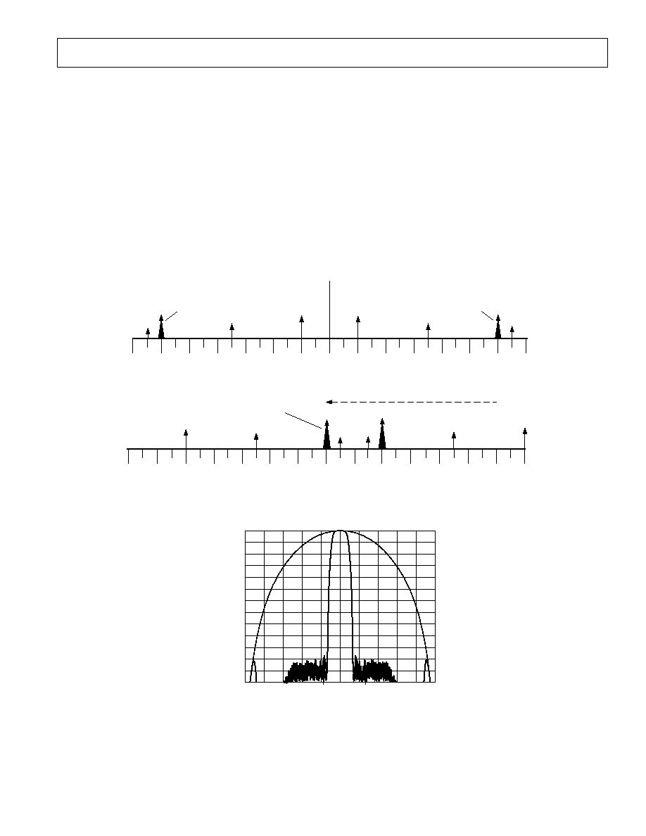
Figure 2 illustrates the basic function of the AD6620: to select
and filter a single channel from a wide input spectrum. The
frequency translator "tunes" the desired carrier to baseband.
CIC2 and CIC5 have fixed order responses; the RCF filter
provides the sharp transitions. More detail is provided in later
sections of the data sheet.
f
S
/2
3f
S
/8
5f
S
/16
f
S
/4
3f
S
/16
f
S
/8
f
S
/16
DC
f
S
/16
f
S
/8
3f
S
/16
f
S
/4
5f
S
/16
f
S
/2
3f
S
/8
SIGNAL OF
INTEREST
SIGNAL OF INTEREST "IMAGE"
WIDEBAND INPUT SPECTRUM
(f
samp/
2 TO f
samp/
2)
D'
C'
B'
A'
A
C
B
D
Figure 2a. Wideband Input Spectrum (e.g., 30 MHz from High-Speed ADC)
f
S
/2
3f
S
/8
5f
S
/16
f
S
/4
3f
S
/16
f
S
/8
f
S
/16
DC
f
S
/16
f
S
/8
3f
S
/16
f
S
/4
5f
S
/16
f
S
/2
3f
S
/8
AFTER FREQUENCY TRANSLATION
NCO "TUNES" SIGNAL TO BASEBAND
A
B
C
D
D'
C'
B'
A'
Figure 2b. Frequency Translation (e.g., Single 1 MHz Channel Tuned to Baseband)
0
10
20
30
40
50
60
70
80
90
100
110
120
130
CIC2, CIC5, AND RCF
dBc
FREQUENCY
Figure 2c. Baseband Signal is Decimated and Filtered by CIC2, CIC5, RCF

4
REV. A
AD6620SPECIFICATIONS
RECOMMENDED OPERATING CONDITIONS
Test
AD6620AS
Parameter
Level
Min
Typ
Max
Unit
VDD
I
3.0
3.3
3.6
V
T
AMBIENT
IV
40
+25
+85
°C
ELECTRICAL CHARACTERISTICS
Test
AD6620AS
Parameter (Conditions)
Temp
Level
Min
Typ
Max
Unit
LOGIC INPUTS
1, 2, 3, 4, 5, 6, 7
(NOT 5 V TOLERANT)
Logic Compatibility
Full
3.3 V CMOS
Logic "1" Voltage
Full
I
2.0
VDD + 0.3
V
Logic "0" Voltage
Full
I
0.3
0.8
V
Logic "1" Current
Full
I
1
10
µA
Logic "0" Current
Full
I
1
10
µA
Input Capacitance
25
°C
V
4
pF
LOGIC OUTPUTS
2, 4, 7, 8, 9, 10, 11
Logic Compatibility
Full
3.3 V CMOS/TTL
Logic "1" Voltage (I
OH
= 0.5 mA)
Full
I
2.4
VDD 0.2
V
Logic "0" Voltage (I
OL
= 1.0 mA)
Full
I
0.2
0.4
V
IDD SUPPLY CURRENT
CLK = 20 MHz
12
Full
V
52
mA
CLK = 65 MHz
13
Full
I
167
227
mA
Reset Mode
14
Full
I
1
mA
POWER DISSIPATION
CLK = 20 MHz
12
Full
V
170
mW
CLK = 65 MHz
13
Full
I
550
750
mW
Reset Mode
14
Full
I
3.3
mW
NOTES
1
Input-Only Pins: CLK,
RESET, IN[15:0], EXP[2:0], A/B, PAR/SEL.
2
Bidirectional Pins: SYNC_NCO, SYNC_CIC, SYNC_RCF.
3
Microinterface Input Pins:
DS (RD), R/W (WR), CS.
4
Microinterface Bidirectional Pins: A[2:0], D[7:0].
5
JTAG Input Pins:
TRST, TCK, TMS, TDI.
6
Serial Mode Input Pins: SDI, SBM, WL[1:0], AD, SDIV[3:0].
7
Serial Mode Bidirectional Pins: SCLK, SDFS.
8
Output Pins: OUT[15:0], DV
OUT
, A/B
OUT
, I/Q
OUT
.
9
Microinterface Output Pins:
DTACK (RDY).
10
JTAG Output Pins: TDO.
11
Serial Mode Output Pins: SDO, SDFE.
12
Conditions for IDD @ 20 MHz. M
CIC2
= 2, M
CIC5
= 2, M
RCF
= 1, 4 RCF taps of alternating positive and negative full scale.
13
Conditions for IDD @ 65 MHz. M
CIC2
= 2, M
CIC5
= 2, M
RCF
= 1, 4 RCF taps of alternating positive and negative full scale.
14
Conditions for IDD in Reset (
RESET = 0).
Specifications subject to change without notice.

5
REV. A
AD6620
TIMING CHARACTERISTICS
(C
LOAD
= 40 pF All Outputs)
Test
AD6620AS
Parameter (Conditions)
Temp
Level
Min
Typ
Max
Unit
CLK Timing Requirements:
t
CLK
CLK Period
Full
I
14.93
1
ns
t
CLK
CLK Period
Full
I
15.4
ns
t
CLKL
CLK Width Low
Full
IV
7.0
0.5
× t
CLK
ns
t
CLKH
CLK Width High
Full
IV
7.0
0.5
× t
CLK
ns
Reset Timing Requirements:
t
RESL
RESET Width Low
Full
I
30.0
ns
Input Data Timing Requirements:
t
SI
Input
2
to CLK Setup Time
Full
IV
1.0
ns
t
HI
Input
2
to CLK Hold Time
Full
IV
6.5
ns
Parallel Output Switching Characteristics:
t
DPR
CLK to OUT[15:0] Rise Delay
Full
IV
8.0
19.5
ns
t
DPF
CLK to OUT[15:0] Fall Delay
Full
IV
7.5
19.5
ns
t
DPR
CLK to DV
OUT
Rise Delay
Full
IV
6.5
19.0
ns
t
DPF
CLK to DV
OUT
Fall Delay
Full
IV
5.5
11.5
ns
t
DPR
CLK to IQ
OUT
Rise Delay
Full
IV
7.0
19.5
ns
t
DPF
CLK to IQ
OUT
Fall Delay
Full
IV
6.0
13.5
ns
t
DPR
CLK to AB
OUT
Rise Delay
Full
IV
7.0
19.5
ns
t
DPF
CLK to AB
OUT
Fall Delay
Full
IV
5.5
13.5
ns
SYNC Timing Requirements:
t
SY
SYNC
3
to CLK Setup Time
Full
IV
1.0
ns
t
HY
SYNC
3
to CLK Hold Time
Full
IV
6.5
ns
SYNC Switching Characteristics:
t
DY
CLK to SYNC
4
Delay Time
Full
V
7.0
23.5
ns
Serial Input Timing:
t
SSI
SDI to SCLK
t Setup Time
Full
IV
1.0
ns
t
HSI
SDI to SCLK
t Hold Time
Full
IV
2.0
ns
t
HSRF
SDFS to SCLK
u Hold Time
Full
IV
4.0
ns
t
SSF
SDFS to SCLK
t Setup Time
5
Full
IV
1.0
ns
t
HSF
SDFS to SCLK
t Hold Time
5
Full
IV
2.0
ns
Serial Frame Output Timing:
t
DSE
SCLK
u to SDFE Delay Time
Full
IV
3.5
11.0
ns
t
SDFEH
SDFE Width High
Full
V
t
SCLK
ns
t
DSO
SCLK
u to SDO Delay Time
Full
IV
4.5
11.0
ns
SCLK Switching Characteristics, SBM = "1":
t
SCLK
SCLK Period
4
Full
I
2
× t
CLK
ns
t
SCLKL
SCLK Width Low
Full
V
0.5
× t
SCLK
ns
t
SCLKH
SCLK Width High
Full
V
0.5
× t
SCLK
ns
t
SCLKD
CLK to SCLK Delay Time
Full
V
6.5
13.0
ns
Serial Frame Timing, SBM = "1":
t
DSF
SCLK
u to SDFS Delay Time
Full
IV
1.0
4.0
ns
t
SDFSH
SDFS Width High
Full
V
t
SCLK
ns
SCLK Timing Requirements, SBM = "0":
t
SCLK
SCLK Period
Full
I
15.4
ns
t
SCLKL
SCLK Width Low
Full
IV
0.4
× t
SCLK
0.5
× t
SCLK
ns
t
SCLKH
SCLK Width High
Full
IV
0.4
× t
SCLK
0.5
× t
SCLK
ns
NOTES
1
This specification valid for VDD >= 3.3 V. t
CLKL
and t
CLKH
still apply.
2
Specification pertains to: IN[15:0], EXP[2:0], A/B.
3
Specification pertains to: SYNC_NCO, SYNC_CIC, SYNC_RCF.
4
SCLK period will be
2 × t
CLK
when AD6620 is Serial Bus Master (SBM = 1) depending on the SDIV word.
5
SDFS setup and hold time must be met, even when configured as outputs, since internally the signal is sampled at the pad.
Specifications subject to change without notice.

AD6620
6
REV. A
TIMING CHARACTERISTICS
(C
LOAD
= 40 pF All Outputs)
Test
AD6620AS
Parameter (Conditions)
Temp
Level
Min
Typ
Max
Unit
MICROPROCESSOR PORT, MODE = 0
MODE0 Input Timing Requirements:
t
SC
Control
1
to CLK Setup Time
Full
IV
3.0
ns
t
HC
Control
1
to CLK Hold Time
Full
IV
5.0
ns
t
HA
Address
2
to CLK Hold Time
Full
IV
3.0
ns
t
ZR
CS to Data Enabled Time
Full
IV
5.0
ns
t
ZD
CS to Data Disabled Time
Full
IV
5.0
ns
t
SAM
CS to Address/Data Setup Time
Full
IV
0.0
ns
MODE0 Read Switching Characteristics:
t
DD
CLK to Data Valid Time
Full
I
10.0
15.0
30.0
ns
t
RDY
RD to RDY Time
Full
IV
4.0
19.5
ns
MODE0 Write Timing Requirements:
t
SC
Control
1
to CLK Setup Time
Full
IV
3.0
ns
t
HC
Control
1
to CLK Hold Time
Full
IV
5.0
ns
t
HM
Micro Data
3
to CLK Hold Time
Full
IV
3.0
ns
t
HA
Address
2
to CLK Hold Time
Full
IV
3.0
ns
t
SAM
Address/Data Setup Time to
CS
Full
IV
0.0
ns
MODE0 Write Switching Characteristics:
t
RDY
RD to RDY Time
Full
IV
4.0
19.5
ns
MICROPROCESSOR PORT, MODE = 1
MODE1 Input Timing Requirements:
t
SC
Control
1
to CLK Setup Time
Full
IV
3.0
ns
t
HC
Control
1
to CLK Hold Time
Full
IV
5.0
ns
t
HA
Address
2
to CLK Hold Time
Full
IV
3.0
ns
t
ZR
CS to Data Enabled Time
Full
IV
5.0
ns
t
ZD
CS to Data Disabled Time
Full
IV
5.0
ns
t
SAM
Address/Data Setup Time to
CS
Full
IV
0.0
ns
MODE1 Read Switching Characteristics:
t
DD
CLK to Data Valid Time
Full
I
10.0
30.0
ns
t
DTACK
CLK to DTACK Time
Full
V
5.5
15.5
ns
MODE1 Write Timing Requirements:
t
SC
Control
1
to CLK Setup Time
Full
IV
0.0
ns
t
HC
Control
1
to CLK Hold Time
Full
IV
5.0
ns
t
HM
Micro Data
3
to CLK Hold Time
Full
IV
6.5
ns
t
HA
Address
2
to CLK Hold Time
Full
IV
3.0
ns
t
SAM
Address/Data Setup Time to
CS
Full
IV
0.0
ns
MODE1 Write Switching Characteristic:
t
DTACK
CLK to DTACK Time
Full
V
5.5
15.5
ns
NOTES
1
Specification pertains to: R/W (
WR), DS (RD), CS.
2
Specification pertains to: A[2:0].
3
Specification pertains to: D[7:0].
Specifications subject to change without notice.
AD6620
7
REV. A
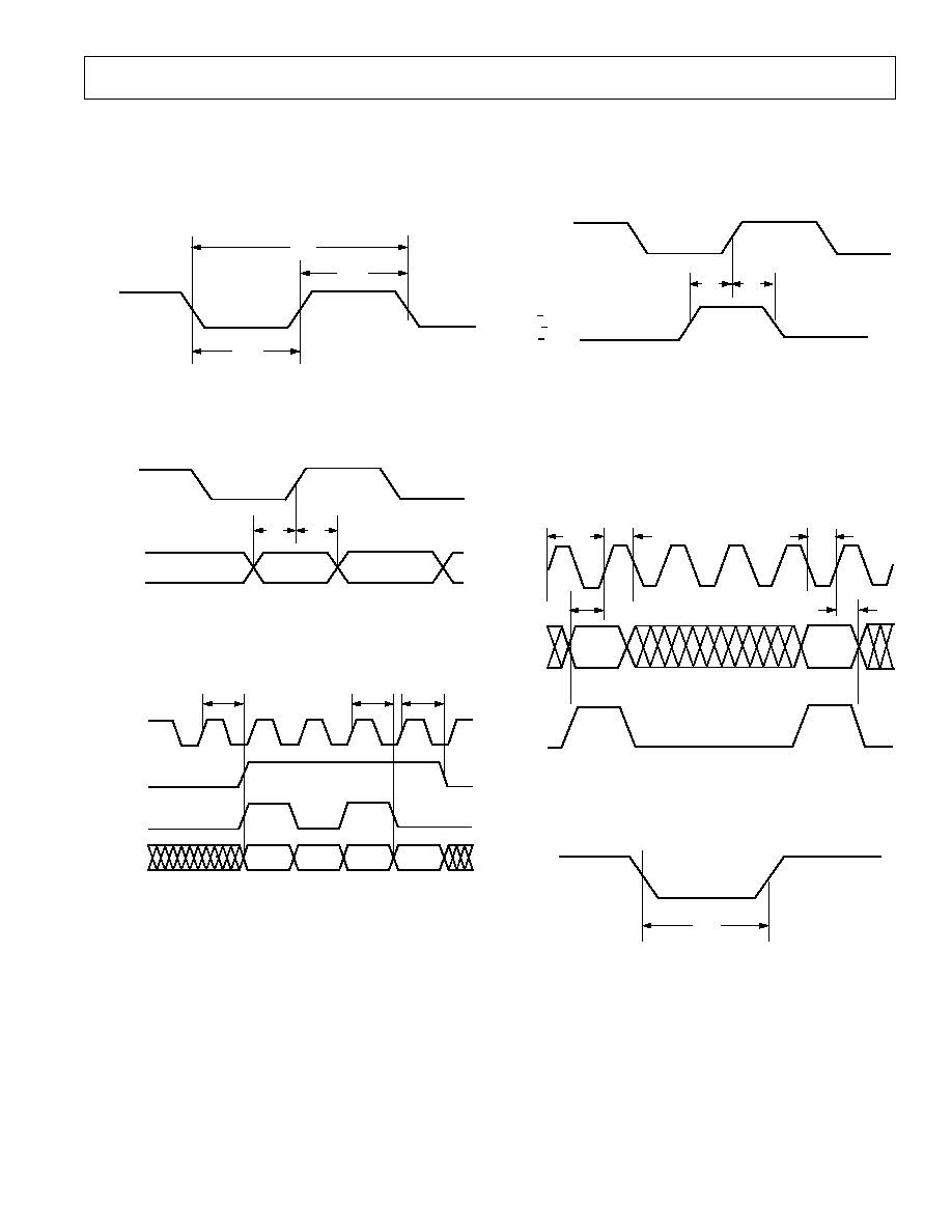
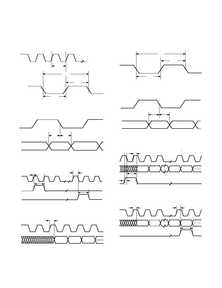
TIMING DIAGRAMS
CLK, INPUTS, PARALLEL OUTPUTS
RESET with PAR/SER = "1" establishes Parallel Outputs active.
t
CLKH
t
CLKL
t
CLK
CLK
Figure 3. CLK Timing Requirements
CLK
IN[15:0]
EXP[2:0]
A/B
t
SI
t
HI
DATA
Figure 4. Input Data Timing Requirements
CLK
OUT[15:0]
VALID OUTPUT DATA
DV
OUT
I/Q
OUT
t
DPR
t
DPF
I
Q
I
Q
I
A
Q
A
I
B
Q
B
t
DPF
Figure 5. Parallel Output Switching Characteristics
SYNC PULSES: SLAVE OR MASTER
t
SY
t
HY
CLK
SYNC NCO
SYNC CIC
SYNC RCF
NOTE:
IN THE SLAVE MODE WITH SINGLE CHANNEL OPERATION, THE WIDTH
OF THE SYNC_NCO SHOULD BE ONE SAMPLE CLOCK CYCLE. IN DUAL
CHANNEL MODE, THE PULSEWIDTH SHOULD BE TWO SAMPLE CLOCK
CYCLES. IF A PULSE LONGER THAN SPECIFIED IS USED, THE NCO WILL
BE INHIBITED AND NOT INCREMENT PROPERLY.
Figure 6. SYNC Slave Timing Requirements
CLK
t
CHP
t
CPL
t
CS
t
CH
IN[15:0]
E[2:0]
A/B
N+1
N
t
CLK
Figure 7. SYNC Master Delay
t
RESL
RESET
Figure 8. Reset Timing Requirements
AD6620
8
REV. A
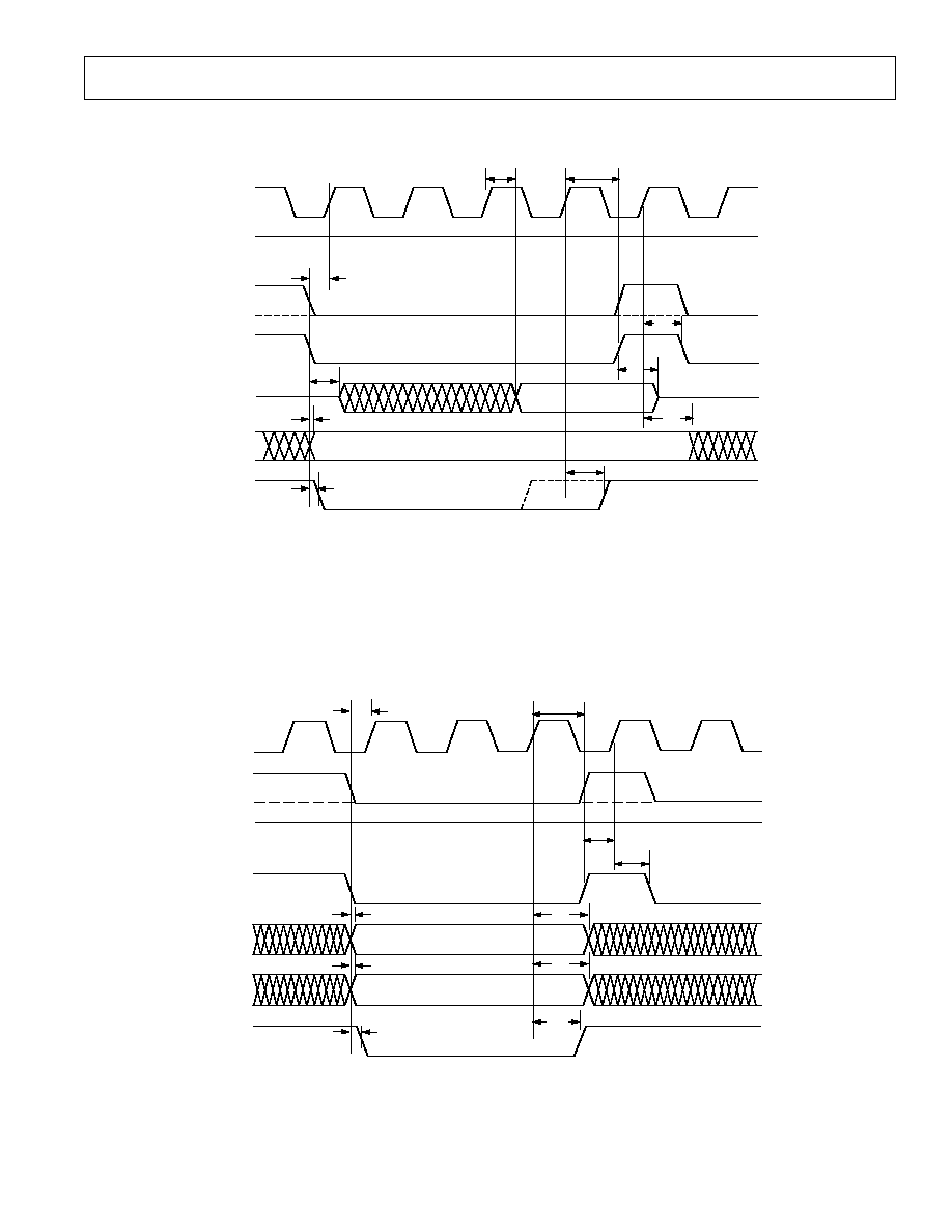
SERIAL PORT: BUS MASTER
RESET with PAR/SER = "0" establishes Serial Port active.
SBM = "1" puts AD6620 in Serial Bus Master mode SCLK is
output; SDFS is output.
t
SCLKD
t
SCLKL
t
SCLKH
CLK
SCLK
t
SCLK
Figure 9. SCLK Switching Characteristics
t
SSI
t
HSI
DATA
SDI
SCLK
Figure 10. Serial Input Data Timing Requirements
SCLK
t
DSF
t
DSE
t
SDFEH
t
SDFSH
SDFS
SDFE
Figure 11. Serial Frame Switching Characteristics
t
DSO
I
15
I
14
I
13
SCLK
SDO
Figure 12. Serial Output Data Switching Characteristics
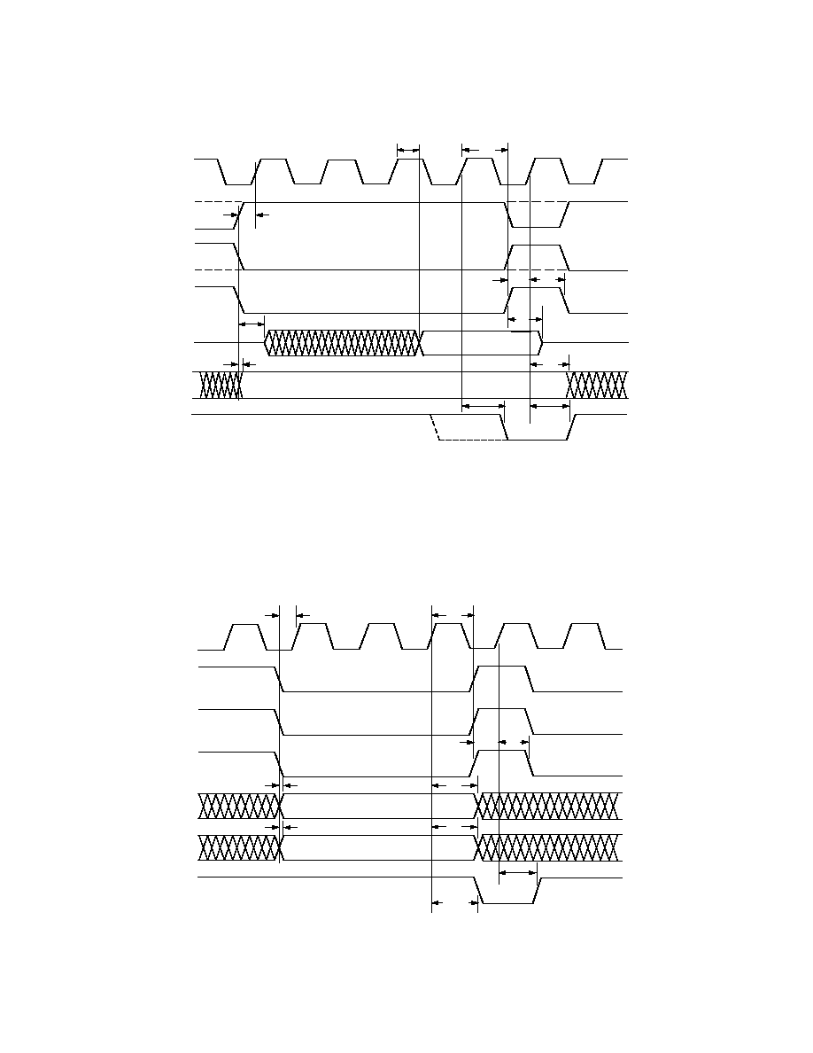
SERIAL PORT: CASCADE MODE
RESET with PAR/SER = "0" establishes Serial Port active.
SBM = "0" puts AD6620 in Serial Port Cascade mode, SCLK
is input; SDFS is input.
t
SCLK
t
SCLKH
t
SCLKL
SCLK
Figure 13. SCLK Timing Requirements
t
SSI
t
HSI
SCLK
SDI
DATA
Figure 14. Serial Input Data Timing Requirements
t
HSRF
I
15
I
14
SCLK
SDO
t
HSF
Q
1
Q
0
SDFS
t
SSF
Figure 15. SDO/SDFS Timing Requirements
t
DSO
I
15
I
14
SCLK
SDO
t
DSE
t
SDFEH
Q
1
Q
0
SDFE
Figure 16. SDO, SDFE Switching Characteristics
AD6620
9
REV. A
MICROPORT MODE0, READ
Timing is synchronous to CLK; MODE = 0.
t
DD
DATA VALID
t
HC
t
SC
t
HC
t
ZD
t
HA
t
RDY
t
RDY
ADDRESS VALID
t
SAM
t
ZR
N
N+1
N+2
N+3
N+4
N
CLK
1
WR
2
RD
2
CS
3
D[7:0]
RDY
1
A[2:0]
NOTES:
1
RDY IS DRIVEN LOW ASYNCHRONOUSLY BY
RD AND CS GOING LOW AND RETURNS HIGH ON THE RISING EDGE
OF CLK "N+3" FOR INTERNAL ACCESS (A[2:0] = 000), CLK "N+2" OTHERWISE.
2
THE SIGNAL,
WR, MAY REMAIN HIGH AND RD MAY REMAIN LOW TO CONTINUE READ MODE.
3
CS MUST RETURN TO HIGH STATE AND BE SAMPLED BY CLK (N+4 SHOWN) TO COMPLETE READ.
Figure 17. MODE0 Read Timing Requirements and Switching Characteristics
MICROPORT MODE0, WRITE
Timing is synchronous to CLK; MODE = 0.
DATA VALID
t
HC
t
SC
t
HC
t
SC
t
HM
ADDRESS VALID
N
N+1
N+2
N+3
N*
CLK
1
WR
2
RD
2
CS
3
D[7:0]
RDY
A[2:0]
NOTES:
1
RDY IS DRIVEN LOW ASYNCHRONOUSLY BY
WR AND CS GOING LOW AND RETURNS HIGH ON THE
RISING EDGE OF CLK "N+2".
2
THESE SIGNALS (R/W AND
DS) MAY REMAIN IN LOW STATE TO CONTINUE WRITING DATA.
3
CS MUST RETURN TO HIGH STATE AND BE SAMPLED BY CLK (N+3 SHOWN) TO COMPLETE WRITE.
* THE NEXT WRITE MAY BE INITIATED ON CLK, N*.
t
HA
t
RDY
t
RDY
t
SAM
t
SAM
Figure 18. MODE0 Write Timing Requirements and Switching Characteristics
AD6620
10
REV. A
MICROPORT MODE1, READ
Timing is synchronous to CLK; MODE = 1.
DATA VALID
t
SC
ADDRESS VALID
N
N+1
N+2
N+3
CLK
1
R/W
2
DS
2
CS
3
D[7:0]
DTACK
A[2:0]
t
SAM
N+4
N
t
HC
t
DD
t
HC
t
ZD
t
HA
t
DTACK
t
DTACK
NOTES:
1
DTACK IS DRIVEN LOW ON THE RISING EDGE OF CLK "N+3" FOR INTERNAL ACCESS (A[2:0] = 000),
CLK "N=2" OTHERWISE.
2
THE SIGNAL, R/W MAY REMAIN HIGH AND
DS MAY REMAIN LOW TO CONTINUE READ MODE.
3
CS MUST RETURN TO HIGH STATE AND BE SAMPLED BY CLK (N+4 SHOWN) TO COMPLETE ACCESS
AND FORCE
DTACK HIGH.
t
SC
t
ZR
Figure 19. MODE1 Read Timing Requirements and Switching Characteristics
MICROPORT MODE1, WRITE
Timing is synchronous to CLK; MODE = 1.
t
SC
N
N+1
N+2
N+3
t
SAM
N*
t
DTACK
t
SC
CLK
1
R/W
2
DS
2
CS
3
D[7:0]
DTACK
A[2:0]
t
HC
t
HC
t
DTACK
t
SAM
t
HM
t
HA
NOTES:
1
ON RISING EDGE OF "N+3" CLK,
DTACK IS DRIVEN LOW.
2
THESE SIGNALS (R/W AND
DS) MAY REMAIN IN LOW STATE TO CONTINUE WRITING DATA.
3
CS MUST RETURN TO HIGH STATE AND BE SAMPLED BY CLK (N+3 SHOWN) TO COMPLETE WRITE
AND FORCE
DTACK HIGH.
* THE NEXT WRITE MAY BE INITIATED ON CLK, N*.
DATA VALID
ADDRESS VALID
Figure 20. MODE1 Write Timing Requirements and Switching Characteristics

AD6620
11
REV. A
ABSOLUTE MAXIMUM RATINGS
*
Supply Voltage . . . . . . . . . . . . . . . . . . . . . . . 0.3 V to +4.5 V
Input Voltage . . . 0.3 V to VDD + 0.3 V (Not 5 V Tolerant)
Output Voltage Swing . . . . . . . . . . . . 0.3 V to VDD + 0.3 V
Load Capacitance . . . . . . . . . . . . . . . . . . . . . . . . . . . . 200 pF
Junction Temperature Under Bias . . . . . . . . . . . . . . . . 130
°C
Storage Temperature Range . . . . . . . . . . . . 65
°C to +150°C
Lead Temperature (5 sec) . . . . . . . . . . . . . . . . . . . . . . 280
°C
*Stresses greater than those listed above may cause permanent damage to the
device. These are stress ratings only; functional operation of the device at these or
any other conditions greater than those indicated in the operational sections of this
specification is not implied. Exposure to absolute maximum rating conditions for
extended periods may affect device reliability.
Thermal Characteristics
80-Lead Plastic Quad Flatpack:
JA
= 44
°C/W
JC
= 11
°C/W
EXPLANATION OF TEST LEVELS
I.
100% Production Tested.
II.
100% Production Tested at 25
°C, and Sampled Tested at
Specified Temperatures.
III. Sample Tested Only.
IV. Parameter Guaranteed by Design and Analysis.
V.
Parameter is Typical Value Only.
VI. 100% Production Tested at 25
°C, and Sampled Tested at
Temperature Extremes.
ORDERING GUIDE
Package
Model
Temperature Range
Package Description
Option
AD6620AS
40
°C to +85°C (Ambient)
80-Lead PQFP (Plastic Quad Flatpack)
S-80A
AD6620S/PCB
Evaluation Board with AD6620AS and Software
CAUTION
ESD (electrostatic discharge) sensitive device. Electrostatic charges as high as 4000 V readily
accumulate on the human body and test equipment and can discharge without detection.
Although the AD6620 features proprietary ESD protection circuitry, permanent damage may
occur on devices subjected to high-energy electrostatic discharges. Therefore, proper ESD
precautions are recommended to avoid performance degradation or loss of functionality.
WARNING!
ESD SENSITIVE DEVICE
AD6620
12
REV. A
Name
Type
Description
VDD
P
3.3 V Supply
VSS
G
Ground
CLK
I
Input Clock
RESET
I
Active Low Reset Pin
IN[15:0]
I
Input Data (Mantissa)
EXP[2:0]
I
Input Data (Exponent)
A/B
I
Channel (A/B) Select
SYNC_NCO
I/O
Sync Signal for NCO
SYNC_CIC
I/O
Sync Signal for CIC Stages
SYNC_RCF
I/O
Sync Signal for RCF
MODE
I
Sets Microport Mode: Mode 1, (MODE = 1), Mode 0, (MODE = 0)
A[2:0]
I
Microprocessor Interface Address
D[7.0]
I/O/T
Microprocessor Interface Data
DS or RD
I
Mode 1: Data Strobe Line, Mode 0: Read Signal
R/W or
WR
I
Read/Write Line (Write Signal)
CS
I
Chip Select, Enables the Chip for
µP Access
DTACK or RDY
O
Acknowledgment of a Completed Transaction (Signals when
µP Port Is Ready for an Access)
PAR/SER
I
Parallel/Serial Control Select (PAR = 1, SER = 0)
DV
OUT
O
Data Valid Pin for the Parallel Output Data
A/B
OUT
O
Signals to Which Channel the Output Belongs to (A = 1, B = 0)
I/Q
OUT
O
Signals Whether I or Q Data Is Present (I = 1, Q = 0)
TRST
I
Test Reset Pin
TCK
I
Test Clock Input
TMS
I
Test Mode Select Input
TDI
I
Test Data Input
TDO
I
Test Data Output
Pin Types: I = Input, O = Output, P = Power Supply, G = Ground, T = Three-state.
SHARED PINS
Parallel Outputs (PAR/SER = 1 at RESET)
Serial Port (PAR/SER = 0 at RESET)
Name
Type
Description
Name
Type
Description
OUT15
O
Parallel Output Data
SCLK
I/O
Serial Clock Input (SBM =0)
Serial Clock Output (SBM = 1)
OUT14
O
Parallel Output Data
SDI
I
Serial Data Input
OUT13
O
Parallel Output Data
SDO
O/T
Serial Data Output
OUT12
O
Parallel Output Data
SDFS
I/O
Serial Data Frame Sync Input (SBM = 0)
Serial Data Frame Sync Output (SBM = 1)
OUT11
O
Parallel Output Data
SDFE
O
Serial Data Frame End
OUT10
O
Parallel Output Data
SBM
I
Serial Bus Master (Master = 1, Cascade = 0)
OUT9
O
Parallel Output Data
WL1
I
Serial Port Word Length, Bit 1
OUT8
O
Parallel Output Data
WL0
I
Serial Port Word Length, Bit 0
OUT7
O
Parallel Output Data
AD
I
Append Data
OUT[6:4]
O
Parallel Output Data
NC
NC
Unused, Do Not Connect
OUT3
O
Parallel Output Data
SDIV3
I
SCLK Divide Value, Bit 3
OUT2
O
Parallel Output Data
SDIV2
I
SCLK Divide Value, Bit 2
OUT1
O
Parallel Output Data
SDIV1
I
SCLK Divide Value, Bit 1
OUT0
O
Parallel Output Data (LSB)
SDIV0
I
SCLK Divide Value, Bit 0
Pin Types: I = Input, O = Output, P = Power Supply, G = Ground, T = Three-state.
PIN FUNCTION DESCRIPTIONS
AD6620
13
REV. A
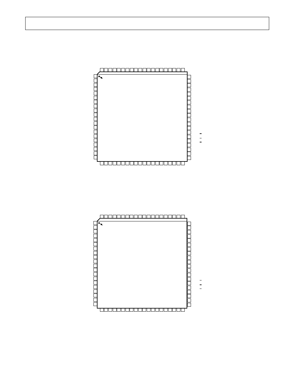
PIN CONFIGURATIONS
Parallel Output Data
80 79 78 77 76
71 70 69 68 67 66 65
75 74 73 72
64 63 62 61
1
2
3
4
5
6
7
8
9
10
11
13
14
15
16
12
17
18
20
19
60
59
58
57
56
55
54
53
52
51
50
49
48
47
46
45
44
43
42
41
21 22 23 24 25 26 27 28 29 30 31 32 33 34 35 36 37 38 39 40
PIN 1
IDENTIFIER
TOP VIEW
(Not to Scale)
D7
(MSB) OUT15
OUT14
VDD
OUT13
OUT12
OUT11
VSS
OUT10
OUT9
OUT8
OUT7
VDD
OUT6
OUT5
OUT4
D6
D5
D4
VSS
D3
D2
D1
VDD
D0
DS
DTACK
R/W
VSS
MODE
A2
A1
OUT0 (LSB)
A/B
OUT
I/Q
OUT
VDD
DV
OUT
PAR/SER
RESET
TRST
TCK
TMS
TDO
TDI
VDD
SYNC NCO
SYNC CIC
SYNC RCF
VSS
EXP2
IN15 (MSB)
IN14
VSS
IN13
IN12
IN11
VDD
IN10
IN9
IN7
VSS
IN6
IN5
IN4
IN8
AD6620
VSS
OUT3
OUT2
OUT1
CLK
A/B
IN0 (LSB)
VDD
IN3
IN2
IN1
A0
CS
EXP0
EXP1
Serial Port
80 79 78 77 76
71 70 69 68 67 66 65
75 74 73 72
64 63 62 61
1
2
3
4
5
6
7
8
9
10
11
13
14
15
16
12
17
18
20
19
60
59
58
57
56
55
54
53
52
51
50
49
48
47
46
45
44
43
42
41
21 22 23 24 25 26 27 28 29 30 31 32 33 34 35 36 37 38 39 40
PIN 1
IDENTIFIER
TOP VIEW
(Not to Scale)
D7
SCLK
SDI
VDD
SDO
SDFS
SDFE
VSS
SBM
WL1
WL0
AD
VDD
NC
NC
NC
D6
D5
D4
VSS
D3
D2
D1
VDD
D0
DS
DTACK
R/W
VSS
MODE
A2
A1
SDIV0
A/B
OUT
I/Q
OUT
VDD
DV
OUT
PAR/SER
RESET
TRST
TCK
TMS
TDO
TDI
VDD
SYNC NCO
SYNC CIC
SYNC RCF
VSS
EXP2
IN15
IN14
VSS
IN13
IN12
IN11
VDD
IN10
IN9
IN7
VSS
IN6
IN5
IN4
IN8
AD6620
VSS
SDIV3
SDIV2
SDIV1
CLK
A/B
IN0
VDD
IN3
IN2
IN1
A0
CS
EXP0
EXP1
THE HIGHEST NUMBERED BIT IS THE MSB FOR ALL PORTS
NC = NO CONNECT
AD6620
14
REV. A
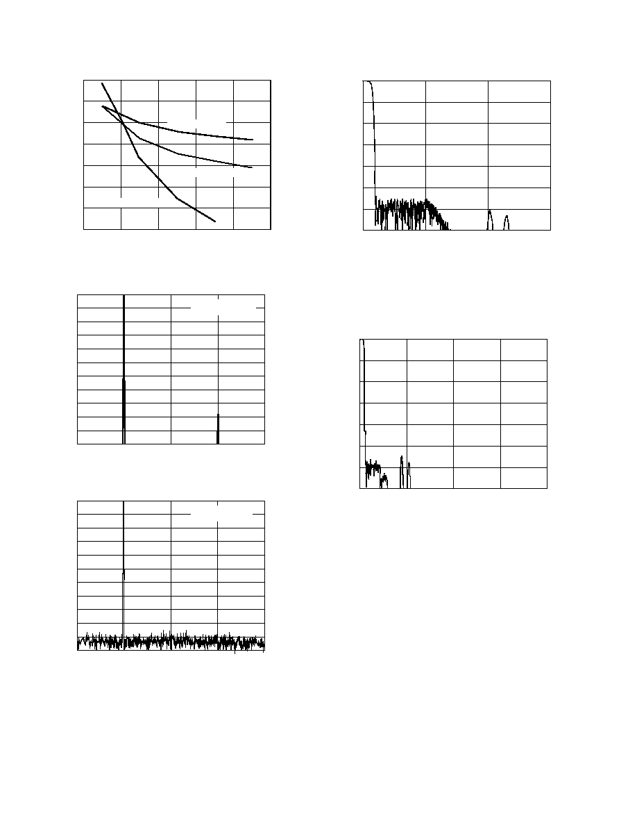
CIC2 DECIMATION
LOG
2
(M)
225
5
1
POWER
mW
2
3
4
250
275
300
325
350
375
400
CIC5 DECIMATION
RCF DECIMATION
TPC 1. Typical Power vs. Decimation Rates
0
132
120
108
96
84
72
60
48
36
24
12
0
f
SAMP
SPUR = 104dB
PHASE DITHER OFF
TPC 2. Typical NCO Spur Without Dither
0
132
120
108
96
84
72
60
48
36
24
12
0
f
SAMP
SPUR = 118dB
PHASE DITHER ON
TPC 3. Typical NCO Spur with Dither
Typical Performance Characteristics
0
1
140
120
100
80
60
40
20
0
REJECTION
dB
COMPOSITE FREQUENCY RESPONSE MHz
2
3
TPC 4. High Decimation GSM Filter
Input sample rate 65 MSPS, decimation is 240, FIR taps is 240.
Unshown spectrum is below that shown. Decimation distribu-
tion is 3, 10, 8, respectively.
0
2
140
120
100
80
60
40
20
0
REJECTION
dB
COMPOSITE FREQUENCY RESPONSE MHz
4
8
6
TPC 5. High Decimation AMPS Filter
Input sample rate 58.32 MSPS, decimation is 300, FIR taps is
128. Unshown spectrum is below that shown. Decimation distri-
bution among CIC2, CIC5, and RCF is 10, 30 and 1, respectively.
AD6620
15
REV. A
INPUT DATA PORT
The input data port accepts a clock (CLK), a 16-bit mantissa
IN[15:0], a 3-bit exponent EXP[2:0], and channel select Pin A/B.
These pins allow direct interfacing to both standard fixed-point
ADCs such as the AD9225 and AD6640, as well as to gain-
ranging ADCs such as the AD6600. These inputs are not 5 V
tolerant and the ADC I/O should be set to 3.3 V.
The input data port accepts data in one of three input modes:
Single Channel Real, Diversity Channel Real, or Single Channel
Complex. The input mode is selected by programming the Input
Mode Control Register located at internal address space 300h.
Single Channel Real mode is used when a single channel ADC
drives the input to the AD6620. Diversity Channel Real mode is
the two channel mode used primarily for diversity receiver appli-
cations. Single Channel Complex mode accepts complex data in
conjunction with the A/B input which identifies in-phase and
quadrature samples (primarily for cascaded 6620s).
The input data port is sampled on the rising edge of CLK at a
maximum rate of 67 MSPS. The 16-bit mantissa, IN[15:0] is
interpreted as a twos complement integer. For most applications
with ADCs having fewer than 16 bits, the active bits should be
MSB justified and the unused LSBs should be tied low.
The 3-bit exponent, EXP[2:0] is interpreted as an unsigned
integer. The exponent can be modified by the 3-bit exponent
offset ExpOff (Control Register 0x305, Bits (75)) and an expo-
nent invert ExpInv (Control Register 0x305, Bit 4).
ExpOff sets the offset of the input exponent, EXP[2:0]. ExpInv
determines the direction of this offset. Equations below show
how the exponent is handled.
scaled input
IN
ExpInv
Exp ExpOff
_
,
mod(
, )
=
×
=
+
2
0
8
scaled input
IN
ExpInv
Exp ExpOff
_
,
mod(
, )
=
×
=
+
2
1
7
8
where: IN is the value of IN[15:0], Exp is the value of EXP[2:0],
and ExpOff is the value of ExpOff.
Input Scaling
In general there are two reasons for scaling digital data. The
first is to avoid "clipping" or, in the case of the AD6620 regis-
ter, "wrap-around" in subsequent stages. Wrap-around is not a
concern for the input data since the NCO is designed to accept
the largest possible input at the AD6620 data port.
The second use of scaling is to preserve maximum dynamic
range through the chip. As data flows from one stage to the next
it is important to keep the math functions performed in the
MSBs. This will keep the desired signal as far above the noise
floor as possible, thus maximizing signal-to-noise ratio.
Scaling with Fixed-Point ADCs
For fixed-point ADCs, the AD6620 exponent inputs EXP[2:0]
are typically not used and should be tied low. The ADC outputs
are tied directly to the AD6620 Inputs, MSB-justified. The
exponent offset (ExpOff) and exponent invert (ExpInv) should
both be programmed to 0. Thus the input equation,
scaled input
IN
ExpInv
Exp ExpOff
_
,
mod(
, )
=
×
=
+
2
0
8
where: IN is the value of IN[15:0], Exp is the value of EXP[0:2],
and ExpOff is the value of ExpOff, simplifies to,
scaled
input
IN
_
mod( , )
=
× 2
0 8
Thus for fixed-point ADCs, the exponents are typically static
and no input scaling is used in the AD6620.
IN4
IN3
IN2
IN1
IN0
EXP2
EXP1
EXP0
IN15
D11 (MSB)
D0 (LSB)
AD6640
AD6620
A/B
+3.3V
Figure 21. Typical Interconnection of the AD6640 Fixed
Point ADC and the AD6620
Scaling with Floating-Point ADCs
An example of the exponent control feature combines the AD6600
and the AD6620. The AD6600 is an 11-bit ADC with three bits
of gain ranging. In effect, the 11-bit ADC provides the mantissa,
and the three bits of relative signal strength indicator (RSSI) are
the exponent. Only five of the eight available steps are used by
the AD6600. See the AD6600 data sheet for additional details.
For gain-ranging ADCs such as the AD6600,
scaled input
IN
ExpInv
Exp ExpOff
_
,
mod(
, )
=
×
=
+
2
1
7
8
where: IN is the value of IN[15:0], Exp is the value of EXP[2:0],
and ExpOff is the value of ExpOff.
The RSSI output of the AD6600 numerically grows with increas-
ing signal strength of the analog input (RSSI = 5 for a large
signal, RSSI = 0 for a small signal). With the Exponent Offset
equal to zero and the Exponent Invert Bit equal to zero, the
AD6620 would consider the smallest signal at the parallel input
(EXP = 0) the largest and, as the signal and EXP word increase,
it shifts the data down internally (EXP = 5, will shift the 11-bit
data right by 5 bits internally before going into the CIC2). The
AD6620 regards the largest signal possible on the AD6600 as
the smallest signal. Thus the Exponent Invert Bit is used to make
the AD6620 exponent agree with the AD6600 RSSI. When it
is set high, it forces the AD6620 to shift the data up for growing
EXP instead of down. The exponent invert bit should always be
set high for use with the AD6600.
Table I. AD6600 Transfer Function with AD6620 ExpInv = 1,
and No ExpOff
ADC Input
AD6600
AD6620
Signal
Level
RSSI[2.0]
Data
Reduction
Largest
101 (5)
4 (>> 2)
12 dB
100 (4)
8 (>> 3)
18 dB
011 (3)
16 (>> 4)
24 dB
010 (2)
32 (>> 5)
30 dB
001 (1)
64 (>> 6)
36 dB
Smallest
000 (0)
128 (>> 7)
42 dB
(ExpInv = 1, ExpOff = 0)
AD6620
16
REV. A
The Exponent Offset is used to shift the data right. For example,
Table I shows that with no ExpOff shift, 12 dB of range is
lost when the ADC input is at the largest level. This is undesired
because it lowers the Dynamic Range and SNR of the system
by reducing the signal of interest relative to the quantization
noise floor.
To avoid this automatic attenuation of the full-scale ADC sig-
nal, the Exponent Offset is used to move the largest signal (RSSI =
5) up to the point where there is no downshift. In other words,
once the Exponent Invert bit has been set, the Exponent Offset
should be adjusted so that mod(75 + ExpOff,8) = 0. This is
the case when Exponent Offset is set to 6 since mod(8, 8) = 0.
Table II illustrates the use of ExpInv and ExpOff when used
with the AD6600 ADC.
Table II. AD6600 Transfer Function with AD6620 ExpInv = 1,
and ExpOff = 6
ADC Input
AD6600
AD6620
Signal
Level
RSSI[2.0]
Data
Reduction
Largest
101 (5)
1 (>> 0)
0 dB
100 (4)
2 (>> 1)
6 dB
011 (3)
4 (>> 2)
12 dB
010 (2)
8 (>> 3)
18 dB
001 (1)
16 (>> 4)
24 dB
Smallest
000 (0)
32 (>> 5)
30 dB
(ExpInv = 1, ExpOff = 6)
This flexibility in handling the exponent allows the AD6620 to
interface with other gain ranging ADCs besides the AD6600.
The Exponent Offset can be adjusted to allow up to seven
RSSI(EXP) ranges to be used as opposed to the AD6600s five.
It also allows the AD6620 to be tailored in a system that employs
the AD6600, but does not utilize all of its signal range. For
example, if only the first four RSSI ranges are expected to occur
then the Exponent Offset could be adjusted to five, which would
then make RSSI = 4 correspond to the 0 dB point of the AD6620.
IN4
IN3
IN2
IN1
IN0
EXP2
EXP1
EXP0
IN15
D10 (MSB)
D0 (LSB)
AD6600
AD6620
A/B
RSS12
RSS11
RSS10
A/B OUT
Figure 22. Typical Interconnection of the AD6600 Gain-
Ranging ADC and the AD6620 in a Diversity Application
Input Timing
The CLK signal is used to sample the input port and clock the
synchronous signal processing stages that follow. The CLK signal
can operate up to 67 MHz and have a duty cycle of 45% to
55%. In applications using high speed ADCs, the ADC sample
clock is typically used to clock the AD6620. Applications that
require a faster signal processing clock than the ADC sample
clock, may employ fractional rate input timing as shown in the
following sections. The input timing requirements vary according
to the mode of operation. Fractional rate input timing creates a
longer "don't care" time for the input data so that slower ADCs
need only meet the setup-and-hold conditions for their data
with respect to their own sample clock cycle, rather than the
faster signal processing clock. The ADC sample clock may be
any integer fraction of CLK up to and including 1, as long as
the clock and data rate are less than or equal to 67 MSPS.
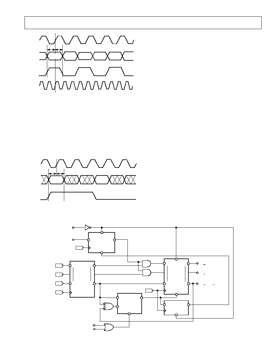
Single Channel Real Mode
In the Single Channel Real mode the A/B input pin functions as
an active high input enable. If the A/D sample clock is fast enough
to perform the necessary filter functions, full rate input timing
can be used and A/B should be tied high as shown in Figure 23.
N
N+1
N+2
N+3
N+4
t
SI
t
HI
CLK
IN[15:0]
EXP[2:0]
A/B
Figure 23. Full Rate Input Timing, Single Channel
Real Mode
When a faster processing clock is used to achieve better filter
performance, the A/D data must be synchronized with the faster
AD6620 CLK signal. This is achieved by having the ADC clock
rate an integer fraction of the AD6620 clock rate. AD6620 input
data is sampled at the slower ADC clock rate. In the Single
Channel Real Mode this is achieved by dynamically controlling
the A/B input and bringing it high before each rising CLK edge
that data is to be sampled on. A/B must be returned low before
the next high speed clock pulse and the duty cycle of the A/B
signal will therefore be equal to the data-to-clock ratio.
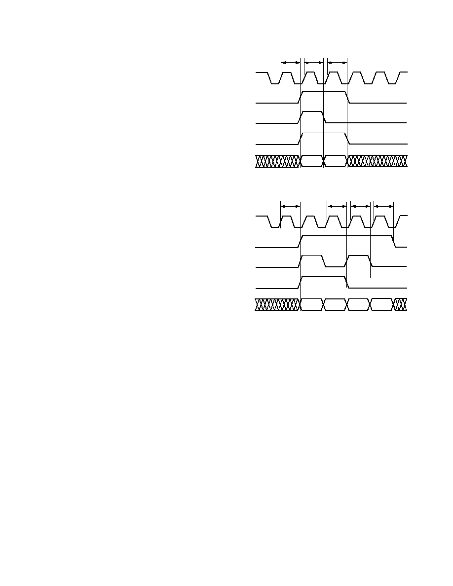
N
N+1
t
SI
t
HI
CLK
IN[15:0]
EXP[2:0]
A/B
Figure 24. Fractional Rate Input Timing (4
× CLK), Single
Channel Real Mode
Diversity Channel Real Mode
In the Diversity Channel Real mode the A/B pin serves not only
as an input enable but also to determine which channel is being
sampled on a given CLK edge. A high on the A/B pin marks
channel A data and a low on A/B marks channel B data. The
AD6620 only accepts the first sample after an A/B transition.
All subsequent samples are disregarded until A/B changes again.
When full rate input timing is employed in the Diversity Chan-
nel Real mode, A/B must toggle on every rising edge of CLK for
new data to be clocked into the AD6620.
AD6620
17
REV. A
t
SI
t
HI
CLK
IN[15:0]
EXP[2:0]
A/B
B
N
B
N+1
A
N+1
A
N+2
B
N+2
CLK
2x
A
N
IF CLK 2x IS USED TO CLOCK THE AD6620, THE FIRST RISING EDGE AFTER
THE A/B TRANSITION WILL LATCH THE DATA.
Figure 25. Full Rate Input Timing, Diversity Channel Real
Mode
If fractional rate input timing is necessary in the Diversity Chan-
nel Real Mode, the A/B pin must toggle at half the rate of the
A/D sample clock. The timing diagram below shows a 3
× pro-
cessing clock. In this situation there will be one ADC encode
pulse for every three AD6620 CLK pulses and data must be
taken on every third CLK pulse. The CLK edges that corre-
spond to the latching of A and B channel data are shown in
Figure 26.
A
N
t
SI
t
HI
CLK
IN[15:0]
EXP[2:0]
A/B
B
N
Figure 26. Fractional Rate Input Timing (3
× CLK), Diversity
Channel Real Mode
Single Channel Complex Mode
In the Single Channel Complex input mode, A/B high identi-
fies the in-phase samples and A/B low identifies quadrature
samples. The quadrature samples are paired with the previous
in-phase samples. The timing for this mode is the same as that
of the Diversity Channel Real Mode. This mode is useful for
accepting complex output data from another AD6620 or another
source to increase filtering and or decimation rates.
In the Single Channel Complex Mode the CIC2 decimation
must be set to two (M
CIC2
= 2). This is necessary in order to
allow enough CLK cycles to process the complex input data as
described below.
First clock cycle: (A/B high).
I data loaded from the input port.
The I data-path gets I
× cosine.
The Q data-path gets I
× sine.
The first integrator of the CIC2 adds these values to its
previous sums.
The rest of the CIC2 is idle.
Second clock cycle: (A/B low).
Q data loaded from the input port.
The I data-path gets Q
× sine.
The Q data-path gets Q
× cosine.
The first integrator of the I path of the CIC2 completes the
sum (I
× cosine - Q × sine) and the first integrator of the Q
path of the CIC2 completes the sum j(I
× sine + Q × cosine).
The rest of the CIC2 operates on these sums, which is the
complete complex multiply. The data is then multiplexed
through the rest of the chip as if it were single channel real data.
Simplified Input Data Port Schematic
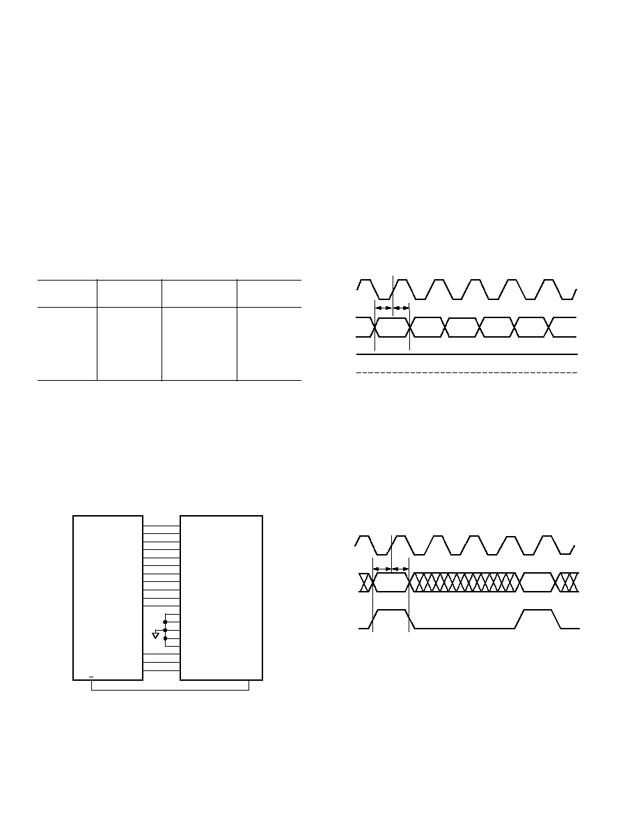
Figure 27 details a simplified schematic for the input data port.
The first thing to note is that IN[15:0], EXP[2:0] and A/B are
all synchronously latched with CLK. Note also that upon soft
reset, a seven pipeline delay (sample clock delay) exists in the
data path. This delay is synchronous with CLK, but is in fact
seven valid sample data delays. For instance, in single channel
CLK
LOGIC "1"
SOFT RESET
CLR
Q
Q
D
ENB
Q
D
IN[15:0]
EXP[2:0]
Q
D
A/B
CLK
REGISTER
Q
D
Q
D
REGISTER
CLK
MULTIPLEXER
D
S
1
S
2
C
DUAL CHANNEL REAL
SINGLE CHANNEL COMPLEX
INT IN[15:0]
INT EXP[2:0]
INT DATA STROBE
CLR
DELAY 7
ENB
D
SET
Q
CLR
Q
Figure 27. Simplified Input Data Port Schematic for the AD6620
AD6620
18
REV. A
real mode with full rate timing the delay is seven CLKs. If
instead the data rate is one-fourth CLK, then 28 CLKs (i.e.,
seven sample data delays, gated via A/B) occur before valid data
is passed to the NCO stage.
Interfacing AD6620 Inputs to 5 V Logic Gates
None of the inputs to the AD6620 are tolerant of 5 V logic
signals. When interfacing 5 V devices to this product, an interface
gate such as the 74LCX2244 is recommended. If latching must
be performed, 74LCX574 latches may be used. This gate runs
from the 3.3 V supply and is tolerant of 5 V inputs.
OUTPUT DATA PORT
Parallel Output Data Port
The AD6620 provides a choice of two output ports: a 16-bit
parallel port and a synchronous serial port. Output operation
using the serial port is discussed in the next section. The parallel
port is limited to 16 bits. Because pins are shared between the
parallel and serial output ports, only one output mode can be
used. The output mode must be set with a hard reset generated
by at least a 30 ns low time on the
RESET pin. If the PAR/SER
line is high (Logic "1"), then parallel output data is activated.
The PAR/SER pin should remain static after the output mode
has been set (i.e., PAR/SER should only change when
RESET is
low). Data out of the AD6620 is two's complement.
A scale factor is associated with the output port, which allows
the signal level to be adjusted. This scale factor is mapped to
location 309h, Bits 20 in the AD6620 internal address space.
This scalar controls the weight of the 16-bit data going to the
parallel port. The scale factor is discussed in the RAM Coeffi-
cient Filter (RCF) section.
The Parallel Mode provides a 16-bit output port, which consti-
tutes the I and Q data for either one or both channels. This port
can run at a maximum of 67 MHz (33.5 MHz I, 33.5 MHz Q).
This rate assumes that there is a minimum decimation of 2 in
the first filter stage (CIC2) or a 2
× or greater CLK is used. This
decimation is required because for every input word there is
both an I and a Q output. When the data rate and clock rate are
the same (Full Rate Input Timing), the minimum decimation of
2 must occur in CIC2. Refer to CIC2 for more detail.
DV
OUT
DV
OUT
is provided to signal that valid data is present. If this pin
is high, there is a valid data word on the bus. DV
OUT
remains high
for two high-speed clock cycles in Single Channel Real and Single
Channel Complex Mode and for four high-speed clock cycles in
Diversity Channel Real mode. After DV
OUT
returns low the Q data
will remain until the next data sample.
I/Q
OUT
When this pin is high the data word represents I data; when
I/Q
OUT
is low Q data is present. This signal will also be low when
DV
OUT
is low since the last word of every data phase is Q data.
A/B
OUT
If DV
OUT
is low, A/B
OUT
is always low. When A/B
OUT
is high, A
Channel data is available on the output. If DV
OUT
remains high
while A/B
OUT
is low, then B Channel data is on the output pins
of the chip OUT[15:0].
CLK
OUT[15:0]
VALID DATA
A DATA
t
DPR
t
DPF
t
DPF
I
Q
I
A
Q
A
DV
OUT
I/Q
OUT
A/B
OUT
Figure 28. Parallel Output Data Timing (Single-Channel
Mode)
t
DPR
t
DPF
t
DPF
t
DPF
I
Q
I
Q
I
A
Q
A
I
B
Q
B
VALID DATA
A DATA
B DATA
CLK
OUT[15:0]
DV
OUT
I/Q
OUT
A/B
OUT
Figure 29. Parallel Output Data Timing (Diversity Channel
Mode)
Serial Output Data Port
The AD6620 provides a choice of two output ports: a 16-bit
parallel port and a synchronous serial port. The advantage of
using the serial port is that all 23 bits of available data can be
output in the 24-bit or 32-bit mode. The serial output port
shares some of the same pins used by the parallel output port.
As a result, one or the other mode of output may be utilized,
but not both. The output mode must be set with a hard reset
generated by at least a 30 ns low time on the
RESET pin. If the
PAR/SER line is low (Logic "0") upon reset, then serial output
data is activated. The PAR/SER pin should remain static after
the output mode has been set (i.e., PAR/SER should only change
when
RESET is low).
Note that the AD6620 cannot be booted through the serial port.
The microport must be used to initialize the device, then serial
operation is supported.
Figure 30 shows the typical interconnections between an AD6620
in serial master mode and a DSP. Refer to the Serial Control
Port section for a detailed description of pin functions and pro-
cedures for writing and reading with relation to the serial port.
Note the 10 k
resistors connected to SDI and SDO. These
prevent the lines from toggling when the AD6620 or DSP
three-states these pins.
AD6620
19
REV. A
SCLK
AD6620
DSP
+3.3V
SBM
SCLK
SDI
DT
SDO
DR
SDFS
RFS
SDFE
10k
10k
SDIV
2
4
AD
WL
Figure 30. Typical Serial Data Output Interface to DSP
(Serial Master Mode, SBM = 1)
Figure 31 shows two AD6620s illustrating the cascade capability
for the chip. The first is connected as a serial master and the
second is configured in serial cascade mode. The SDFE signal
of the master is connected to the SDFS of the slave. This allows
the master AD6620 data to be obtained first by the DSP, fol-
lowed by the cascaded AD6620 data.
SCLK
AD6620
DSP
+3.3V
SBM
SCLK
SDI
DT
SDO
DR
SDFS
RFS
SDFE
10k
SDIV
2
4
AD
WL
10k
SCLK
AD6620
CASCADE
SBM
SDI
SDO
SDFS
SDFE
SDIV
2
4
AD
WL
Figure 31. Typical Serial Data Output Interface to DSP
(Serial Cascade Mode, SBM = 0)
The AD6620 also supports a serial slave mode, where the serial
clock and interface is provided by a DSP or ASIC that is set to
operate in the master mode. Note that the AD6620 cannot be
booted through the serial port. The microport must be used to
initialize the device, then serial operation is supported.
In the serial slave mode, DV
OUT
is valid and indicates the pres-
ence of a new word in the output buffers of the shift register.
This pin may thus be used by the DSP to generate an interrupt
to service the serial port. The DSP then generates an SFDS
pulse to drive the AD6620. The first serial clock rising edge
after SDFS makes the first bit available at SDO. The falling
edge of serial clock can be used to sample the data. The total
number of bits are then read from the AD6620 (determined by
the serial port word length). If the DSP has the ability to count
bits, the DSP will know when the complete frame is read. If not,
the DSP can monitor the SDFE pin to determine that the com-
plete frame is read. The serial clock provided by the DSP can be
asynchronous with the AD6620 clock and input data.
SCLK
AD6620
DSP
SBM
SCLK
SDI
DT
SDO
DR
SDFS
RFS
SDFE
10k
10k
SDIV
2
4
AD
WL
DV
OUT
IRQ
Figure 32. Typical Serial Data Output Interface to DSP
(Serial Slave Mode, SBM = 0)
In either the serial master or slave mode, there are two con-
straints that must be observed. The first is that the clock must
be fast enough to read the serial frame prior to the next frame
becoming available. Since the AD6620 output is synchronous
with its input sample rate, the output update rate can be deter-
mined by the user-programmed decimation rate. The timing
diagram in Figure 33 details how serial slave mode is imple-
mented. The second constraint is that the time between serial
frames may be either zero SCLK periods (the end of one frame
adjoins the beginning of the next) or two or more SCLK peri-
ods. One SCLK period between frames is not allowed.
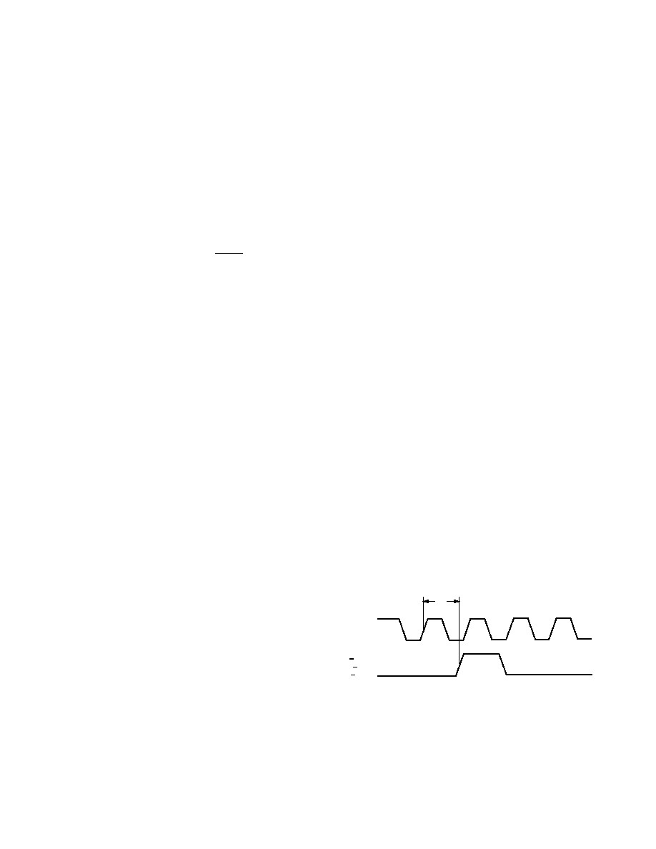
t
DSO
DV
OUT
SCLK
SDFS
SDO
DSP USES FALLING EDGE OF
DV
OUT
TO GENERATE SDFS
FIRST DATA IS AVAILABLE THE FIRST
RISING SCLK AFTER SDFS GOES HIGH
I
MSB
I
MSB 1
DV
OUT
PULSEWIDTH IS 2 CLKIN
SINGLE CHANNEL AND 4 CLKIN
DUAL CHANNEL
Figure 33. Timing for Serial Slave Mode (SBM = 0)
FREQUENCY TRANSLATOR
The first signal processing stage is a frequency translator con-
sisting of two multipliers and a 32-bit complex numerically
controlled oscillator (NCO). The NCO serves as a quadrature
local oscillator capable of producing any analytic frequency
between f
SAMP
/2 and +f
SAMP
/2 with a resolution of f
SAMP
/2
32
. In
the Single Channel Real input mode, f
SAMP
is equal to f
CLK
multi-
plied by the fraction of CLK cycles that A/B is high. In the
Diversity Channel Real and Single Channel Complex input
AD6620
20
REV. A
modes, f
SAMP
is equal to f
CLK
multiplied by the fraction of CLK
cycles on which A/B has been toggled. The NCO worst case
discrete spur is better than 100 dBc for all output frequencies.
The control word, NCO_FREQ is interpreted as a 32-bit unsigned
integer. To translate a channel centered at f
CH
to dc, calculate
NCO_FREQ using the equation below. The mod function is
used here to allow for Super Nyquist sampling where the IF
carrier (fCH) is larger than the sample rate (fSAMP). The mod
removes the integer portion of the number and forces it into the
32-bit NCO Frequency Register. If the fraction remaining is
larger than 0.5, the NCO will be tuning above the Nyquist rate.
The corresponding signal is then aliased back into the first Nyquist
Zone as a negative frequency.
NCO
FREQ
f
f
CH
SAMP
_
,
=
×
2
1
32
mod
In both Single and Diversity Channel Real Input modes, the out-
put of the translation stage is the complex product of the real
input samples and the complex samples from the NCO. It is
necessary for the subsequent decimating filters to reject the
unwanted image of the channel of interest, as well as any unwanted
neighboring signals (and their images) not rejected by previ-
ous analog filters.
In the Diversity Channel Real Input mode, the same NCO output
words are used for both channel A and B streams, resulting in
identical phase shifts. In Single Channel Complex mode both I
and Q inputs are multiplied by the quadrature outputs of the
NCO. The I and Q products of the multiply are then processed
in the AD6620 filter stages.
In single channel real or dual channel real operation, the frequency
translation and filtering processes provide a gain of 6 dB. This
can be visualized since the input data is usually a real sampled
signal consisting of both positive and negative frequency compo-
nents (Figure 2a). After being mixed with the complex NCO,
the normal filtering of the AD6620 will remove one component
or the other resulting in an analytic signal (Figure 2b). This
filtering thus removes one-half or 6 dB of the signal keeping
consistent with the mathematics involved. If however, the filter-
ing of the device allows both the positive and negative frequency
components to pass (i.e., the original signal is near dc), the gain
of the frequency translation is 0 dB. Finally, if the NCO is
bypassed, the gain of the frequency translation block is 12 dB.
Phase Dither
The AD6620 provides a phase dither option for improving the
spurious performance of the NCO. This is controlled via the
NCO Control Register at address 301 hex. When phase dither is
enabled by setting Bit 1 of this register high, spurs due to phase
truncation in the NCO are randomized. The energy from these
spurs is spread into the noise floor and Spurious Free Dynamic
Range is increased at the expense of very slight decreases in the
SNR. Phase dither should be experimented with for each desired
NCO frequency and if it is seen to reduce spurs, it should be
considered. The choice of whether Phase Dither is used in a
system will ultimately be decided by the system goals. If lower
spurs are desired at the expense of a slightly raised noise floor, it
should be employed. If a low noise floor is desired and the higher
spurs can be tolerated or filtered by subsequent stages, then
Phase Dither is not needed.
Amplitude Dither
The second dither option is Amplitude Dither or "Complex
Dither." Amplitude Dither is enabled by setting Bit 2 of the
NCO Control Register at address 0x301 high. Amplitude Dither
improves performance by randomizing the amplitude quantiza-
tion errors within the angular to Cartesian conversion of the
NCO. This dither will be particularly useful when the NCO
frequency is close to an integer submultiple of the Input Data
Rate. However, this option may reduce spurs at the expense of a
slightly raised noise floor. Amplitude Dither and Phase Dither
can be used together, separately or not at all.
Phase Offset
The phase offset register adds an offset to the phase accumula-
tor of the NCO. This is a 16-bit register and is interpreted as a
16-bit unsigned integer. A 0 in this register corresponds to a 0
Radian offset and an FFFF hex corresponds to an offset of 2
(1 1/(2^16)) Radians. This register can be used to allow mul-
tiple AD6620s whose NCOs are synchronized to produce sine
waves with a known and steady phase difference.
NCO Synchronization
In order to achieve phase coherence between several AD6620s,
a SYNC_NCO pin is provided. When the internal register
bit, SYNC_M/S (Bit 3 of internal register 0x300), is set high,
SYNC_NCO provides a synchronization pulse on the rising
edge of CLK. When the SYNC_M/S bit is low, SYNC_NCO
accepts an external synchronization signal sampled on the rising
edge of CLK. When the AD6620 is a slave, the SYNC_NCO
signal need not be a short pulse. It may be taken high and held
for more than a CLK cycle in which case the NCO will be held
inactive until this pin is again lowered. If the device is run as a
sync slave in Single Channel Mode, the SYNC_NCO pin must
be held low for one sample period, usually one clock cycle. If the
device is run in Diversity Channel Real mode, the SYNC_NCO
must be high for two sample periods (clock cycles). In a system
with an array of AD6620s it is not necessary to use one as a
master. It may be desirable to generate a synchronization signal
elsewhere in the system and use that to control the AD6620. An
example of this may be in systems that receive packets of data.
In this case, the NCO may be resynchronized prior to the begin-
ning of the packet, thus giving a consistent phase relationship on
each burst. This allows for ease of use in a large system where
many AD6620s need be synchronized accurately across a large
backplane or installation.
t
DY
CLK
SYNC NCO
SYNC CIC
SYNC RCF
NOTE:
IN THE SLAVE MODE WITH SINGLE CHANNEL OPERATION, THE WIDTH
OF THE SYNC_NCO SHOULD BE ONE SAMPLE CLOCK CYCLE. IN DUAL
CHANNEL MODE, THE PULSEWIDTH SHOULD BE TWO SAMPLE CLOCK
CYCLES. IF A PULSE LONGER THAN SPECIFIED IS USED, THE NCO WILL
BE INHIBITED AND NOT INCREMENT PROPERLY.
Figure 34. SYNC_NCO Pin
AD6620
21
REV. A
The frequency of the SYNC_NCO pulses, and therefore the
accuracy of the synchronization, is determined by the value of
the NCO Sync Control Register at address 302 hex. The value
in this register is the SYNC_MASK and is interpreted as a
32-bit unsigned integer. This value controls the window around
the zero crossing of the NCO output sine wave in which the
NCO will output a SYNC_NCO pulse as a master. As a slave,
the value in this register will determine the number of MSBs
of the output sine wave that are synchronized with the master.
The Master and all slaves should use the same SYNC_MASK
word. This value should almost always be written as all 1s
(FFFFFFFF hex).
Effects of A/B Input on the NCO
If the AD6620 is run in Single Channel Real mode using frac-
tional rate input timing, the A/B input is used to enable the
NCO advancement. If the A/B line is held high longer than one
clock period, the NCO will advance for each rising edge of the
CLK while A/B is high. This is not normally the desired result
and thus A/B must be taken low after the first CLK period to
prevent anomalous NCO results. See additional details under
Fractional Rate Timing.
Phase Continuous Tuning with the AD6620
For synchronization purposes, the AD6620 NCO phase is reset
each time the NCO frequency register is either written to or
read from. This is accomplished by forcing an NCO Sync to
occur. Normally, phase-continuous tuning is required on the
transmit path to control spectral leakage. On the receive path
this in not usually a constraint. However, if phase-continuous
tuning is required with the AD6620, it can be accomplished by
configuring the AD6620 as a Sync Slave. In this manner, no
internal NCO sync is generated when the NCO frequency regis-
ter is written to. If multiple AD6620s are synchronized together,
a common external sync pulse can be used to lock each of the
receivers together at the appropriate point in time. It is also
possible to reconfigure the AD6620 after the NCO frequency
register has been written so that the chip is once again a Sync
Master. The next time the NCO phase cycles through 0 degrees,
the NCO sync is exerted and the chip is again synchronized.
2ND ORDER CASCADED INTEGRATOR COMB FILTER
The CIC2 filter is a fixed-coefficient, decimating filter. It is
constructed as a second order CIC filter whose characteristics
are defined only by the decimation rate chosen. This filter can
process signals at the full rate of the input port (67 MHz) in all
input modes. The output rate of this stage is given by the equa-
tion below.
f
f
M
SAMP
SAMP
CIC
2
2
=
The decimation ratio, MCIC2, is an unsigned integer that may
be between 1 and 16. This stage may be bypassed under certain
conditions by setting, M
CIC2
equal to 1. For this to happen the
processing clock rate, f
CLK
must be two or more times the input
data rate, f
SAMP
. This is because the I and Q data is processed in
parallel within the CIC2 filter, and the I and Q output data is
then multiplexed through the same data pipe before it enters the
CIC5 filter.
The frequency response of the CIC2 filter is given by the follow-
ing equations.
H z
z
z
S
M
CIC
CIC
( )
=
×
1
2
1
1
2
2
1
2
H f
M
f
f
f
f
S
CIC
SAMP
SAMP
CIC
( )
sin
sin
=
×
×
1
2
2
2
2
The scale factor, S
CIC2
is a programmable unsigned integer
between 0 and 6. This serves as an attenuator that can reduce
the gain of the CIC2 in 6 dB increments. For the best dynamic
range, S
CIC2
should be set to the smallest value possible (i.e.,
lowest attenuation) without creating an overflow condition.
This can be safely accomplished using the equation below, where
input_level is the largest fraction of full scale possible at the
input to this AD6620 (normally 1). The CIC2 scale factor is
not ignored when the CIC2 is bypassed.
REGISTER
REGISTER
1
MASKED
COUNT = 0?
SYNC
MASK
SYNC_NCO
PIN
1
1
32
32
32
32
1
0
32
32
32
32
32
NCO FREQ
AMPLITUDE
DITHER
COS
SIN
PHASE
DITHER
PHASE
OFFSET
PHASE
ACCUMULATOR
X4
REGISTER
Figure 35. NCO Block Diagram
AD6620
22
REV. A
S
ceil
M
input
level
OL
input
level
CIC
CIC
CIC
S
CIC
2
2
2
2
2
1
2
2
=
×
=
×
log (
_
)
_
The equations for calculating CIC2 output level is correct when
stage is not bypassed (normal operation). However, when by-
passed, the following equations should be used instead.
OL
CIC2
= Input Level
The gain and pass band droop of the CIC2 should be calculated
by the equations above, as well as the filter transfer equations
that follow. If these are unacceptable, they can be compensated
for in subsequent stages.
CIC2 Rejection
The table below illustrates the amount of bandwidth in percent
of the data rate into the CIC2 stage. The data in this table may
be scaled to any allowable sample rate up to 67 MHz in Single
Channel Mode or 33.5 MHz in Diversity Channel Mode. The
table can be used as a tool to decide how to distribute the deci-
mation between CIC2, CIC5 and the RCF.
The data in this table may be scaled to any allowable sample
rate up to 67 MHz in Single Channel Mode or 33.5 MHz in
Diversity Channel Mode.
Table III. SSB CIC2 Alias Rejection Table (f
SAMP
= 1)
Bandwidth Shown in Percentage of f
SAMP
M
CIC2
50 dB 60 dB
70 dB
80 dB 90 dB
100 dB
2
1.79
1.007
0.566
0.318
0.179
0.101
3
1.508
0.858
0.486
0.274
0.155
0.087
4
1.217
0.696
0.395
0.223
0.126
0.071
5
1.006
0.577
0.328
0.186
0.105
0.059
6
0.853
0.49
0.279
0.158
0.089
0.05
7
0.739
0.425
0.242
0.137
0.077
0.044
8
0.651
0.374
0.213
0.121
0.068
0.038
9
0.581
0.334
0.19
0.108
0.061
0.034
10
0.525
0.302
0.172
0.097
0.055
0.031
11
0.478
0.275
0.157
0.089
0.05
0.028
12
0.439
0.253
0.144
0.082
0.046
0.026
13
0.406
0.234
0.133
0.075
0.043
0.024
14
0.378
0.217
0.124
0.07
0.04
0.022
15
0.353
0.203
0.116
0.066
0.037
0.021
16
0.331
0.19
0.109
0.061
0.035
0.02
Example Calculations
Goal: Implement a filter with an Input Sample Rate of 10 MHz
requiring 100 dB of Alias Rejection for a
±7 kHz pass band.
Solution: First determine the percentage of the sample rate that
is represented by the pass band.
BW
kHz
MHz
FRACTION
=
×
=
100
7
10
0 07
.
%
Find the 100 dB column on the right of the table and look
down this column for a value greater than or equal to your
pass band percentage of the clock rate. Then look across to the
extreme left column and find the corresponding decimation
rate. Referring to the table, notice that for a decimation of 4, the
frequency having 100 dB of alias rejection is 0.071 percent
which is slightly greater than the 0.07 percent calculated. There-
fore, the maximum bound on CIC2 decimation for this condi-
tion is four. Additional decimation means less alias rejection
than the 100 dB required.
Note that although an M
CIC2
less then four would still yield the
required rejection, overall power consumption is reduced by
decimating as much as possible in this stage. Decimation in
CIC2 lowers the data rate and thus reduces power consumed in
subsequent stages.
The plot below shows the CIC2 transfer function using a deci-
mation of four. The first plot is referenced to the input sample
rate, the complex spectrum from f
SAMP
/2 to f
SAMP
/2. The sec-
ond plot is referenced to the CIC2 output rate, the complex
spectrum from f
SAMP2
/2 to f
SAMP2
/2. The aliases of the CIC2
can be seen to be "folding back" in toward the edge of the
desired filter pass band. It is the level of these aliases as they
move into the desired pass band that are important.
0.5
120
100
80
60
40
20
0
dBFS
f/f
SAMP
0.4 0.3
0.2
0.1
0.1
0.2
0.3
0.4
0.5
0
0.5
120
100
80
60
40
20
0
dBFS
f/f
SAMP2
0.4 0.3
0.2
0.1
0.1
0.2
0.3
0.4
0.5
0
Figure 36. CIC2 Alias Rejection, M
CIC2
= 4
The set of plots below show a decimation of 16 in the CIC2
filter. The lobes of the filter drop as the decimation rate
increases, but the amplitudes of the aliased frequencies increase
because the output rate has been reduced.
AD6620
23
REV. A
The frequency response of the filter is given by the following
equations. The gain and pass band droop of CIC5 should be
calculated by these equations. Both parameters may be compen-
sated for in the RCF stage.
H z
z
z
S
M
CIC
CIC
( )
=
×
+
1
2
1
1
5
5
5
1
5
H f
M
f
f
f
f
S
CIC
SAMP
SAMP
CIC
( )
sin
sin
=
×
×
+
1
2
5
5
5
2
2
5
The scale factor, S
CIC5
is a programmable unsigned integer
between 0 and 20. It serves to control the attenuation of the
data into the CIC5 stage in 6 dB increments. For the best dynamic
range, S
CIC5
should be set to the smallest value possible (lowest
attenuation) without creating an overflow condition. This can
be safely accomplished using the equation below, where OL
CIC2
is the largest fraction of full scale possible at the input to this
filter stage. This value is output from the CIC2 stage then pipe-
lined into the CIC5. S
CIC5
is ignored when this filter is bypassed
by setting M
CIC5
= 1.
S
ceil
M
OL
OL
M
OL
CIC
CIC
CIC
CIC
CIC
S
CIC
CIC
5
2
5
5
2
5
5
5
5
2
5
2
5
=
×
(
)
=
(
)
×
+
log (
)
when CIC5 is bypassed;
OL
OL
CIC
CIC
5
2
=
The output rate of this stage is given by the equation below.
f
f
M
SAMP
SAMP
CIC
5
2
5
0.5
120
100
80
60
40
20
0
dBFS
f/f
SAMP
0.4 0.3
0.2
0.1
0.1
0.2
0.3
0.4
0.5
0
0.5
120
100
80
60
40
20
0
dBFS
f/f
SAMP2
0.4 0.3
0.2
0.1
0.1
0.2
0.3
0.4
0.5
0
Figure 37. CIC2 Alias Rejection, M
CIC2
= 16
5TH ORDER CASCADED INTEGRATOR COMB FILTER
The third signal processing stage, CIC5, implements a sharper
fixed-coefficient, decimating filter than CIC2. The input rate to
this filter is f
SAMP2
. The maximum input rate is given by the
equation below. N
CH
equals two for Diversity Channel Real
input mode; otherwise N
CH
equals one. In order to satisfy this
equation, M
CIC2
can be increased, N
CH
can be reduced, or f
CLK
can be increased (reference fractional rate input timing described
in the Input Timing section).
f
f
N
SAMP
CLK
CH
2
2
×
The decimation ratio, M
CIC5
, may be programmed from 1 to 32
(all integer values). When M
CIC5
= 1, this stage is bypassed and
the CIC5 scale factor is ignored.
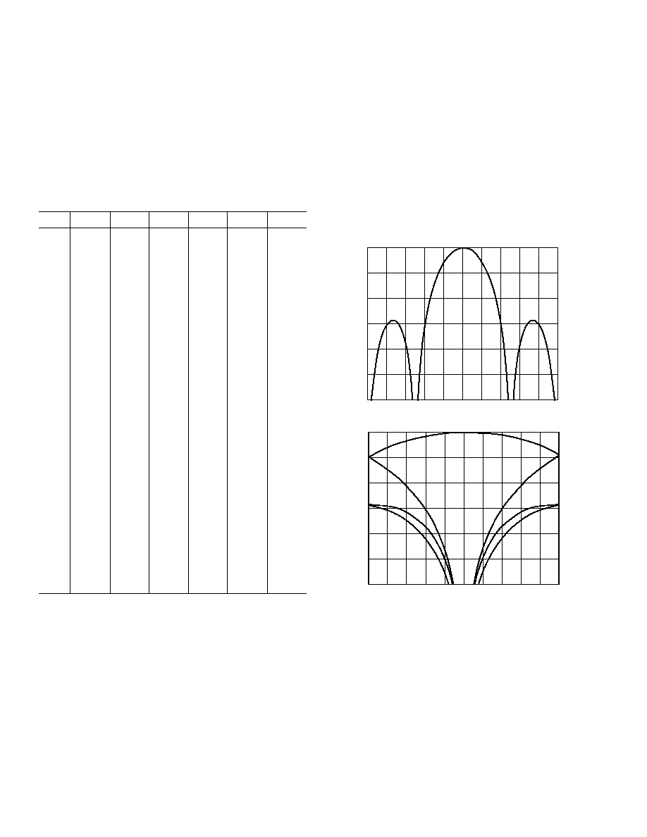
AD6620
24
REV. A
This table helps to calculate an upper bound on decimation,
M
CIC5
, given the desired filter characteristics.
The plots following (Figure 38) represent the CIC5 transfer
function with respect to the CIC5 output rate for a decimation
of 4. The first plot is referenced to the input sample rate and
shows the complex spectrum from f
SAMP/
2 to +f
SAMP
/2. The
second plot is referenced to the CIC5 output rate; the complex
spectrum ranges from f
SAMP5
/2 to +f
SAMP5
/2. Aliased images in
CIC5 "fold back" toward the edge of the desired filter pass
band. It is the level of these aliases as they move into the desired
pass band that are of concern. The improved roll-off of CIC5
over CIC2 can be seen when these plots are compared to those
previously shown for CIC2.
0.5
120
100
80
60
40
20
0
dBFS
f/f
SAMP
0.4 0.3
0.2
0.1
0.1
0.2
0.3
0.4
0.5
0
0.5
120
100
80
60
40
20
0
dBFS
f/f
SAMP5
0.4 0.3
0.2
0.1
0.1
0.2
0.3
0.4
0.5
0
Figure 38. CIC5 Alias Rejection, M
CIC5
= 4
CIC5 Rejection
The table below illustrates the amount of bandwidth in percent-
age of the clock rate that can be protected with various decimation
rates and alias rejection specifications. The maximum input rate
into the CIC5 is 32.5 MHz. As in the previous table, these
are the 1/2 bandwidth characteristics of the CIC5. Note that
the CIC5 stage can protect a much wider band than the CIC2 for
any given rejection.
Table IV. SSB CIC5 Alias Rejection Table (f
SAMP2
= 1)
Bandwidth Shown in Percentage of f
SAMP2
M
CIC5
50 dB 60 dB
70 dB
80 dB 90 dB
100 dB
2
10.227
8.078
6.393
5.066
4.008
3.183
3
7.924
6.367
5.11
4.107
3.297
2.642
4
6.213
5.022
4.057
3.271
2.636
2.121
5
5.068
4.107
3.326
2.687
2.17
1.748
6
4.267
3.463
2.808
2.27
1.836
1.48
7
3.68
2.989
2.425
1.962
1.588
1.281
8
3.233
2.627
2.133
1.726
1.397
1.128
9
2.881
2.342
1.902
1.54
1.247
1.007
10
2.598
2.113
1.716
1.39
1.125
0.909
11
2.365
1.924
1.563
1.266
1.025
0.828
12
2.17
1.765
1.435
1.162
0.941
0.76
13
2.005
1.631
1.326
1.074
0.87
0.703
14
1.863
1.516
1.232
0.998
0.809
0.653
15
1.74
1.416
1.151
0.932
0.755
0.61
16
1.632
1.328
1.079
0.874
0.708
0.572
17
1.536
1.25
1.016
0.823
0.667
0.539
18
1.451
1.181
0.96
0.778
0.63
0.509
19
1.375
1.119
0.91
0.737
0.597
0.483
20
1.307
1.064
0.865
0.701
0.568
0.459
21
1.245
1.013
0.824
0.667
0.541
0.437
22
1.188
0.967
0.786
0.637
0.516
0.417
23
1.137
0.925
0.752
0.61
0.494
0.399
24
1.09
0.887
0.721
0.584
0.474
0.383
25
1.046
0.852
0.692
0.561
0.455
0.367
26
1.006
0.819
0.666
0.54
0.437
0.353
27
0.969
0.789
0.641
0.52
0.421
0.34
28
0.934
0.761
0.618
0.501
0.406
0.328
29
0.902
0.734
0.597
0.484
0.392
0.317
30
0.872
0.71
0.577
0.468
0.379
0.306
31
0.844
0.687
0.559
0.453
0.367
0.297
32
0.818
0.666
0.541
0.439
0.355
0.287
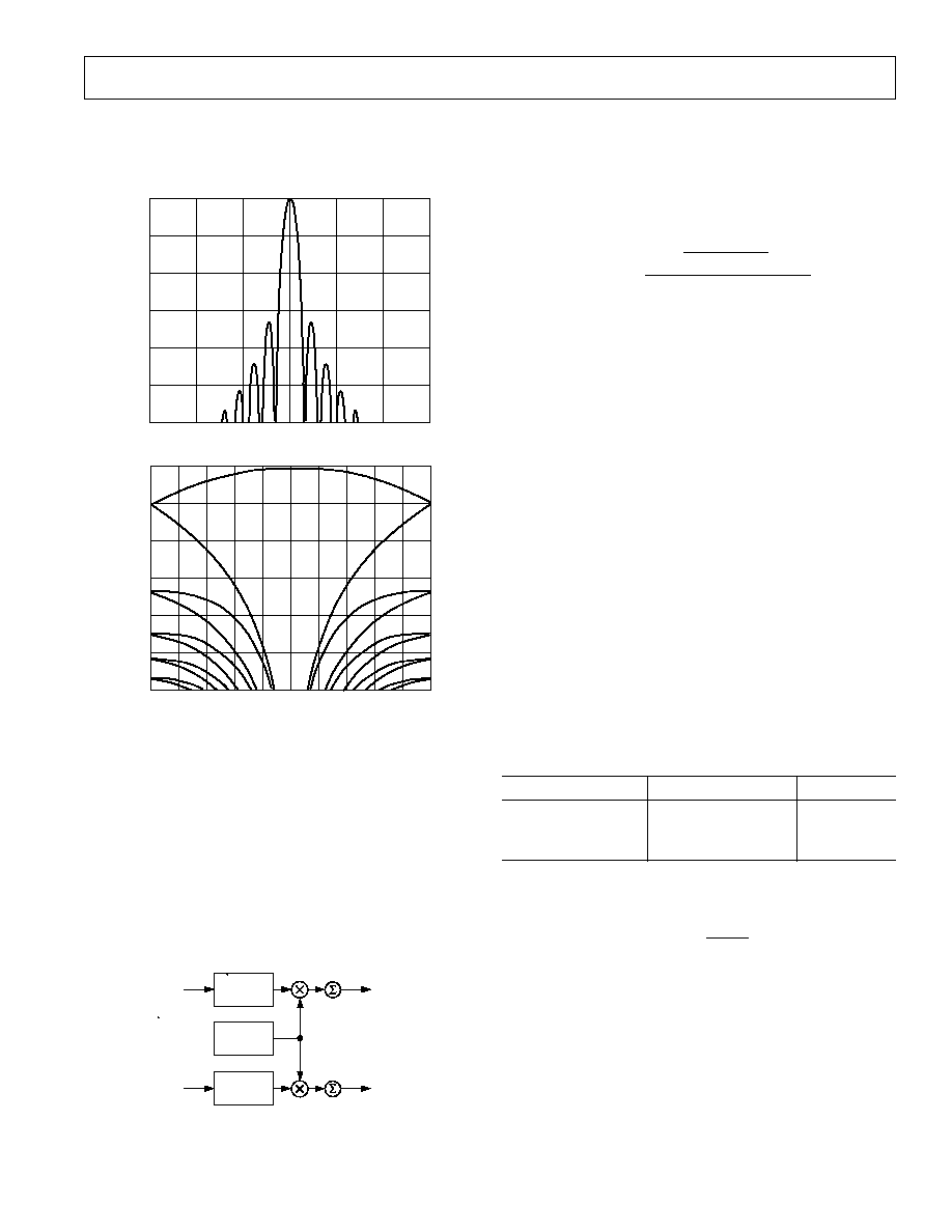
AD6620
25
REV. A
The maximum number of taps this filter can calculate, N
TAPS
, is
given by the equation below. The value N
TAPS
minus 1 is writ-
ten to the AD6620 internal address space at address 30C hex.
The decimation ratio of this filter, M
RCF
, may be programmed
from 1 to 32. The input rate into the RCF is f
SAMP5
. N
CH
is equal
to two for Diversity Channel Real Input mode; otherwise N
CH
= 1.
N
f
M
f
N
TAPS
CLK
RCF
SAMP
CH
×
min
,
5
256
The RCF coefficients are located in addresses 0x000 to 0x0FF
and are interpreted as 20-bit twos complement numbers. When
writing the coefficient RAM, the lower addresses will be multi-
plied by relatively older data from the CIC5 and the higher
coefficient addresses will be multiplied by relatively newer data
from the CIC5. The coefficients need not be symmetric and the
coefficient length, N
TAPS
, may be even or odd. If the coefficients
are symmetric, then both sides of the impulse response must be
written into the coefficient RAM.
The RCF stores the data from the CIC5 into a 256
× 36 RAM.
256
× 18 is assigned to I data and 256 × 18 is assigned to Q data.
The RCF uses the RAM as a circular buffer, so that it is difficult
to know in which address a particular data element is stored. To
avoid start-up transients due to undefined data RAM values, the
data RAM should be cleared upon initialization. The RCF
utilizes the number of data RAM locations equal to N
TAPS
× N
CH
,
rounded up to the nearest even number, starting from address
0x100, so these are the only values that need be cleared.
When the RCF is triggered to calculate a filter output, it starts
by multiplying the oldest value in the data RAM by the first
coefficient (located by the RCF
OFF
register in address 0x30B).
This value is accumulated with the products of newer data words
multiplied by the subsequent locations in the coefficient RAM
until the coefficient address RCF
OFF
+ N
TAPS
1 is reached.
Table V. Three-Tap Filter
Coefficient Address
Impulse Response
Data
0
h(0)
n(0) Newest
1
h(1)
n(1)
2 (N
TAPS
1)
h(2)
n(2) Oldest
The output rate of this filter is determined by the output rate of
the CIC5 stage and MRCF.
f
f
M
SAMPR
SAMP
RCF
=
5
RCF Coefficient Address Offset
This register at address 30b hex allows the AD6620 to hold
multiple filters in the RAM. However, the sum of the taps
required may not exceed 256 divided by the number of chan-
nels. The RCF will compute the filter from RCF_OFFSET to
(RCF_OFFSET + N
TAPS
). A single access can then be used to
select which of the filters is used without requiring coefficients
be rewritten.
The set of plots below (Figure 39) represents a decimation of 32
in the CIC5 filter. It can be seen that the lobes of the filter drop
as the decimation rate increases, but the aliased frequencies
increase due to the reduction of the output rate.
120
100
80
60
40
20
0
dBFS
f/f
SAMP
0.3
0.2
0.1
0.1
0.2
0.3
0
0.5
120
100
80
60
40
20
0
dBFS
f/f
SAMP5
0.4 0.3
0.2
0.1
0.1
0.2
0.3
0.4
0.5
0
Figure 39. CIC5 Alias Rejection, M
CIC5
= 32
RAM COEFFICIENT FILTER
The final signal processing stage is a sum-of-products decimat-
ing filter with programmable coefficients. Figure 40 shows a
simplified block diagram. The data memories I-RAM and Q-RAM
store the 256 most recent complex samples from the previous filter
stage with 18-bit resolution. The coefficient memory, C-RAM,
stores up to 256 coefficients with 20-bit resolution. On each
CLK cycle one tap for I and one tap for Q is calculated using
the same coefficients. The I and Q accumulators provide 3 bits
of headroom. This headroom allows the output of the RCF filter
to contain 23 significant bits.
I
IN
Q
IN
I
OUT
Q
OUT
256 18b
I-RAM
256 20b
C-RAM
256 18b
Q-RAM
Figure 40. RAM Coefficient Filter Block Diagram

AD6620
26
REV. A
RCF Output Scale Factor
The scale factor associated with the RCF, S
OUT
, behaves differ-
ently than the scale factors in the CIC stages. This scalar, at the
RCF output, controls the weight of the 16-bit output data going
to the parallel port or to the serial port when using 16-bit words.
S
OUT
determines which of the 23 RCF output bits are used
based on the equation below. OL
RCF
is the 23-bit RCF output
data; POL represents the output port data. POL is rounded to
the 16 bits desired. The weight of the rounding is adjusted by
S
OUT
. When the serial port is used with 24-bit or 32-bit words,
S
OUT
is ignored.
POL
round
OL
bits
RCF
S
OUT
=
×
16
4
2
(
)
(
)
Another way to consider the effects of the RCF Output Scale
factor is discussed here. If both CIC scalars follow the previous
recommendations, the following chart can be used to determine
what value to use for the RCF scale factor. In order to determine
this, the "gain" of the impulse response must first be determined.
This can be done by integrating the coefficients used for the
RCF filter remembering to normalize the values against the full-
scale input range of 2
19
.
There are several possibilities when setting the "gain" of the
RCF coefficients. Following these guidelines will preserve at
least three bits in the sum of products registers.
1.
h n
( )
=
1
; 0 dB dc gain in RCF filter. Numeric wraparound
very unlikely. The RCF Scale factor should be nominally
set to 4.
2.
h n
( )
1
; slight loss in RCF filter. Numeric wraparound
is impossible. The RCF Scale factor should be nominally
set to 4.
3.
h n
m
( )
=
; where the absolute value of m is a number less
than 1 and is scaled to account for losses elsewhere in the
system, such as conversion gain errors, attenuator losses or
CIC scaling errors. The gain should be scaled down to avoid
wraparound in the RCF process, however, then the RCF
Scale Factor can be adjusted up to increase the signal level.
The value of m can also be negative to account for an inver-
sion through an amplifier. The RCF Scale factor should be
set where needed to produce the desired full-scale results
with a fully loaded receiver input signal.
The RCF Scale factor has the effect as shown in the following
table. Each successive gain step doubles or halves the overall
gain of the stage. Overall gain through the RCF stage is the
cascaded gain of the RCF Scale factor shown below and the
RCF coefficient gain discussed previously.
Table VI.
RCF Gain
RCF Scale Factor (Address 309h)
1/8
7
1/4
6
1/2
5
1
4
2
3
4
2
8
1
16
0
Gain through the RCF of the AD6620 is thus:
Gain
Gain
coefficients
RCF
×
Unique B Operation
Unique B works in conjunction with dual channel mode. In this
mode, both the A and B channels can have different FIR coeffi-
cients. This can prove useful in many applications where each
signal path has known differences. Another option is that FIR
gain for one path could be different than the other. During
diversity selection, one path could be tailored for weak signals
and the other for strong signals, providing extra dynamic range.
To use the Unique B mode, set Bit 3 high in register 309h. This
will cause the internal state machine to use a different set of
coefficients for the B channel than the A. With Bit 3 set low for
normal operation, the FIR coefficient index is incremented only
after both the A and B channels are computed. However when
this bit is set high, the index is incremented after each A channel
and B channel computation. Therefore, filters are computed nor-
mally. When downloaded to the AD6620, they should be inter-
leaved with the A channel terms occupying the even RCF
Coefficient locations and the B channel terms occupying the
odd locations. Both filters must be the same length and fit in the
allocated memory space.
With Unique B set to `0,' the following table illustrates how the
coefficients are distributed.
Table VII.
Coefficient
Address
W(0)
0
W(1)
1
W(2)
2
W(3)
3
...
...
With Unique B set to `1,' the following table illustrates how the
coefficients are distributed.
Table VIII.
Coefficient
Address
Wa(0)
0
Wb(0)
1
Wa(1)
2
Wb(1)
3
...
...
AD6620
27
REV. A
If the AD6620s to be synchronized have identical decimation,
then latency through the filter stages will be matched and output
data rates for the Sync master's filter stages will match the cor-
responding filter stages of the slave.
SYNC M/S
MASTER
SLAVE
SYNC CIC
SYNC RCF
MASTER
SLAVE
Figure 42. SYNC_CIC, SYNC_RCF Pins
The three SYNC inputs to the control block originate from the
same three bidirectional pads from which the three SYNC out-
puts are driven. When the AD6620 is a SYNC MASTER, the
internal circuitry that generates the SYNC pulse outputs is
enabled to the pads. When the AD6620 is a SYNC SLAVE, the
internally produced SYNC pulses are three-stated, and the pads
are driven from an external input. The capacitance on these pins
must be closely monitored since the master responds to the
same SYNC pulse as the slave (its own pulse). There is no input
requirement to the relative phases of these SYNC pulses. In the
absence of SYNC pulses each state machine will free run so the
latter decimation filters can be reliably synchronized by the
SYNC pulses of an earlier stage. However, when sync pulses are
provided externally, setup-and-hold times must be met for each
respective input.
CONTROL REGISTERS AND ON-CHIP RAM
The AD6620 provides a choice of two control ports. It has an
8-bit generic microprocessor port that is used for configuring
the device at boot up and dynamically reconfiguring the AD6620
in the system. It also has a synchronous serial port that can also
dynamically reconfigure the AD6620 for the desired system
operation. All control registers are available from both the serial
port and the microprocessor port. These control methods are
nonexclusive and the two ports can be used simultaneously. If
simultaneous access occurs, the serial port is given precedence
over the microprocessor port unless a micro cycle is already
under way. The microprocessor port deasserts the RDY signal
and waits until the serial access is completed for Mode 0. The
microprocessor port does not assert DTACK for Mode 1 until
the serial access is completed.
Filter Phase Synchronization
Like the NCO, the AD6620 filter stages have phase synchroni-
zation circuitry enabling multiple AD6620s to be used in appli-
cations such as diversity antennas and phased array systems.
For any f
SAMP
, there are M
CIC2
possible phases of f
SAMP2
at the
output of the CIC2 stage. Similarly, at the output of the CIC5
stage, there are M
CIC5
possible phases of f
SAMP5
. This means that
at the output of the CIC stages there is already M
CIC2
× M
CIC5
possible phases of the filtered data. Additional phase uncertainty
is introduced by decimation done in the RCF. At the output of
the AD6620 there are a total of M
CIC2
× M
CIC5
× M
RCF
possible
output phases of the data.
In diversity systems using multiple AD6620s, it is necessary to
ensure that the output of each AD6620 in the system is in phase.
A variety of system issues (e.g., not bringing the AD6620s on
line at the same time, excessive digital noise) could cause the
AD6620s to start out-of-phase or to drift out-of-phase as the
system runs. To achieve output phase coherence in such systems
the SYNC_CIC and SYNC_RCF pins are provided.
The function of these pins is controlled by the SYNC_M/S bit
in the Mode Control Register at address 300 hex of internal
address space. When the SYNC_M/S bit is high, SYNC_CIC
and SYNC_RCF provide synchronization pulses on the rising
edge of CLK. When the SYNC_M/S bit is low, SYNC_CIC and
SYNC_RCF accept external synchronization pulses sampled on
the rising edge of clock. This pulse edge synchronizes the CIC2,
CIC5 and RCF filter stages of all AD6620 in the chain.
Below is an example of the output SYNC pulse waveforms.
The SYNC_NCO pulse is not shown and is described in the
preceding NCO Synchronization section. Each SYNC_RCF
output pulse is concurrent with a SYNC_CIC pulse. The
SYNC_RCF output pulse can be connected to the SYNC_CIC,
and SYNC_RCF inputs of another AD6620 to achieve full
decimation synchronization.
CLK
SYNC CIC
SYNC RCF
Figure 41. SYNC Output Pulses
In the example above, M
CIC2
= 3, and M
CIC5
= 1 as evidenced
by the SYNC_CIC pulses that occur every 3 CLK cycles
(M
CIC2
× M
CIC5
). M
RCF
= 3, resulting in SYNC_RCF pulses
that are one third as frequent as the SYNC_CIC pulses. In this
example full rate input timing is employed such that the input
data rate equals the clock rate.

AD6620
28
REV. A
Table IX. Control Register and RAM Addresses
Address
Bit Width
Name
Notation
Description
0000FF
20
RCF Coefficient RAM
RCF Coefficient RAM
1001FF
36
RCF Data RAM
RCF Data RAM
20027F
0
Reserved
Reserved
300
8
MODE CONTROL REGISTER
0: SOFT_RESET
1
1: Diversity Channel Real Input Mode
2: Single Channel Complex Input Mode
3: Sync Master/Slave
2
(Master = 1,
Slave = 0)
74: Reserved
301
3
NCO CONTROL REGISTER
0: NCO Bypass (Bypass = 1, Active = 0)
1: Enable Phase Dither
2: Enable Amplitude Dither
73: Reserved
302
32
NCO SYNC CONTROL REGISTER
SYNC_MASK
Write: Sync Mask Shadow
Read: Sync Mask
303
32
NCO_FREQ
NCO_FREQ
Channel Frequency for NCO Tuning
304
16
NCO PHASE_OFFSET
NCO Phase Offset
305
8
INPUT/CIC2 SCALE REGISTER
20: S
CIC2
3: Reserved
4: ExpInv
75: : ExpOff
306
8
M
CIC2
1
M
CIC2
1
CIC2 Decimation Minus One
307
5
CIC5 SCALE REGISTER
S
CIC5
40: S
CIC5
75: Reserved
308
8
M
CIC5
1
M
CIC5
1
CIC5 Decimation Minus One
309
4
OUTPUT/RCF CONTROL REGISTER
S
OUT
20: Output Scale Factor
3: Unique B Flag (Normal Mode = 0,
Unique B Mode = 1)
74: Reserved
30A
8
M
RCF
1
M
RCF
1
RCF Decimation Minus One
30B
8
RCF ADDRESS OFFSET REGISTER
RCF
OFF
Filter Coefficient Address Offset
30C
8
N
TAPS
1
N
TAPS
1
Number of Taps Minus One
30D
8
Reserved (Should Be Written 0)
Reserved (Should Be Written 0)
NOTES
1
This bit is set high on
RESET. The chip is held into SOFT_RESET until it is written low.
2
This bit is set low on
RESET. This keeps multiple AD6620 SYNC Masters from driving each other.
outputs while acting as a sync master, or as inputs while acting
as a sync slave. This is the only register with a defined power-up
state: on power-up, Bit 0 will be at a Logic "1." This places the
chip in SOFT_RESET and defines the chip as a sync slave.
Powering up as a sync slave avoids contention problems when
connecting multiple AD6620s.
If Bit 0 is written low and Bits 2 and 1 are low, the AD6620 is in
Single Channel Real Mode. If Bit 1 is high and Bits 0 and 2 are
low, the device is in the Diversity Channel Real Mode. If Bit 2
is high and Bits 0 and 1 are low, the chip is in the Single Chan-
nel Complex Mode. Setting Bit 3 high configures the AD6620
as a SYNC master; the SYNC pins are then used as outputs. If
Bit 3 is low, it is a SYNC slave and the SYNC pins function
as inputs. Bits 74 are reserved and should be written low.
(0x301) NCO Control Register
This register allows control of special features of the NCO. If
Bit 0 of this register is high the NCO of the AD6620 is by-passed.
Both the I data and the Q data that are passed through the chip
will be the same and the Spectrum will not be translated. In
bypass the input data is attenuated by 12 dB.
(0x0000xFF) RCF Coefficient RAM
Memory that stores user-programmable coefficients for the RCF
filter. The RAM will hold 256 20-bit twos complement words
for a maximum filter length of 256 taps. In Diversity Channel
Real Mode the filter length is limited to 128 taps per channel.
The number of taps used is controlled by N
TAPS
1 (30C) regard-
less of the number of coefficient locations programmed. If filter
size allows, more than one filter can be resident in the memory
at a time. This makes it possible to switch filters without reloading
all of the coefficients.
(0x1000x1FF) RCF Data RAM
These locations store I and Q data exiting the CIC5 filter stage
while the RCF performs multiply accumulates. The lower 18
bits of the 36-bit location is I data; the upper 18 bits are Q data.
These locations are addressed in memory and are available via
the control ports so that the data RAM can be flushed for test-
ing and simulation purposes. They are not cleared on reset.
(0x300) Mode Control Register
This location brings the chip out of reset and sets the operating
mode. It also specifies how the chip will use its SYNC pins: as

AD6620
29
REV. A
(0x309) Output/RCF Control Register
Bits 2-0 of this register hold the Output Scale Factor, S
OUT
.
These bits are interpreted as a 3-bit unsigned integer, the value
of which controls which of the 23 output bits of the RCF are
passed to the output port being used. The data output corre-
sponds to the following equation where OL
RCF
is the 23-bit
output of the RCF and POL is the 16-bit data available at the
parallel output port or the serial port when 16-bit serial words
are used. The truncation function rounds the scaled 23-bit
number to 16 bits. S
OUT
is ignored when WL is 24 or 32 bits. In
most applications, this register should be set to 4 as an initial
starting value.
POL
round
OL
bits
RCF
S
OUT
=
×
16
4
2
(
)
(
)
For additional details on determining RCF gain, see the RCF
Output Scale Factor section.
Bit 3 of this register is used to control the Unique B feature of
the chip. When written low, the normal mode, the chip uses the
same FIR coefficients for both the A and B channels. However,
when the bit is set high, different coefficients are used for the A
and B channels. When Unique B mode is selected, the filter
coefficients should be interleaved with the A channel terms
occupying the even RCF Coefficient locations and the B chan-
nel terms occupying the odd locations.
Bits 74 of this register are reserved and must be written 0.
(0x30A) (M
RCF
1)
This register controls the amount of decimation in the RCF
filter stage. The value contained in this register is the RCF
decimation rate minus one. This is interpreted as an unsigned
8-bit integer, but due to limited number of taps and, therefore,
filtering power in the RCF filter accumulators this value should
be limited to 31 (decimation = 32).
(0x30B) RCF Address Offset Register
This register controls the address offset used by the RCF to
calculate a given filter and is interpreted as an 8-bit unsigned
integer. It allows more than one filter to be placed in the Coeffi-
cient RAM. This makes it possible to switch filters without
reloading all of the coefficients. The RCF filter will compute
taps for all coefficients between RCF
OFF
and (RCF
OFF
+ N
TAPS
)
provided that the decimation, CLK rate and input data rate
provide sufficient time for this.
(0x30C) (N
TAPS
1)
This register controls the number of taps calculated by the RCF.
The value in this register is interpreted as an unsigned integer
and is equal to the number of taps desired minus one. This filter
is not inherently symmetric and the number of coefficients placed
in the Coefficient RAM will be equal to the number of taps,
provided that only one filter at a time is loaded. No symmetry is
assumed and preaddition is not used. The total number of taps
for all filters must be less than 256 taps for Single Channel
Real mode, or less than 128 taps/channel for Diversity Channel
Real mode.
(0x30D) Reserved
Reserved, but must be written 0 for correct operation.
The NCO has two features to improve the performance of some
systems: Phase Dither and Amplitude Dither. These can be used
together or alone. If Bit 1 of the register is high, Phase Dither is
activated. If Bit 2 is high, Amplitude Dither is activated. For
more information on dither refer to the NCO section.
(0x302) NCO SYNC Control Register
This holds the SYNC_MASK, which controls the frequency of
the SYNC_NCO pulses and therefore the phase accuracy of the
synchronization. See the NCO section for details.
(0x303) NCO_FREQ
This register holds the NCO frequency control word as described
in the NCO section. This is a 32-bit unsigned integer that sets
the frequency of the AD6620 NCO.
(0x304) NCO PHASE_OFFSET
This register controls the phase offset of the NCO. It is also
described in detail in the NCO section and can be used to allow
for phase differences between multiple antennas receiving the
same carrier.
(0x305) INPUT/CIC2 Scale Register
This register holds the scale factor, S
CIC2
, for CIC2. S
CIC2
scales
down the data before it is accumulated in CIC2. This avoids
register wrap-around in the twos-complement arithmetic and
eliminates the resulting spectral errors. S
CIC2
is contained in Bits
20 of this register. It is treated as an unsigned integer between
0 and 6. Increasing S
CIC2
shifts data down. For more details
refer to the section on the CIC2 filter.
The second function of this register is to scale the input data
from the Parallel Data Input port. This allows the AD6620 to
treat the floating point input data with considerable flexibility.
There are two parts of this function. The first is Bit 4, which
tells the AD6620 how to handle the exponent, EXP[2:0]. If this
bit is low, data is shifted down as the exponent increases. If this
bit is high, then for increasing EXP[2:0] the input data is shifted
up. The second part of the input data shifting is the Exponent
Offset(ExpOff[7 . . 5]) held in Bits 75 of this register. This pro-
vides gain to the input data as described in the Input Port section.
(0x306) (M
CIC2
1)
This register controls the amount of decimation in the CIC2 filter
stage. The value contained in this register is the CIC2 decima-
tion rate minus one. This is interpreted as an unsigned 8-bit
integer but due to limited growth in the CIC2 filter accumula-
tors this value should be limited to 15 (decimation = 16).
(0x307) S
CIC5
This register holds the scale factor, S
CIC5
, for CIC5. S
CIC5
scales
down the data before it is accumulated in CIC5. This avoids
register wrap-around in the twos-complement arithmetic and elimi-
nates the resulting spectral errors. S
CIC5
is contained in Bits 40
of this register. It is treated as an unsigned integer between 0
and 20. Increasing S
CIC5
shifts data down. For more details refer
to the section on the CIC5 filter.
(0x308) (M
CIC5
1)
This register controls the amount of decimation in the CIC5
filter stage. The value contained in this register is the CIC5
decimation rate minus one. This is interpreted as an unsigned
8-bit integer, but due to limited growth in the CIC5 filter accu-
mulators this value should be limited to 31 (decimation = 32).

AD6620
30
REV. A
PROGRAMMING THE AD6620
Initializing the AD6620
Before the AD6620 can be used to down convert and filter the
channel of interest it must be configured for the job. First the
RESET pin should be pulsed low for a minimum of 30 ns and
should then be returned high. This HARD_RESET of the
AD6620 clears the CIC Accumulators as well as the NCO
Phase Accumulator. When
RESET is brought high the AD6620 is
removed from the HARD_RESET condition. The AD6620 is
now in SOFT_RESET. In this state the Mode Control Register
at address 0x300 contains a "1" (Bit 0 is high). When the AD6620
is in SOFT_RESET, no data is accepted by the input data port
and no processing occurs. The serial port and parallel output
port is held inactive and the chip is defined as a SYNC slave to
avoid possible contentions on these pins. While the AD6620 is
in this condition it should be programmed by the process below.
It should be noted that this initialization must be performed via
the microprocessor port since the serial port is inactive.
1. If the AD6620 is being reinitialized without performing a
HARD_RESET, then address 0x300 should be written 1 to
place the AD6620 in SOFT_RESET. This allows the non-
dynamic registers to be programmed.
2. Program the Coefficient RAM of the AD6620 with the
desired FIR Filter. The address auto-increment feature can
be used to decrease the amount of time required to program
the Coefficients. This feature is described in detail in the
Microport Control section that follows.
3. (Optional) The first piece of data out of the AD6620 is always
zero due to an output pipeline delay. There will also be a
start-up glitch on the output of the AD6620 due to possible
nonzero data in the I and Q data RAMS of the RCF filter.
These RAMS are not initialized by the HARD_RESET. If
this is a concern then the data RAMS should now be written
to zero. For efficiency the auto-increment feature can be
used as with the programming of the coefficient RAMs.
4. The Configuration Registers of the AD6620 are now pro-
grammed. First, address 0x300 should be written to set the
Operating Mode if Diversity Channel Real or Single Channel
Complex Modes are used. Bit 0 of this register should remain
high at this time. This will hold the SOFT_RESET condition.
The remaining configuration registers can now be programmed.
This should start at address 0x301 and continue to address
0x30D. This defines the operation of the NCO and filter stages.
5. The AD6620 is now ready to be removed from SOFT_RESET
and allowed to process data. This is done by writing address
0x300 to again set the desired mode of operation. This loca-
tion should be set for SYNC MASTER or SYNC SLAVE
operation at this time. Bit 0 of this register is written low at
this time to remove the SOFT_RESET condition.
Dynamic Programming of the AD6620
Many attributes of the AD6620 may be altered dynamically as
the AD6620 processes the received data. This allows the receiver
to be adjusted during operation in order to achieve the maxi-
mum performance. The typical dynamic registers of the AD6620
are listed in the following table. To program the other registers
follow the steps described in the section titled Initializing the
AD6620. Technically all registers can be programmed dynami-
cally, but adverse results may occur if registers other those listed
are written dynamically.
These addresses may be programmed via either the Micropro-
cessor or the Serial Control Ports.
Table X. Dynamic AD6620 Registers
Address
Bit Width
Name
302
32
NCO SYNC CONTROL REGISTER
303
32
NCO_FREQ
304
16
NCO PHASE_OFFSET
305
8
INPUT/CIC2 SCALE REGISTER
307
5
CIC5 SCALE REGISTER
309
4
OUTPUT/RCF CONTROL REGISTER
30B
8
RCF ADDRESS OFFSET REGISTER
Registers 0x302, 0x303 and 0x304 allow the NCO of the AD6620
to be adjusted. The tuning frequency can be dynamically changed
for frequency hopping. The phase of the carrier can be adjusted
with address 0x304. The phase accuracy of the synchronization
can be changed with 0x302. Registers 0x305, 0x307, and 0x309
allow the user to dynamically control the gain of the AD6620 in
6 dB increments. This can be used to maximize the AD6620s
dynamic range for the signal being tuned at a particular instant.
Register 0x307 allows for AGC where the DSP does power
spectral estimation.
In addition to dynamically writing to these registers, they may
also be read to verify program content. Care should be taken,
however, because reading some registers may affect normal chip
operation. In particular, reading from 303h the NCO frequency
will cause the phase accumulator to be reset via the SYNC_NCO
pulse if the AD6620 is running as a Sync master. If the device is
run as a Sync slave, then the phase accumulator is not reset.
Addresses 000h through 1FFh should not be read dynamically
as doing so will disrupt the internal state machine computing
the FIR taps. These locations may be read statically if needed.

AD6620
31
REV. A
ACCESS PROTOCOLS
The AD6620 external accesses may be performed through either
the Microprocessor Port or the Serial Port. The Microport and
the serial port both use a three-bit address and eight-bit data to
access these registers. The three-bit address provides access to
seven register locations (External Interface Registers). These
register locations are used to access the internal address space of
the AD6620 shown in the Control Register section. The seven
registers are the LAR (Low Address Register), the AMR (Address
Mode Register), and the five data registers (DR4DR0).
Table XI. External Interface Registers
A[2:0]
Name
Comment
000
Data Register 0 (DR0)
D[7:0]
001
Data Register 1 (DR1)
D[15:8]
010
Data Register 2 (DR2)
D[23:16]
011
Data Register 3 (DR3)
D[31:24]
100
Data Register 4 (DR4)
D[35:32]
101
Reserved
Reserved
110
Low Address Register (LAR)
A[7:0]
111
Address Mode Register (AMR)
1-0: A[9:8]
5-2: Reserved
6: Read Increment
7: Write Increment
The internal address space is accessed using a 10-bit internal
address. Many of these address locations are more than a byte
wide and require multiple accesses to the seven External Inter-
face Registers, which are each only 8 bits wide (only 4 bits of
DR4 are used). Accesses to these registers are accomplished
using the 3-bit address and 8-bit data lines the manner described
below. The source of these values depends on the control port
method used.
All internal accesses are accomplished by first writing the inter-
nal address of the register or memory location to be accessed.
The lower eight address bits are written to the LAR register
and the upper two address bits to the LSBs of the AMR. This
defines the internal address of the location to be accessed as
shown in the memory map shown in the Control Registers and
On-Chip RAM section.
Internal Write Access
Up to 36 bits of data (as needed) can be written by the process
described below. Any high order bytes that are needed are writ-
ten to the corresponding data registers defined in the external
3-bit address space. The least significant byte is then written to
DR0 at address (000). When a write to DR0 is detected, the
internal microprocessor port state machine then moves the data
in DR4DR0 to the internal address pointed to by the address
in the LAR and AMR.
Write Pseudocode
void write_micro(ext_address, int data);
main();
{
/
* This code shows the programming of the NCO frequency
register using the write_micro function as defined above. The
variable address is the External Address A[2:0] and data is the
value to be placed in the external interface register. The NCO
register is located at Internal Address = 0x303
*/
// holding registers for NCO byte wide access data
int d3, d2, d1, d0;
// NCO frequency word (32-bits wide)
NCO_FREQ = 0xCBEFEFFF;
// write AMR
write_micro(7, 0x03);
// write LAR
write_micro(6, 0x03);
// DR4 is not needed because NCO_FREQ is only 32-bits, not
36
// write DR3 with high byte of 32 bit word (D[31:24]
d3 = (NCO_FREQ & 0xFF000000) >> 24;
write_micro(3, d3);
// write DR2 with high byte of 32 bit word (D[23:16]
d2 = (NCO_FREQ & 0xFF0000) >> 16;
write_micro(2, d2);
// write DR1 with D[15:8]
d1 = (NCO_FREQ & 0xFF00) >> 8;
write_micro(1, d1);
// write DR0 with D[7:0]
// Writing to DR0 causes all data to be transferred to the
internal address.
//Therefore, DR1, DR2 and DR3 should already be written
d0 = NCO_FREQ & 0xFF;
write_micro(0, d0);
} // end of main
Internal Read Access
A read is performed by first writing the LAR and AMR as with a
write. The data registers (DR4DR0) are then read in the reverse
order that they were written. First, the least significant byte of
the data (D[7:0]) is read from DR0. On this transaction the
high bytes of the data are moved from the internal address
pointed to by the LAR and AMR into the remaining data regis-
ters (DR4DR1). This data can then be read from the data
registers using the appropriate 3-bit addresses. The number of
data registers used depends solely on the amount of data to be
read or written. Any unused bit in a data register should be
masked out for a read.

AD6620
32
REV. A
Read Pseudocode
int read_micro(ext_address);
main();
{
/
* This code shows the reading of the NCO frequency register
using the read_micro function as defined above. The variable
address is the External Address A[2..0] and data is the value to
be placed in the external interface register. The NCO register is
located at Internal Address = 0x303.
*/
// holding registers for NCO byte wide access data
int d3, d2, d1, d0;
// NCO frequency word (32-bits wide)
// write AMR
write_micro(7, 0x03 );
// write LAR
write_micro(6, 0x03);
/
* read D[7:0] from DR0, All data is moved from the Internal
Registers to the interface registers on this access. Reading
should be initiated with a read from DR0. Therefore, DR1,
DR2 and DR3 can be read after DR0
*/
d0 = read_micro(0) & 0xFF;
// read D[15:8] from DR1
d1 = read_micro(1) & 0xFF;
// read D[23:16] from DR2
d2 = read_micro(2) & 0xFF;
// read D[31:24] from DR3
d3 = read_micro(3) & 0xFF;
// DR4 is not needed because NCO_FREQ is only 32-bits
// Assemble 32-bit NCO_FREQ word from the 4 byte
components
NCO_FREQ = d0 + (d1 << 8) + (d2 << 16) + (d3 << 24);
} // end of main
Auto Increment Feature
To increase throughput, an auto increment feature is provided.
This feature is controlled by Bits 6 and 7 of the AMR. If these
bits are set to 00, the address remains the same after an internal
access. If set to 01, the address is incremented after a read access
has been performed. If set to 10, the address is incremented
after a write access is performed. If set to 11, the address is incre-
mented after each access, read or write. This allows the AD6620
to be initialized in a much shorter time since the access to the
LAR and AMR must occur only once to initialize or read-back
the entire device.
MICROPORT CONTROL
External reads and writes are accomplished in one of two modes
via the Microprocessor Port. The
CS, RD (DS), RDY (DTACK),
WR (R/W) and MODE pins are used to control the access. The
specific function of these pins depends on whether the access is
MODE 0 or MODE 1. The Mode 1 signal names are those
listed on the pinout. The access mode is controlled by the
MODE input as described in the following sections.
Table XII. Microprocessor Control Signals
MODE 0
MODE 1
A[2:0] (Address Lines)
A[2:0] (Address Lines)
D[7:0] (Data Lines)
D[7:0] (Data Lines)
CS (Chip Select)
CS (Chip Select)
RD (Read Strobe)
DS (Data Strobe)
WR (Write Strobe)
R/W (Read/Write Select)
RDY (Ready Signal)
DTACK (Data Acknowledge)
MODE (Mode Select)
MODE (Mode Select)
The Microport is synchronous with the master clock (CLK) of
the AD6620, but the interface is not required to be. If the speed
of the interface is significantly slower than CLK, synchronicity
should not be an issue. If the interface is relatively fast com-
pared to CLK, the user may need to synchronize the Microport
to CLK or add wait states to the controlling processor. The
timing diagrams show the relationship of the control signals to
clock and the user should use these as a guide to implement a
Microport interface.
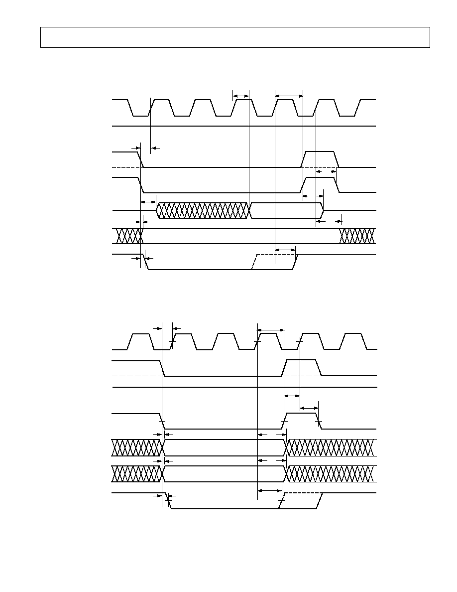
AD6620
33
REV. A
Mode = 0
If MODE is low during the access, the interface is in Mode 0.
In Mode 0 the
CS, RD and the WR lines control the access
type. While an access is being performed, or if the serial port
DATA VALID
t
HC
t
SC
t
HC
t
SC
t
HM
ADDRESS VALID
N
N+1
N+2
N+3
N*
CLK
1
WR
2
RD
2
CS
3
D[7:0]
RDY
A[2:0]
NOTES:
1
RDY IS DRIVEN LOW ASYNCHRONOUSLY BY
WR AND CS GOING LOW AND RETURNS HIGH ON THE
2
THESE SIGNALS (R/W AND
DS) MAY REMAIN IN LOW STATE TO CONTINUE WRITING DATA.
3
CS MUST RETURN TO HIGH STATE AND BE SAMPLED BY CLK (N+3 SHOWN) TO COMPLETE WRITE.
*THE NEXT WRITE MAY BE INITIATED ON CLK, N.
t
HA
t
RDYH
t
RDYL
t
SAM
t
SAM
RISING EDGE OF CLK "N+2".
Figure 44. Mode 0 Write (MODE = GND)
is accessing the chip, the RDY line goes low at the start of
the access. When the internal cycle is complete the RDY line
is released.
t
DD
DATA VALID
t
HC
t
SC
t
HC
t
ZD
t
HA
t
RDY
t
RDY
ADDRESS VALID
t
SAM
t
ZR
N
N+1
N+2
N+3
N+4
N
CLK
1
WR
2
RD
2
CS
3
D[7:0]
RDY
1
A[2:0]
NOTES:
1
RDY IS DRIVEN LOW ASYNCHRONOUSLY BY
RD AND CS GOING LOW AND RETURNS HIGH ON THE RISING EDGE
OF CLK "N+3" FOR INTERNAL ACCESS (A[2:0] = 000), CLK "N+2" OTHERWISE.
2
THE SIGNAL,
WR, MAY REMAIN HIGH AND RD MAY REMAIN LOW TO CONTINUE READ MODE.
3
CS MUST RETURN TO HIGH STATE AND BE SAMPLED BY CLK (N+4 SHOWN) TO COMPLETE READ.
Figure 43. Mode 0 Read (MODE = GND)
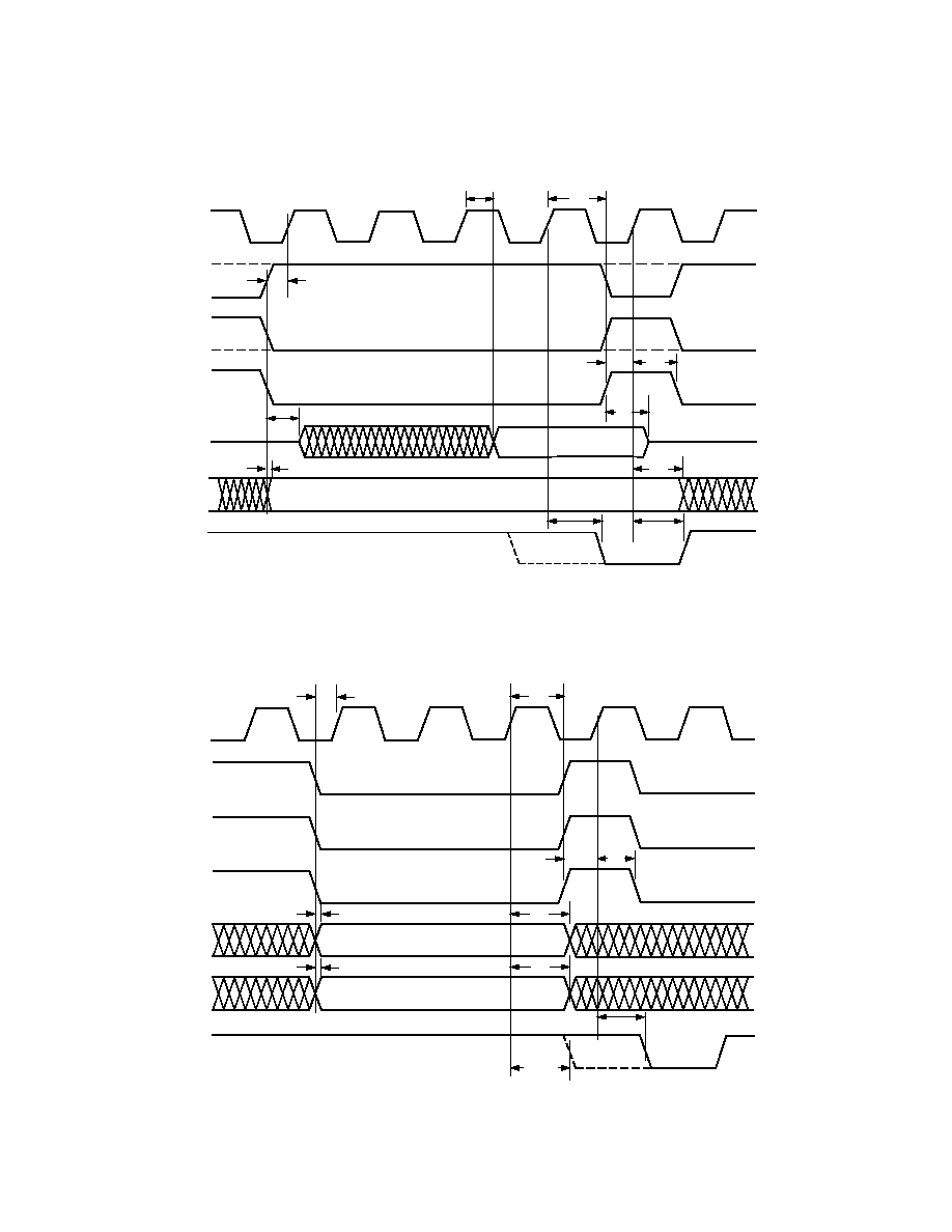
AD6620
34
REV. A
DATA VALID
t
SC
ADDRESS VALID
N
N+1
N+2
N+3
CLK
1
R/W
2
DS
2
CS
3
D[7:0]
DTACK
A[2:0]
t
SAM
N+4
N
t
HC
t
DD
t
HC
t
ZD
t
HA
t
DTACK
t
DTACK
NOTES:
1
DTACK IS DRIVEN LOW ON THE RISING EDGE OF CLK "N+3" FOR INTERNAL ACCESS (A[2:0] = 000),
CLK "N=2" OTHERWISE.
2
THE SIGNAL, R/W MAY REMAIN HIGH AND
DS MAY REMAIN LOW TO CONTINUE READ MODE.
3
CS MUST RETURN TO HIGH STATE AND BE SAMPLED BY CLK (N+4 SHOWN) TO COMPLETE ACCESS
AND FORCE
DTACK HIGH.
t
SC
t
ZR
Figure 45. Mode 1 Read (MODE = VDD)
Mode = 1
If the MODE input is held high the interface is in Mode 1. In
Mode 1 the
RD signal becomes the data strobe (DS) and the
WR signal becomes a read/write (R/W) select signal. In this
t
SC
N
N+1
N+2
N+3
t
SAM
N*
t
DTACK
t
SC
CLK
1
R/W
2
DS
2
CS
3
D[7:0]
DTACK
A[2:0]
t
HC
t
HC
t
DTACK
t
SAM
t
HM
t
HA
NOTES:
1
ON RISING EDGE OF "N+3" CLK,
DTACK IS DRIVEN LOW.
2
THESE SIGNALS (R/W AND
DS) MAY REMAIN IN LOW STATE TO CONTINUE WRITING DATA.
3
CS MUST RETURN TO HIGH STATE AND BE SAMPLED BY CLK (N+3 SHOWN) TO COMPLETE WRITE
AND FORCE
DTACK HIGH.
*THE NEXT WRITE MAY BE INITIATED ON CLK, N*
DATA VALID
ADDRESS VALID
Figure 46. Mode 1 Write (MODE = VDD)
mode the
DTACK signal goes low when data is available during
a read or when data has been latched during a write. The
DTACK
signal stays low until the
DS signal is released.
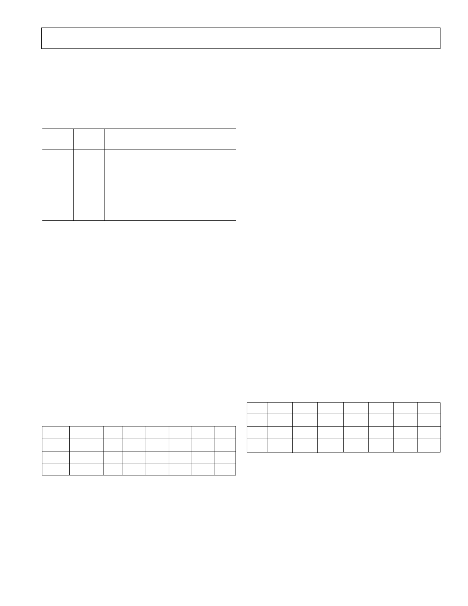
AD6620
35
REV. A
The data is contained in the low byte of the 16 significant bits.
This data will be placed into the external interface register
pointed to by A[2 . . 0] for a write and will be ignored for a read.
Serial Port Writes
If the WRITE bit is high and the READ bit is low then a write
access is performed to the external interface register pointed to
by A[2 . . 0]. A write to an internal register takes place by first
writing the AMR and LAR. The data registers DR4DR1 are
then written as needed. A final write to DR0 then moves the
data to the internal register.
Serial Port Reads
If the READ bit is high, then a read to the register indicated is
performed and the data will appear in the RDATA word appended
to the serial frame. The internal data read is loaded into the
serial data word in FIFO fashion. The first byte read is loaded
into the first eight bits, the second read during the frame is
loaded into the second byte, etc. Since the serial data is shifted
MSB first, the first byte will actually be loaded into the most
significant byte of the serial data word.
During a frame (the period between SDFS rising edges) up to
four reads may occur. When a read is requested through the
serial port, a data word is appended to the end of the serial string.
Even if AD is not asserted (see below for AD description) a word is
added to the end of the IQ data stream. Therefore, if the chip is
in single channel mode, the I and Q data are sent followed by a
read word. If the chip is in diversity channel mode, the IQ pairs
are followed by a read word. Thus the serial port responds with
either three or five serial words in a frame, respectively. If AD is
asserted, the read word is sent each frame regardless of a request. If
no requests are made, the appended word is all zeros.
The number of reads accomplished in a frame is limited by the
serial word length. If the serial word length is 16 bits, only two
reads can be performed during a frame. If the serial word length
is 24 bits, three reads can occur in a frame. If the serial word
length is 32 bits, then up to four reads can occur in a frame.
The RDATA word format is shown below. Rows three and four
will not be present when 16-bit words are used, and row four
will not be present when 24-bit words are used.
Table XV. RDATA Word Definition
DA7
DA6
DA5
DA4
DA3
DA2
DA1
DA0
DB7
DB6
DB5
DB4
DB3
DB2
DB1
DB0
DC7
DC6
DC5
DC4
DC3
DC2
DC1
DC0
DD7
DD6
DD5
DD4
DD3
DD3
DD1
DD0
The number of words in the serial frame depends on the operat-
ing mode of the chip (one or two I/Q pairs) and whether or not
a read access occurs. It also depends on the Append Data pin,
AD. When this signal is asserted, then the RDATA word is
appended to the Serial Frame regardless of whether or not a
read was performed in the frame. This allows time-slotted sys-
tems where multiple AD6620s or other devices share a serial
port of a DSP without hardware handshakes. When AD is
high and there has not been a read during the active frame,
the RDATA word is driven low and SDFE is held off for another
serial word length.
At all times, the serial interface must have time to shift all bits.
The section below Serial Port Guidelines should be consulted to
determine if sufficient time exists.
SERIAL PORT CONTROL
In addition to providing access to the complex output data stream
of the AD6620, the Serial Port can also be used for Dynamic
Control of the device. The dynamic registers of the AD6620
that are typically programmed while the chip is processing are
listed in the table below. In order to use the serial port control,
the chip must first be booted using the microprocessor interface.
Table XIII. Dynamic Registers
Bit
Address
Width
Name
300
8
MODE CONTROL REGISTER
302
32
NCO SYNC CONTROL REGISTER
303
32
NCO_FREQ
304
16
NCO PHASE_OFFSET
305
8
INPUT/CIC2 SCALE REGISTER
307
5
CIC5 SCALE REGISTER
309
4
OUTPUT/RCF CONTROL REGISTER
30B
8
RCF ADDRESS OFFSET REGISTER
The internal address and data structure are shared between
the microprocessor port and the serial port. When accessing
the internal RAM or registers, the serial port is given priority
over a microprocessor request. If a Mode 0 access occurs on
the microport while the serial port is accessing the internal address
space, the RDY line will go low and stay low until the serial
access has been completed. If a Mode 1 access occurs on the
microport during a serial access, the
DTACK signal will not go
low until the serial access has been completed. The microport is
used for booting the AD6620 and either the microport or the
serial port can be used to dynamically change the system param-
eters. Both ports may be used in the same design provided that
the handshaking rules described above are observed.
For each word shifted out of the serial port there is a word
shifted in. Each input word can provide one internal access. Each
access can be a read or a write. All reads and writes are per-
formed via the same 8-bit registers used by the microprocessor
port. Each bit in the SDI words has a predefined meaning and
are used to decode which of these registers are being accessed
and whether the access is a read or a write. The bits are defined
according to the table below.
Table XIV. SDI Input Word Definition
READ
WRITE
x
x
x
A2
A1
A0
D7
D6
D5
D4
D3
D2
D1
D0
x
x
x
x
x
x
x
x
x
x
x
x
x
x
x
x
Only the first 16 bits of the SDI word contain significant data
regardless of the serial word length. The first two bits shifted in
are the READ and WRITE indicator signals. These bits control
the access type as described below and should not be asserted
simultaneously. If the Serial Port is not used for control then the
SDI pin should be tied low to disable register reads and writes.
The three address bits are the three least significant bits of the
upper byte in the 16-bit word. These three bits A[2:0] define
which of the seven external registers are accessed by the serial
port according to Table XI.

AD6620
36
REV. A
Example of Serial Port W/R Operation
The example shown below demonstrates writing and reading
from the AD6620. For this example, the chip is set up in diver-
sity channel real mode. Therefore, there four data words (two Is
and two Qs) are generated as receiver data. Thus four commands
can be shifted into the SDI port. These are shown below. Addi-
tionally, the chip is configured with a word length of 16 bits.
The AD6620 response with five words per frame (two Is, two
Qs and the appended read word).
Table XVI. SDI Data Format
A-I
A-Q
B-I
B-Q
Append
SDO
XXXX
XXXX
XXXX
XXXX
0AXX
SDI
4703
4600
80XX
4603
XXXX
The table above shows the serial output bits for this configura-
tion. As the I and Q data are being shifted out, the SDI pin is
telling the chip what data to return during the appended data
field. During the A-I portion of the frame, the hex word 4703 is
shifted into the chip. Breaking this word down, the command
instructs the AD6620 to write an `03' into the AMR register.
The next word, 4600, writes a `00' into the LAR. Therefore, the
chip is so configured that the next command will either read
from or write to internal memory space `300' hex, the Mode
Control Register. The next word on the SDI pin is 80XX. This
indicates a read from DR0. Note that the second half of the read
word is ignored. During the B-Q word, another read or write
can be set up. In this case, 4603 changes the internal memory to
point to `303,' the NCO frequency, thus setting up subsequent
access of this register. Now during the append data frame, the
AD6620 sends any read words that are pending due to read
requests. In this case, the contents of register `300.' Since the
chip is in single channel complex mode and running, the chip
responds with `0AXX.' `0A' indicates that the chip is in diver-
sity channel real mode and running as a Sync master. The `XX'
is indeterminate and would have been the results of a second
read if one had been requested.
PAR/SER
The Serial Port shares pins with a Parallel Output Port. These
pins are arbitrated by the PAR/SER pin. In order to operate the
chip with the Parallel Output Data Port PAR/SER must be high
while
RESET is brought high. For Serial Port operation, PAR/
SER must be held low while
RESET is brought high. PAR/SER
should remain valid while the AD6620 is processing (should
only be changed in
RESET). PAR/SER should be hardwired on
a given design.
SBM
Serial Bus Master. When SBM is high, the AD6620 generates
SCLK and SDFS. When SBM is low, the AD6620 accepts
external SCLK and SDFS signals. When configured as a bus
master the SCLK signal can be used to strobe data into the DSP
interface. When used with another AD6620 in Serial Cascade
Mode, SCLK can be taken from the master AD6620 and used
to shift data out from the cascaded device. In this situation SDFS
of the Cascaded AD6620 is connected to the SDFE pin of the
master AD6620. When an AD6620 is in Serial Cascade Mode,
all of the serial port activities are controlled by the external
signals SCLK and SDFS.
Regardless of whether the chip is a Serial Bus Master or is in
Serial Cascade Mode, the AD6620 Serial Port functions are
identical except for the source of the SCLK and SDFS pins.
SCLK
SCLK is an output when SBM is high; SCLK is an input when
SBM is low. In either case the SDI input is sampled on the
falling edge of SCLK, and all outputs are switched on the rising
edge of SCLK. The SDFS pin is sampled on the falling edge of
SCLK. This allows the AD6620 to recognize the SDFS in time
to initiate a frame on the very next SCLK rising edge. The maxi-
mum speed of this port is 33.5 MHz or half of the master CLK
signal, whichever is lower. Care should be taken with this signal.
Even when the AD6620 is selected as a serial bus master, reflec-
tions on this line will cause the output shifters to `double shift'
output data causing corrupt serial data. If this signal is going to
a back plane of more than several inches, the line should either
be buffered or be matched to the impedance of the back plane.
See the Applications section of this data sheet for information
on driving the transmission lines.
SDI
Serial Data Input. Serial Data is sampled on the falling edge of
SCLK. This pin is used to write the internal control registers of
the AD6620 or to write the address of an internal location to be
read. These activities are described later in the Serial Frame
Structure section. If this pin is not used to write data into the
control port it should be tied low.
SDO
Serial Data Output. Serial output data is switched on the rising
edge of SCLK. On the very next SCLK cycle after an SDFS,
the MSB of A channel: I data is shifted. On every subsequent
SCLK edge a new piece of data is shifted out on the SDO pin
until the last bit of data is shifted out. The last bit of data
shifted is A channel: Q data in either of the Single Channel
Modes or the B channel: Q data in the Diversity Channel Real
Data. SDO is three-stated when the serial port is outside its
time-slot. This allows the AD6620 to share the SDI of a DSP,
with other AD6620s. In order to ensure that the three-state
condition of this pin does not cause a problem there should
either be a bus holder on this signal or there should be a weak
pull-down resistor placed on it. This will ensure that the SDO
pin is always in a valid logic state.
SDFS
SDFS is the Serial Data Frame Sync signal. SDFS is an output
when SBM is high; SDFS is an input when SBM is low. SDFS
is sampled on the falling edge of SCLK. When SDFS is sampled
high, the AD6620 serial port will become active on the next
rising edge of SCLK for a complete serial time-slot. When SBM
is high SDFS will pulse high for one SCLK cycle before an
active serial time-slot is to be initiated and a transfer will begin
immediately on the next rising edge of SCLK. When used as a
serial slave, the SDFS pin must not receive more than one SDFS
per frame. As with SCLK, care should be taken with this signal.
Even when the AD6620 is selected as a serial bus master, reflec-
tions on this line can cause erratic framing results. If this signal
is going to a back plane of more than several inches, the line
should either be buffered or be matched to the impedance of the
back plane. See the applications section of this data sheet for
information on driving the transmission lines.
SDFE
Serial Data Frame End output. SDFE will go high during the
last SCLK cycle of an active time-slot. The SDFE output of a
master AD6620 can be tied to the input SDFS of an AD6620 in
Serial Cascade Mode in order to provide a hardwired time-slot
scenario. When the Last Bit of SDO data is shifted out of the
AD6620
37
REV. A
Master AD6620, the SDFE signal will be driven high by the
same SCLK rising edge that this bit is clocked out on. On the
falling edge of this SCLK cycle, the Cascaded AD6620 will
sample its SDFS signal, which is hardwired to the SDFE of the
Master. On the very next SCLK edge, A channel: I data of the
Cascaded AD6620 will start shifting out of the port. There will
be no rest between the time-slots of the master and slave.
WL[1:0]
WL defines the Word Length of the serial data stream. The
possible options are 0016 bit words, 0124 bit words, 1032 bit
words and 11Undefined. This setting controls the width of all
serial words. All words are shifted MSB first and are left justified,
i.e., the first n-bits are valid and any padding that is needed
to fill the word length is added at the end. When the serial word
length is 24 or 32 bits, the I and Q output data is presented with
23-bit resolution.
Table XVII. Setting Serial Word Length
Serial Word Length
WL1
WL0
16-Bit
0
0
24-Bit
0
1
32-Bit
1
0
Disallowed
1
1
AD
Append Data signal. In Single Channel Real Mode, when AD is
low the serial data stream consists only of A channel: I and Q
data. If the AD6620 is in Diversity Channel Real Mode, the
serial frame is four words long and consists of both A and B
channel complex data. When the AD signal is high, an extra
serial word is appended to the Serial Frame. This word consists
of any data that is read from the AD6620 internal registers via
the Serial Port. If a Read has not occurred, the data in this word
is zero. The addition of this word allows a Serial System to be
designed so that any AD6620 can have data read at any time
without changing the fixed timing of the serial port.
If the serial transfer includes a register read, the register data is
appended to the serial frame regardless of the state of the AD pin.
SDIV[3:0]
When the AD6620 is used as a Serial Bus Master the chip gen-
erates a serial clock by dividing down the CLK signal. The
divider ratio is set by the serial division word, SDIV. SDIV is
interpreted as a 4-bit unsigned integer and determines the fre-
quency of the serial clock when the SBM pin is pulled high.
When the AD6620 is in Serial Cascade Mode these bits are
ignored. The following equations express the Serial Clock Fre-
quency as a function of the CLK signal and the SDIV nibble.
f
f
SDIV
f
f
SDIV
SDIV
SCLK
CLK
SCLK
CLK
=
=
=
×
2
0
2
0
,
,
Serial Port Guidelines
The serial clock, SCLK, must be run at a rate sufficient to clock
all of the serial data out of the port before new data is latched
into the internal I and Q data registers. See the Serial Output
Data Port section for more details. If the serial port is to be used
as a means of programming the part, some extra serial bandwidth
may also be required to shift data from the internal registers of
the AD6620. There must be two or more or zero high speed
clocks between serial frames. When used as a serial bus master
SCLK can run at a maximum rate of half the processing CLK.
In serial slave mode, the serial clock can be run up to 67 MHz.
The equations below help determine what the minimum serial
clock rate must be in order to insure that data is not lost.
f
f
WL
N
R
M
M
M
M
M
SCLK
SAMP
CH
D
TOT
TOT
CIC
CIC
RCF
×
×
×
+
=
×
×
(
)
2
2
5
R
D
= 1 if AD is asserted or if read operations are used from the
serial port: otherwise R
D
= 0. This term accounts for the band-
width consumed when data is read from the internal control
registers or memory.
JTAG BOUNDARY SCAN
The AD6620 supports a subset of IEEE Standard 1149.1
specifications. For additional details of the standard, please see
"IEEE Standard Test Access Port and Boundary-Scan
Architecture," IEEE-1149 publication from IEEE.
The AD6620 has five pins associated with the JTAG interface.
These pins are used to access the on-chip Test Access Port
(TAP) and are listed in the table below.
Table XVIII.
Pin Name
Description
TRST
TAP Reset
TCLK
Test Clock
TMS
TAP Mode Select
TDI
Test Data Input
TDO
Test Data Output
The AD6620 supports four op codes as shown below. These
instructions set the mode of the JTAG interface.
Table XIX.
Instruction
Op Code
IDCODE
01
BYPASS
11
SAMPLE/PRELOAD
10
EXTEST
00
The Vendor Identification Code can be accessed through the
IDCODE instruction and has the following format.
Table XX.
MSB
LSB
Version Part Number
Manufacturing ID #
Mandatory
0000
0010 0111 0111 1110
000 1110 0101
1
A BSDL file for this device is available from Analog Devices,
Inc. Contact Analog Devices, Inc. for more information.
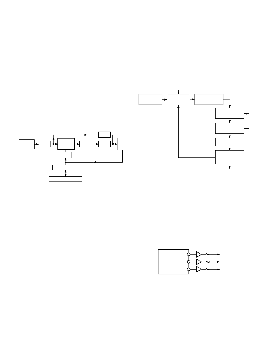
AD6620
38
REV. A
APPLICATIONS
EVALUATION BOARD
An evaluation board is available for the AD6620. This evalua-
tion board comes complete with an AD6620 and interfaces to a
PC through the printer port. The evaluation board comes com-
plete with software to drive the evaluation board and to design
optimized filters for use with the AD6620. The evaluation board
includes a high speed data interface that mates directly with
evaluation boards for high performance converters such as the
AD6600 and AD6640, allowing digital receivers to be bread-
boarded with only an external RF/IF converter and an interface
to the DSP.
The control software allows access to all of the internal registers
to provide complete programming of the device in a lab setting.
The software can process high speed data as well as digitally
filtered data from the AD6620 allowing analysis of both pre and
post filter channel characteristics. The controlling software can
also be used to verify the filter performance by sweeping the NCO,
greatly simplifying verification of any given filter design.
AD6620
HI SPEED
DATA
HEADER
LATCH
FIFO
PC PRINTER PORT
LATCH
LATCH
LATCH
TRANSCEIVER
Figure 47. Evaluation Board Block Diagram
As shown in the block diagram below, the high speed data into
the evaluation board is sent to both the AD6620 and the by-pass
latches. On the output of the AD6620, data is available in either
serial or parallel mode. In serial mode, data may be sent directly
to a DSP for system bread-boarding. In parallel mode, the data
may be sent to the on-board FIFO for spectral analysis by the
included software. For additional information, refer to the evalua-
tion board manual.
FILTER DESIGN
The AD6620 implements a pair of cascaded CIC filters with a
sum of products FIR filter. The frequency characteristics of the
CIC filters have already been documented. Additional reading
on this class of filters can be found in "An Economical Class of
Digital Filters for Decimation and Interpolation," by Eugene B.
Hogenauer, IEEE Transactions on Acoustics, Speech, and Signal
Processing, Volume ASSP-29, Number 2, April 1981.
The characteristics of the FIR filter are fully programmable.
The coefficients of this filter may be generated in any number
of ways, using standard procedures such as Parks-McClellan.
Available software from Analog Devices that assists in the design
of filters for this product. This software allows comparison
between different distributions of decimation. The software
works independently of the evaluation board, but easily allows
transfer of design data directly to the evaluation board for
immediate verification of the designed filter.
The normal procedure for designing a filter for the chip is as
shown in the flow chart. First, the desired characteristics must
be determined based on the receive channel requirements. The
decimation rates for the CIC filters must then be selected such
that their performance is near that of the desired channel require-
ments. Finally, an algorithm such as the Parks-McClellan or
Remez exchange is used to compute the final spectral require-
ments, including droop correction for passband loss of the CIC
filters. If the designed filter meets the requirements, then the
filter is acceptable. If not, another combination of CIC filter
decimation must be examined. Tables III and IV greatly simplify
distribution and selection of CIC requirements. The filter
software available from Analog Devices helps to automate
this procedure.
SELECT FILTER
REJECTION
REQUIREMENTS
DOES CIC2 FILTER
PROTECT ENOUGH
BANDWIDTH?
SELECT
DECIMATION
RATE FOR CIC5
DESIGN RCF WITH
REMEZ EXCHANGE
NO
YES
SELECT
DECIMATION
RATE FOR CIC2
DOES CIC5 FILTER
PROTECT ENOUGH
BANDWIDTH?
DOES COMPOSITE
FILTER PROVIDE
THE DESIRED
RESULTS?
YES
NO
YES
NO
Figure 48. Diagram of Filter Design Software
SERIAL BUFFERING
The AD6620 serial outputs are designed to operate at very high
speed. As such, care must be taken when driving the serial output
lines. These high speed lines must be treated as transmission
lines. Critical lines include the SCLK, SDFS, SDFE, SDI and
SDO. It is recommended that these lines be series source termi-
nated with the characteristic impedance of the driven line. If the
lines are longer than a few inches, digital line buffers should be
used as shown below. Buffering in this manner will prevent
reflections on the serial lines from disrupting operation of the
AD6620. A good reference on transmission lines is found in the
"MECL System Design Handbook" by Motorola Inc., Stock
code HB205R1/D.
AD6620
SCLK
SDO
SDFS
SCLK
SDO
SDFS
Figure 49. Serial Line Buffering and Series Source
Termination
DSP/SHARC INTERFACING
With little effort, the AD6620 will interface to nearly all indus-
try standard DSPs, as shown in the figure below. The figures
below show operation in TDM applications as well as in serial
slave mode.
In TDM mode the first AD6620 is configured to be the master.
This chip is the first to access the serial data bus. When the
master has data available in its output shifters, it generates an
SDFS telling the DSP that serial data will follow. At this point,
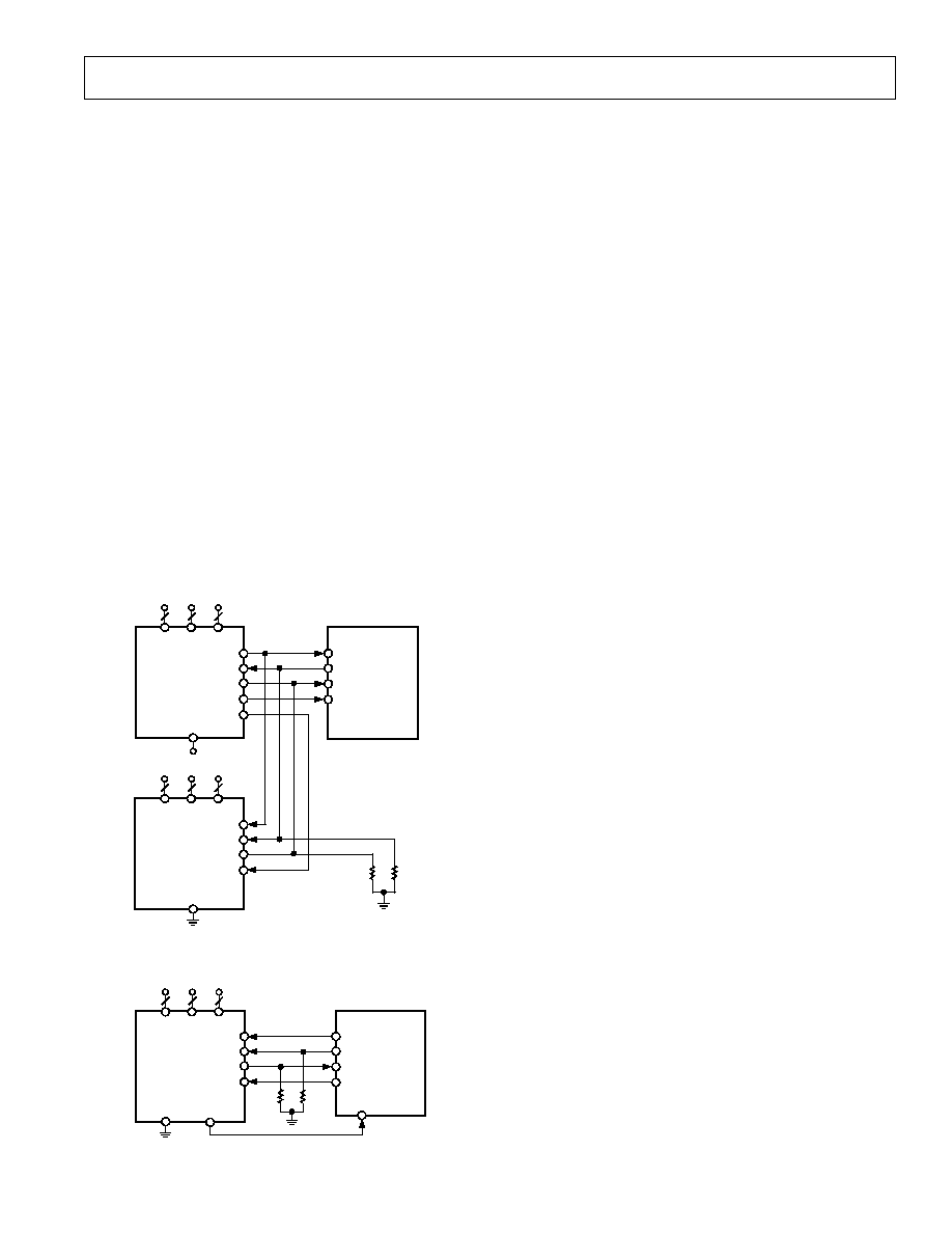
AD6620
39
REV. A
the SDO of the master AD6620 takes control of the SDO line
and begins shifting data out of the device. When all data has
been shifted, the master raises the SDFE on the last shifted.
This signals the next chip (slave) that on the next cycle of the
clock it should take control of the SDO line and begin shifting
data to the DSP. When the second AD6620 completes its shift,
it raises its SDFE to signal the next chip in the chain, if present.
If additional devices are connected to the chain, this would be
used to indicate they should take control on the next clock cycle.
This application does not have a third device and therefore, the
frame would end.
Normally in an application with a single AD6620, the AD6620
would be configured as the serial bus master. However, there
are applications where the DSP or other device may be the serial
bus master. In this case, the diagram below illustrates how to
configure the AD6620 so that it may be used in this mode. In
order to use this in a meaningful application, the DSP must
know when the AD6620 has new data available on its output. If
the DSP polls the AD6620 too early, either old data will be present
or the data could be in an indeterminate state. To prevent this,
the AD6620 has an output pin DV
OUT
that signals the DSP
when new data is available. This should be tied to an interrupt
line of the DSP that is edge-sensitive, as the DV
OUT
line is only
valid for two or four high speed clock cycles depending on the
mode of the chip. The DSP may then invoke an interrupt service
routine to handle the data, see text below. In this application,
the DSP is responsible for generating the framing and clocking
signals to the AD6620 as shown in Figure 51.
SCLK
AD6620
DSP
+3.3V
SBM
SCLK
SDI
DT
SDO
DR
SDFS
RFS
SDFE
10k
SDIV
2
4
AD
WL
10k
SCLK
SBM
SDI
SDO
SDFS
SDFE
SDIV
2
4
AD
WL
AD6620
CASCADE
Figure 50. Dual AD6620s Using the Serial Bus in a TDM
Application
SCLK
AD6620
DSP
SCLK
SDI
DT
SDO
DR
SDFS
RFS
SDFE
10k
SDIV
2
4
AD
WL
10k
SBM
DV
OUT
IRQ
Figure 51. AD6620 Configured as a Serial Slave
Software for Single Channel Real Operation
When interfacing Analog Device's SHARC DSP, the following
code fragments can be used to configure the SHARC. The first
example shows how to configure the registers for use with a single
channel application. The first segment of code defines the memory
for use with the multichannel serial port data. The second segment
of code sets up the serial port for receiving data only. It could
have just as easily been set up for bidirectional data by properly
setting the MTCSI register. The final two code segments are used
when a serial port interrupt occurs. When the SHARC detects
completion of the serial port frame, an interrupt is generated
and the final code segment is executed. The comments in that
section show where user code should be inserted. The SHARC
takes care of moving the serial port buffers data directly to data
memory as shown.
/
* ----------------------------------------------------------*/
/
* multi-channel register setup */
.SEGMENT/DM dm_data;
.VAR fm_demod_data[2];
/
* Array for receiving 1 real and imag
sample
*/
.VAR fm_demod_tcb[8] = 0, 0, 0, 0, fm_demod_data+7, 2, 1,
fm_demod_data;
/
* Transfer Control Block for reception of fm data */
/
* ----------------------------------------------------------*/
/
* ----------------------------------------------------------*/
/
* Subroutine to setup sport1 for use with the AD6620 */
setup_sport1:
r0 = 0;
/
* multi-channel enable setup */
dm(MTCS1) = r0;
/
* do not transmit on any channels */
r0 = 0;
/
* Compand Setup */
dm(MTCCS1) = r0;
/
* no companding on transmit */
dm(MRCCS1) = r0;
/
* no companding on receive */
r0 = 0x00100000;
/
* Setup sport 1 transmit control register */
dm(STCTL1) = r0;
/
* mfd = 1 */
r0 = 0x038c20f2;
/
* Setup sport 1 receive control register */
dm(SRCTL1) = r0;
/
* slen = 15, sden & schen enabled */
/
* sign extend, external SCLK+RFS */
r0 = fm_demod_tcb + 7; /
* TCB address */
dm(CP1) = r0;
/
* Kickoff DMA chain */
rts (db);
/
* RETURN */
bit set imask SPR1I;
/
* enable sport1 receive interrupt */
nop;
/
* ----------------------------------------------------------*/
spr1_svc:
jump spr1_asserted;
RTI;
RTI;
RTI;
/
* ----------------------------------------------------------*/
/
* ----------------------------------------------------------*/
/
* Process received data here. Data samples located in fm_demod_data
and fm_demod_data+1
spr1_asserted:
push sts;
/
* Push the status stack */
/
* Use secondary set of DAGs and Register file */

AD6620
40
REV. A
bit set mode1 SRD1H | SRD2L | SRRFH | SRRFL;
nop;
/
* Insert code here to process I and Q data. The DSP serial port handler
has placed the samples in fm_demod_data and fm_demod_data+1
*/
pop sts;
/
* Pop the status stack */
rti (db);
/
* Switch back to primary set of DAGs and Register file */
bit clr mode1 SRD1H | SRD2L | SRRFH | SRRFL;
nop;
.ENDSEG;
/
*----------------------------------------------------------*/
Software for Diversity Channel Real Operation
The code for interfacing to Diversity Channel Real mode is very
similar to that of single channel. The only difference being the
number of channels allocated on the TDM chain. This process
can easily be extended for any number of TDM channels as
long as there is sufficient time in the frame to completely trans-
mit the data. This procedure works with the appended data as
well as serially cascaded devices. The code below demonstrates
setup and operation in diversity channel mode.
/
*----------------------------------------------------------*/
.SEGMENT/DM dm_data;
/
* multi-channel register setup */
.VAR fm_demod_data[4];
/
* Array for receiving 2 real and imag
sample from each channel
*/
.VAR fm_demod_tcb[8] = 0, 0, 0, 0, 0, 4, 1, fm_demod_data;
/
* Transfer Control Block for reception of fm data */
/
* ----------------------------------------------------------*/
/
*----------------------------------------------------------*/
setup_sport1:
r0 = 0;
/
* multi-channel enable setup */
dm(MTCS1) = r0;
/
* do not transmit on any channels */
r0 = 0;
/
* Compand Setup */
dm(MTCCS1) = r0;
/
* no companding on transmit */
dm(MRCCS1) = r0;
/
* no companding on receive */
r0 = 0x00100000;
/
* Setup sport 1 transmit control register */
dm(STCTL1) = r0;
/
* mfd = 1 */
r0 = 0x038c00f2;
/
* Setup sport 1 receive control register */
dm(SRCTL1) = r0;
/
* slen = 15, sden & schen enabled */
/
* sign extend, external SCLK+RFS */
r0 = fm_demod_tcb + 7; /
* TCB address */
dm(fm_demod_tcb + 4) = r0;
/
* TCB point back to itself */
dm(CP1) = r0;
/
* Kickoff DMA chain */
rts (db)
/
* RETURN */
bit set imask SPR1I;
/
* enable sport1 receive interrupt */
bit set imask CB15I;
/
* Enable circular buffer 15 wrap
interrupt for buffers full
*/
/
*----------------------------------------------------------*/
/
*----------------------------------------------------------*/
spr1_svc:
jump spr1_asserted;
RTI;
RTI;
RTI;
/
*----------------------------------------------------------*/
/
*----------------------------------------------------------*/
spr1_asserted: /
* SPORT1 Receive interrupt - do the fm demod and
increment the counter
*/
push sts;
/
* Push the status stack */
/
* Use secondary set of DAGs and Register file */
bit set mode1 SRD1H | SRD1L | SRD2H | SRD2L | SRRFH |
SRRFL;
nop;
/
* Insert code here for processing I and Q data pairs. The DSP serial
port handler has placed the samples in fm_demod_data through
fm_demod_data+3
*/
pop sts;
/
* Pop the status stack */
rti (db);
/
* Switch back to primary set of DAGs and Register file */
bit clr mode1 SRD1H | SRD1L | SRD2H | SRD2L | SRRFH |
SRRFL;
nop;
.ENDSEG;
/
*----------------------------------------------------------*/
TYPICAL LATENCY EXPECTATIONS
In the AD6620 latency can be divided into three components.
For difficult filters, the largest component of latency is Algorith-
mic Latency. This type of latency is tied inseparably to the desired
filter response. For smaller or minimal filters, Fixed Latency begins
to dominate. This is the undesirable fixed delay associated with
the calculation of the output samples. Finally, Variable Latency,
is the smallest component. This is the delay that can be influenced
by the relative phase of internal decimated clocks with respect to
the SYNC_CIC.
Algorithmic Latency is a necessary component of any filtering
process be it analog or digital. Since frequency is a variation
with respect to time, it must take time to discriminate between
analog frequencies. Assuming the AD6620 is used to generate
linear phase, low-pass filters, the algorithmic latency is a direct
function of the number of RCF taps and the CIC decimation
ratios. In general, the largest part of the impulse response of
these filters is the center of the impulse response length, so that
the delay is represented by one-half the composite impulse
response length.
The impulse response length of the RCF is the number of taps
times the RCF input sample period. Therefore relative to the
input sample clock the impulse response length of the RCF is
given by;
N
M
M
f
TAPS
CIC
CIC
ADC
-
(
)
×
×
+
1
1
5
2
The impulse response length of the CIC5 is given by;
5
5
1
5
2
×
-
(
)
×
+
M
M
f
CIC
CIC
ADC
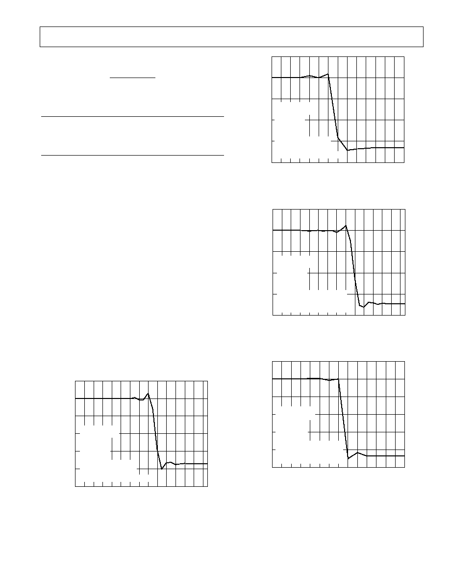
AD6620
41
REV. A
The impulse response length of the CIC2 is given by
2
1
2
×
-
(
)
M
f
CIC
ADC
The composite impulse response length of all three stages is
N
M
M
M
M
M
f
TAPS
CIC
CIC
CIC
CIC
CIC
ADC
×
×
+ ×
×
- ×
+
5
2
5
2
2
4
3
1
The Algorithmic Latency is
N
M
M
M
M
M
f
TAPS
CIC
CIC
CIC
CIC
CIC
ADC
×
×
+ ×
×
- ×
+
×
5
2
5
2
2
4
3
1
2
Fixed Latency is the delay due to each register between the input
and the output of the AD6620. The latency is the count of each
register multiplied by the period of the clock that drives it. The
fixed latency of the AD6620 can be approximated by the follow-
ing expression:
10
7
7
5
2
5
t
t
M
M
M
N
t
CLK
SAMP
CIC
CIC
RCF
TAPS
CLK
+
+
+
+
[
]
[
]
[
]
+
×
where:
t
CLK
is the high speed clock to the AD6620.
t
SAMP
is the data rate delivered to the AD6620.
Normally t
CLK
and t
SAMP
are the same unless a clock multiplier is
used such as with the AD6600's 2
× clock output.
Variable Latency is due to any differences between the asyn-
chronous edge of the SYNC pulses and the data rate. This
includes use of the internal synchronization options.
Based on the information on latency, the plots shown below
provide typical latency for a variety of different applications.
They were obtained by inserting a F
S
dc step into the Input Data
Port of the AD6620. These are I channel step responses for the
input transient. The latency is defined as the output period times
number of output samples until the output reached approxi-
mately 50% of the step value.
OUTPUT SAMPLES
0.20
0.40
1.00
1
21
3
FRACTION OF F
S
5
7
9
11 13
15 17
19
0.00
0.20
0.60
0.80
23
25
27 29
61.44MHz
SAMPLE RATE
M
CIC2
= 16
M
CIC5
= 8
M
RCF
= 8
N
TAPS
= 256
AT 19 OUTPUT SAMPLES,
THE LATENCY WOULD
BE 0.32ms
EXPECTED LATENCY = 0.303ms
Figure 52. AMPS Example
OUTPUT SAMPLES
0.20
0.40
1
11
2
FRACTION OF F
S
3
4
5
6
7
8
9
10
0.00
0.20
0.60
0.80
12
13
14
15
58.9824MHz
SAMPLE RATE
M
CIC2
= 2
M
CIC5
= 4
M
RCF
= 6
N
TAPS
= 48
AT 8 OUTPUT SAMPLES,
THE LATENCY WOULD
BE 6.51 s
EXPECTED LATENCY = 6.31 s
Figure 53. CDMA Example
OUTPUT SAMPLES
0.20
0.40
1
21
3
FRACTION OF F
S
5
7
9
11 13
15 17
19
0.00
0.20
0.60
0.80
23
25
27 29
64.512MHz
SAMPLE RATE
M
CIC2
= 2
M
CIC5
= 14
M
RCF
= 3
N
TAPS
= 84
AT 19 OUTPUT SAMPLES,
THE LATENCY WOULD
BE 24.7 s
EXPECTED LATENCY = 24.31 s
Figure 54. PHS Example
OUTPUT SAMPLES
0.20
0.40
1
11
2
FRACTION OF F
S
3
4
5
6
7
8
9
10
0.00
0.20
0.60
0.80
12
13
14
15
1.00
65.0MHz
SAMPLE RATE
M
CIC2
= 2
M
CIC5
= 6
M
RCF
= 20
N
TAPS
= 240
AT 9 OUTPUT SAMPLES,
THE LATENCY WOULD
BE 33.23 s
EXPECTED LATENCY = 31.2 s
Figure 55. WB-GSM Example
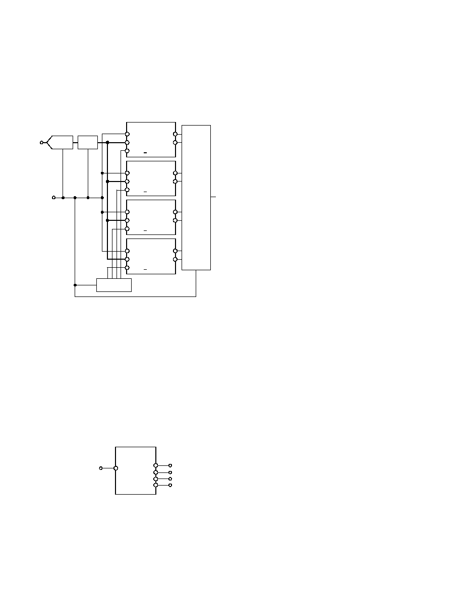
AD6620
42
REV. A
PARALLEL PROCESSING USING AD6620
If a single AD6620 does not have enough time to compute an
adequate filter, multiple AD6620s can be operated in parallel as
shown in Figure 56. In this example, the processing is distrib-
uted between four chips so that each chip can process more
taps. The outputs are then combined such that the desired data
rate is achieved.
CLK
D
IN
SYNC RCF
D
OUT
DV
OUT
AD6620 #1
AIN
ENCODE
CLOCK
CLK
D
IN
SYNC RCF
D
OUT
DV
OUT
AD6620 #2
CLK
D
IN
SYNC RCF
D
OUT
DV
OUT
AD6620 #4
CLK
D
IN
SYNC RCF
D
OUT
DV
OUT
AD6620 #3
LATCH
OUTPUT
SELECTOR
RCF TIMING
CONTROL
AD6640
Figure 56. Parallel Processing with the AD6620
In this application, one high speed ADC can feed parallel
AD6620s. Although not shown in this diagram, the SYNC_NCO
and SYNC_CICs are tied together and synchronized from an
external source with all chips run as SYNC_Slaves.
This architecture allows for each AD6620 to process four times
as many taps as would otherwise be possible. Consider the
example of an ADC clocked at 58.9824 MHz and a desired
output data rate of 4.9152 MHz. If a single AD6620 were used,
the decimation rate would be 12 (58.9824/4.9152) allowing for
only 12 taps in the FIR filter. Not nearly enough for a usable
digital filter. Now consider the case where each AD6620 only
provides an output for one in four samples. In this case, the
decimation rate per chip would be four times larger, 48 in this
example. With a decimation of 48, more taps for the filter can
be generated and produce a much better filter.
COUNTER
0 TO 47
CLOCK IN
COUNT = 0
COUNT = 11
COUNT = 23
COUNT = 35
Figure 57. RCF Timing Generator for Parallel Processing
Implementation of such a procedure is quite simple and basi-
cally shown in Figure 57. The filter design would proceed by
designing the filter to have the desired spectral characteristics
at its output rate. For our example here, each AD6620 would
have an output rate of 1.2288 MHz. The filter should be designed
such that the required rejection is attained directly at this rate.
This one filter is loaded into each chip. Upsampling is achieved
on the output by multiplexing between the different AD6620
outputs which are staggered, in this case by 90 degrees of the
output data rate. Therefore, since the decimation rate is 48
and four AD6620s are used, every 12 high speed clock cycles
a new AD6620 output should be selected. The most direct
method is to use these pulses to trigger the SYNC_RCF signals.
This staggering is required to properly phase the AD6620's inter-
nal computations. Once the chips have been synchronized in this
manner, they will begin producing DV
OUT
signals that can be
used to instruct the Output Selector which output is valid.
The RCF Timing Control is responsible for proper phasing of
the AD6620s in the system. The example shown here is for the
example of four devices in parallel. It can easily be expanded to
any number of devices with this methodology. Since the AD6620s
are decimating by 48, the complete cycle time is 48 system
clocks. Thus the timing control must run modulo 48. When the
count is 0, the first RCF should be reset with a pulse that is one
clock cycle wide. Likewise, when the count is 11, 23 and 35,
RCF2, RCF3 and RCF4 should be reset respectively. This will
properly phase the AD6620s to run 90 degrees out of phase. If
this example consisted of six AD6620s, then they should be
reset on count 0, 7, 15, 23, 31 and 39. Following this method,
any number of AD6620s can be paralleled for higher data rates.
Once the AD6620 RCFs are properly phased, the DV
OUT
signals
will then enable the output selector to know which outputs should
be connected at the correct point in time. In review, the DV
OUT
signal pulses high when the RCF data is being placed on the out-
puts. Since the devices are operated in Single Channel Real
mode, this signal will be high for two clock cycles while two
pieces of data are written to the output. The output pairs consist
of I followed by Q. As each chip's DV
OUT
cycles high, its data
should be connected to the output bus as shown below. This
effectively forms a MUX that sequentially cycles the output of
each of the AD6620s in the system to the output port. The only
remaining issue is retiming the data. Since each AD6620 clocks its
data out in two clock cycles, there will be 10 cycles where the
data is idle. During this period, the last Q out will remain valid
until the next chip in the sequence generates its DV
OUT
signal. This
normally should pose no problem, but if it does, the output data
could easily go to a FIFO and be retimed so that output data
streams at a regular rate.
In order to meet conventional logic requirements, OE for each
of the input latches should be active low. The DV
OUT
of the
AD6620 is active high, therefore, an inverter must be typically
inserted between the DV
OUT
lines and the OE of the latches as
shown in the updated Figure 58.
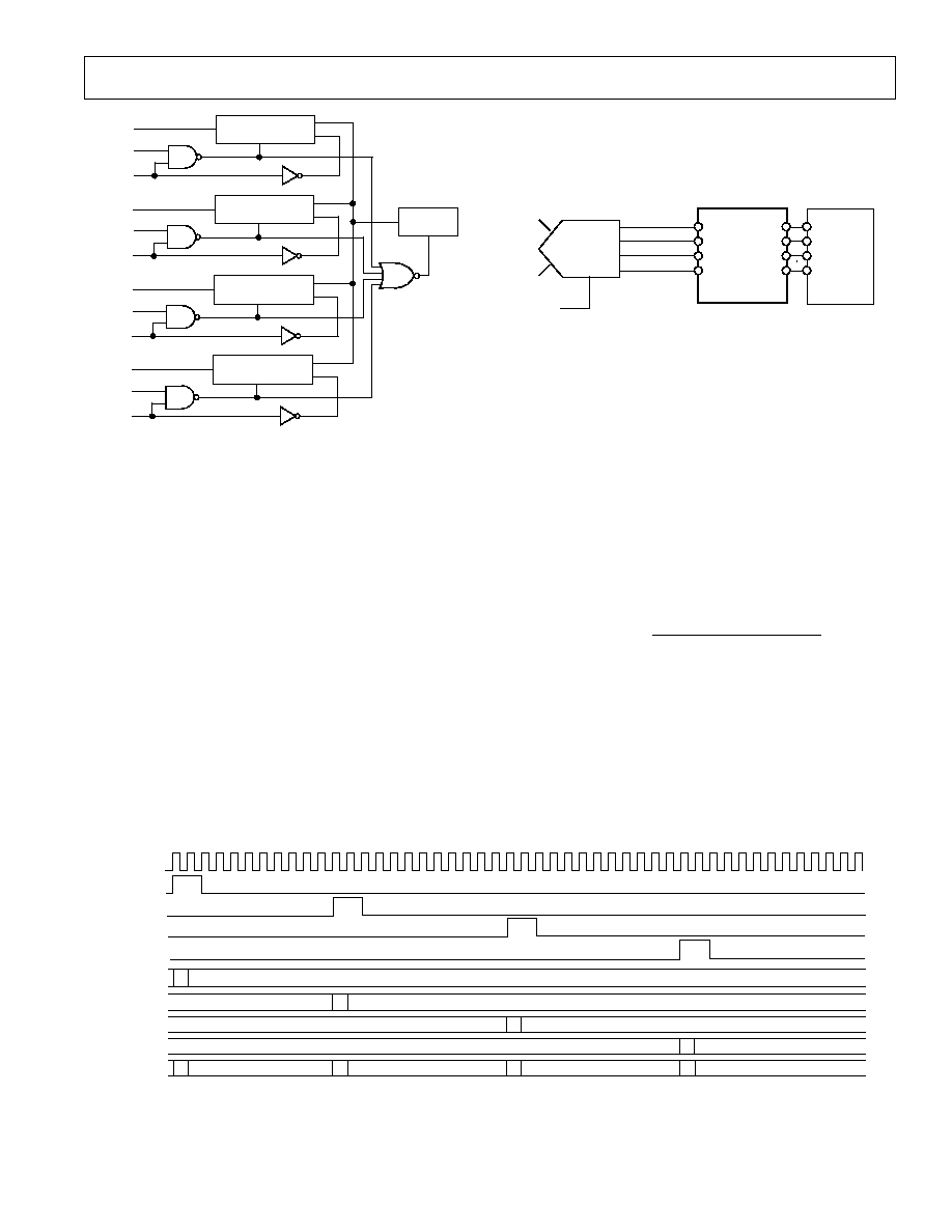
AD6620
43
REV. A
CLOCK
DV
OUT1
DV
OUT2
DV
OUT3
DV
OUT4
AD66201
AD66202
AD66203
AD66204
SELECTOR
OUTPUT
Q
I
Q
I
Q
I
Q
I
Q
I
Q
I
Q
I
Q
I
Figure 59. Timing for Parallel Processing
OE
INPUT LATCHING
D
OUT1
CLOCK
DV
OUT1
D
OUT2
CLOCK
DV
OUT2
D
OUT3
CLOCK
DV
OUT3
D
OUT4
CLOCK
DV
OUT4
OE
INPUT LATCHING
OE
INPUT LATCHING
OE
INPUT LATCHING
OUTPUT
LATCHING
Figure 58. Parallel Processing Output Selector
In the Output Selector above each of the DV
OUT
lines is ANDed
with main clock. This allows the data out of each of the AD6620s
to be properly latched into the input latches. The DV
OUT
line is
also responsible for placing the latched outputs on the internal
bus at the proper time. This data is then latched in the output
latch using the internal ORed clocking signals.
The timing for these events is shown in Figure 59. As shown,
the system clock is run at the specified rate. Then the RCF
timing control state machine is responsible for generating the
appropriate sync pulses. When each AD6620 completes its SOP
computation, it generates the DV
OUT
pulses shown below. Concur-
rently, each chip places its IQ data on the output pins of that
device. With this data, the output selector state machine com-
bines all of the data and places the data on the output bus.
Using the AD6620 in a Narrow Band System
A typical interconnection between the AD6600, AD6620 and a
General Purpose DSP is shown in Figure 65. This is an example
of an IF sampling narrow-band system and offers many techni-
cal and cost advantages over traditional solutions. In this example,
the AD6620 is in Diversity Channel Real Mode, with the AD6600
sampling a diversity antenna on its B channel. The AD6620
performs floating-point to fixed-point conversion, digital tuning,
digital filtering and decimation of the A/D output data.
MAIN
INPUT
DIVERSITY
INPUT
2 CLK
A/B OUT
3 RSSI BITS
11 DATA BITS
ENCODE
SCLK
SDI
SDO
SDFS
CLK
A/B
E[2...0]
IN[15...5]
AD6620
AD6600
SCLK
SDO
SDI
SDFS
DSP
Figure 60. Implementation of a Narrow Band Receiver
The 2
× CLK on the AD6600 is used as the processing CLK of
the AD6620. The use of this faster clock allows the RCF filter
to process up to twice as many taps per sample. The increased
number of taps available helps to improve the filter characteris-
tics. In some applications an even faster processing clock may be
necessary to allow for improved digital filter performance. In
this case the A/B pin of the AD6620 must be toggled when each
channel input is to be sampled.
For most narrow-band uses of the AD6600/AD6620 combina-
tion, a high oversampling ratio is desired. This spreads the
quantization noise of the A/D over a wider spectrum and allows
the digital filtering of the AD6620 to remove much of this noise.
This effectively increases the SNR of the AD6600. This process
of oversampling and digital filtering is called "process gain"
and its contribution to SNR can be calculated from the equa-
tion below.
PG
Sample Rate of Channel
Signal Bandwidth
=
10 log
_
_
_
_
The process of oversampling can also provide the benefit of
lowering the noise floor of the A/D. This can increase the effec-
tive dynamic range of a receiver if the sampling rate is chosen
such that the signal harmonics and/or intermodular distortion
(IMD) products fall out of the band of interest. In this case
these spurs could be filtered by the AD6620 and the quantiza-
tion noise would be the dominant dynamic range limitation of
the AD6600/AD6620 receiver solution.
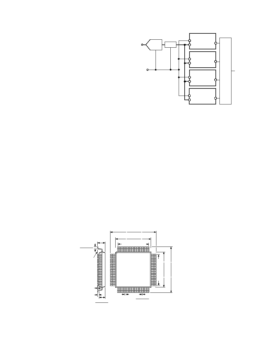
44
C0096706/01(A)
PRINTED IN U.S.A.
AD6620
REV. A
A DSP is then used to perform the demodulation of the digital
channel. This has the advantage of allowing for in-system con-
figuration options and can even allow for improved modulation
techniques to be applied in the future. This assumes that the
AD6600 and the circuitry on its front end are compatible with
the modulation standard to be used.
For more information on using the AD6600 and AD6620 in a
Single Carrier application, refer to Analog Devices' Application
note AN-502.
Using the AD6620 in a Wideband System
The AD6620 is fully capable of being utilized in a wide-band
architecture system where A/Ds such as the AD6640 or the
AD9042 usually run at higher sample rates than those typically
found in a narrow-band system. A correspondingly wider band
can then be digitized. The digitization of this wide bandwidth
allows many more channels to be digitized using the same A/D
and IF circuitry. The core configuration of such a system is
shown in Figure 61.
The AD6640 and the AD6620 are both designed to run as fast
as 67 MHz. In these applications the AD6620 will be used to
process only one channel and will process the data at the A/D
sample rate. Additional channels can be processed by taking the
AD6640 high speed data stream to additional AD6620s. Each
AD6620 can then be tuned to a different channel.
The AD6620 provides a great deal of selectivity by mixing down
a channel of interest as in the narrow-band case and filtering the
out-of-band noise and adjacent channels. Unlike the narrow-
band solutions it is much more difficult to place the spurious
content out of the band of interest because more of this band-
width is used due to the larger number of carrier channels. The
aliased spurs of one channel are likely to fold back on another
80-Lead Terminal Plastic Quad Flatpack (PQFP)
(S-80A)
SEATING
PLANE
0.134 (3.40)
MAX
0.041 (1.03)
0.029 (0.73)
0.004 (0.10)
MAX
0.120 (3.05)
0.100 (2.55)
0.010 (0.25)
MIN
0.015 (0.38)
0.009 (0.22)
0.690 (17.45)
0.667 (16.95)
0.555 (14.10)
0.547 (13.90)
0.555 (14.10)
0.547 (13.90)
0.690 (17.45)
0.667 (16.95)
1
20
21
41
40
60
61
80
0.486 (12.35) BSC
0.486 (12.35) BSC
TOP VIEW
(PINS DOWN)
0.026 (0.65)
BSC
OUTLINE DIMENSIONS
Dimensions shown in inches and (mm).
CLK
D
IN
AD6620 #1
SERIAL I/O
AIN
ENCODE
CLOCK
CLK
D
IN
AD6620 #2
SERIAL I/O
CLK
D
IN
AD6620 #3
SERIAL I/O
CLK
D
IN
AD6620 #4
SERIAL I/O
DSP
ARRAY
LATCH
AD6640
AD6644
Figure 61. Implementation of a Multicarrier Receiver
channel. This places a greater requirement on the Spurious Free
Dynamic Range (SFDR) of the A/D than in the narrow-band
case. The SFDR is then usually the limiting factor of the wide-
band system.
Provided that the A/D has sufficient SFDR for the air interface
requirements, the AD6620 can use process gain, as in the narrow-
band case, by filtering the out-of-band noise and adjacent channel
power. This increases the SNR of the digital data stream.
As in the Narrow-band System a DSP is then used to demodu-
late the digital data. The same advantages of flexibility exist in
the wide-band case as they did in the narrow-band case. Future
improvements in demodulation algorithms can be implemented
in the receiver, provided that the front end hardware is compat-
ible with the desired modulation standard.