 | ÐлекÑÑоннÑй компоненÑ: AD6624A | СкаÑаÑÑ:  PDF PDF  ZIP ZIP |
Äîêóìåíòàöèÿ è îïèñàíèÿ www.docs.chipfind.ru

REV. 0
Information furnished by Analog Devices is believed to be accurate and
reliable. However, no responsibility is assumed by Analog Devices for its
use, nor for any infringements of patents or other rights of third parties that
may result from its use. No license is granted by implication or otherwise
under any patent or patent rights of Analog Devices.
a
One Technology Way, P.O. Box 9106, Norwood, MA 02062-9106, U.S.A.
Tel: 781/329-4700
www.analog.com
Fax: 781/326-8703
© Analog Devices, Inc., 2002
AD6624A
The AD6624A is part of Analog Devices' SoftCell
®
multicarrier
transceiver chipset designed for compatibility with Analog
Devices' family of high sample rate IF sampling ADCs (AD6640/
AD6644 12- and 14-bit). The SoftCell receiver comprises a
digital receiver capable of digitizing an entire spectrum of
carriers and digitally selecting the carrier of interest for tuning
and channel selection. This architecture eliminates redundant
radios in wireless base station applications.
High dynamic range decimation filters offer a wide range of
decimation rates. The RAM-based architecture allows easy
reconfiguration for multimode applications.
The decimating filters remove unwanted signals and noise from
the channel of interest. When the channel of interest occupies less
bandwidth than the input signal, this rejection of out-of-band
noise is called "processing gain." By using large decimation
factors, this "processing gain" can improve the SNR of the
ADC by 30 dB or more. In addition, the programmable RAM
coefficient filter allows antialiasing, matched filtering, and
static equalization functions to be combined in a single, cost-
effective filter.
The AD6624A is compatible with standard ADC converters such
as the AD664x, AD9042, AD943x and the AD922x families of
data converters. The AD6624A is also compatible with the
AD6600 Diversity ADC, providing a cost and size reduction path.
Four-Channel, 100 MSPS Digital
Receive Signal Processor (RSP)
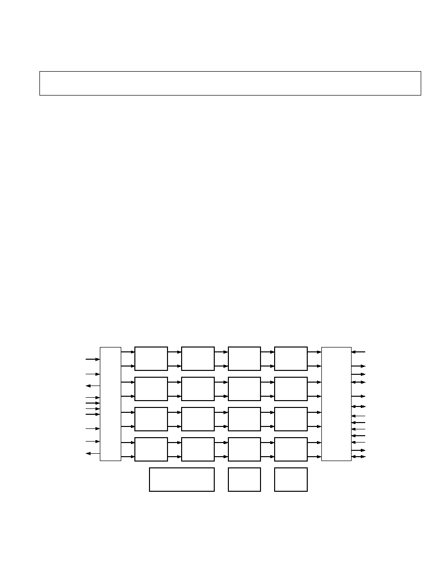
FUNCTIONAL BLOCK DIAGRAM
CH A
NCO
rCIC2
RESAMPLER
CIC5
RAM
COEFFICIENT
FILTER
16 BITS
18 BITS
20 BITS
24 BITS
INPUT
MATRIX
SERIAL
AND
MICROPORT
INA[13:0]
EXPA[2:0]
IENA
LIA-A
LIA-B
SYNCA
SYNCB
SYNCC
SYNCD
INB[13:0]
EXPB[2:0]
IENB
LIB-A
LIB-B
SDIN[3:0]
SDO[3:0]
DR[3:0]
SDFS[3:0]
SDFE[3:0]
SCLK[3:0]
MODE
DS(RD)
CS
RW(
WR)
DTACK(RDY)
A[2:0]
D[7:0]
CH B
NCO
rCIC2
RESAMPLER
CIC5
RAM
COEFFICIENT
FILTER
CH C
NCO
rCIC2
RESAMPLER
CIC5
RAM
COEFFICIENT
FILTER
CH D
NCO
rCIC2
RESAMPLER
CIC5
RAM
COEFFICIENT
FILTER
EXTERNAL SYNC
CIRCUITRY
JTAG
INTERFACE
BUILT-IN
SELF-TEST
FEATURES
100 MSPS Wideband Inputs (14 Linear Bits Plus 3 RSSI)
Dual High-Speed Data Input Ports
Four Independent Digital Receivers in Single Package
Digital Resampling for Noninteger Decimation Rates
Programmable Decimating FIR Filters
Programmable Attenuator Control for Clip Prevention
and External Gain Ranging via Level Indicator
Flexible Control for Multicarrier and Phased Array
3.3 V I/O, 2.5 V CMOS Core
User-Configurable Built-In Self-Test (BIST) Capability
JTAG Boundary Scan
APPLICATIONS
Multicarrier, Multimode Digital Receivers GSM, IS136,
EDGE, PHS, IS95
Micro and Pico Cell Systems
Wireless Local Loop
Smart Antenna Systems
Software Radios
In-Building Wireless Telephony
PRODUCT DESCRIPTION
The AD6624A is a four-channel (quad) digital receive signal
processor (RSP) with four cascaded signal-processing elements:
a frequency translator, two fixed-coefficient decimating filters,
and a programmable-coefficient decimating filter.
SoftCell is a registered trademark of Analog Devices, Inc.

REV. 0
AD6624A
2
FEATURES . . . . . . . . . . . . . . . . . . . . . . . . . . . . . . . . . . . . . . . . 1
GENERAL DESCRIPTION . . . . . . . . . . . . . . . . . . . . . . . . . . . 1
FUNCTIONAL BLOCK DIAGRAM . . . . . . . . . . . . . . . . . . . . 1
SPECIFICATIONS/CHARACTERISTICS . . . . . . . . . . . . . . . . 3
TIMING DIAGRAMS . . . . . . . . . . . . . . . . . . . . . . . . . . . . . . . . 6
ABSOLUTE MAXIMUM RATINGS . . . . . . . . . . . . . . . . . . . . 9
PIN FUNCTION DESCRIPTIONS . . . . . . . . . . . . . . . . . . . . 11
ARCHITECTURE . . . . . . . . . . . . . . . . . . . . . . . . . . . . . . . . . . 13
EXAMPLE FILTER RESPONSE . . . . . . . . . . . . . . . . . . . . . . 14
INPUT DATA PORTS . . . . . . . . . . . . . . . . . . . . . . . . . . . . . . . 14
Input Data Format . . . . . . . . . . . . . . . . . . . . . . . . . . . . . . . . . 14
Input Timing . . . . . . . . . . . . . . . . . . . . . . . . . . . . . . . . . . . . . 14
Input Enable Control . . . . . . . . . . . . . . . . . . . . . . . . . . . . . . . 14
Gain Switching . . . . . . . . . . . . . . . . . . . . . . . . . . . . . . . . . . . 15
Input Data Scaling . . . . . . . . . . . . . . . . . . . . . . . . . . . . . . . . . 16
Scaling with Fixed-Point ADCs . . . . . . . . . . . . . . . . . . . . . . . 16
Scaling with Floating-Point or Gain-Ranging ADCs . . . . . . . 16
NUMERICALLY CONTROLLED OSCILLATOR . . . . . . . . 17
Frequency Translation . . . . . . . . . . . . . . . . . . . . . . . . . . . . . . 17
NCO Frequency Hold-Off Register . . . . . . . . . . . . . . . . . . . . 17
Phase Offset . . . . . . . . . . . . . . . . . . . . . . . . . . . . . . . . . . . 17
NCO Control Register . . . . . . . . . . . . . . . . . . . . . . . . . . . . . . 17
Bypass . . . . . . . . . . . . . . . . . . . . . . . . . . . . . . . . . . . . . . . . . . 17
Phase Dither . . . . . . . . . . . . . . . . . . . . . . . . . . . . . . . . . . . . . 17
Amplitude Dither . . . . . . . . . . . . . . . . . . . . . . . . . . . . . . . . . . 17
Clear Phase Accumulator on HOP . . . . . . . . . . . . . . . . . . . . . 17
Input Enable Control . . . . . . . . . . . . . . . . . . . . . . . . . . . . . . . 17
Mode 00: Blank On IEN Low . . . . . . . . . . . . . . . . . . . . . . . . 17
Mode 01: Clock On IEN High . . . . . . . . . . . . . . . . . . . . . . . 18
Mode 10: Clock on IEN Transition to High . . . . . . . . . . . . . 18
Mode 11: Clock on IEN Transition to Low . . . . . . . . . . . . . . 18
WB Input Select . . . . . . . . . . . . . . . . . . . . . . . . . . . . . . . . . . . 18
Sync Select . . . . . . . . . . . . . . . . . . . . . . . . . . . . . . . . . . . . . . . 18
SECOND ORDER rCIC FILTER . . . . . . . . . . . . . . . . . . . . . . 18
rCIC2 Rejection . . . . . . . . . . . . . . . . . . . . . . . . . . . . . . . . . . . 19
Example Calculations . . . . . . . . . . . . . . . . . . . . . . . . . . . . . . 19
Decimation and Interpolation Registers . . . . . . . . . . . . . . . . . 19
rCIC2 Scale . . . . . . . . . . . . . . . . . . . . . . . . . . . . . . . . . . . . . . 19
FIFTH ORDER CASCADED INTEGRATOR COMB
FILTER . . . . . . . . . . . . . . . . . . . . . . . . . . . . . . . . . . . . . . . 20
CIC5 Rejection . . . . . . . . . . . . . . . . . . . . . . . . . . . . . . . . . 20
RAM COEFFICIENT FILTER . . . . . . . . . . . . . . . . . . . . . . . . 20
RCF Decimation Register . . . . . . . . . . . . . . . . . . . . . . . . . . . 21
RCF Decimation Phase . . . . . . . . . . . . . . . . . . . . . . . . . . . . . 21
RCF Filter Length . . . . . . . . . . . . . . . . . . . . . . . . . . . . . . . . . 21
RCF Output Scale Factor and Control Register . . . . . . . . . . 21
USER-CONFIGURABLE BUILT-IN SELF-TEST (BIST) . . 22
RAM BIST . . . . . . . . . . . . . . . . . . . . . . . . . . . . . . . . . . . . . . . . 22
CHANNEL BIST . . . . . . . . . . . . . . . . . . . . . . . . . . . . . . . . . . . 22
CHIP SYNCHRONIZATION . . . . . . . . . . . . . . . . . . . . . . . . . 22
Start . . . . . . . . . . . . . . . . . . . . . . . . . . . . . . . . . . . . . . . . . . . . 23
Hop . . . . . . . . . . . . . . . . . . . . . . . . . . . . . . . . . . . . . . . . . . . . 23
SERIAL OUTPUT DATA PORT . . . . . . . . . . . . . . . . . . . . . . 24
Serial Output Data Format . . . . . . . . . . . . . . . . . . . . . . . . . . 24
Compact Serial Data Format . . . . . . . . . . . . . . . . . . . . . . . . . 24
Serial Data Frame (Serial Bus Master) . . . . . . . . . . . . . . . . . . 24
Serial Data Frame (Serial Cascade) . . . . . . . . . . . . . . . . . . . . 25
Configuring the Serial Ports . . . . . . . . . . . . . . . . . . . . . . . . . . 25
Serial Port Data Rate . . . . . . . . . . . . . . . . . . . . . . . . . . . . . . . 25
Serial Port to DSP Interconnection . . . . . . . . . . . . . . . . . . . . 25
Serial Slave Operation . . . . . . . . . . . . . . . . . . . . . . . . . . . . . . 26
Serial Ports Cascaded . . . . . . . . . . . . . . . . . . . . . . . . . . . . . . . 26
Serial Output Frame Timing (Master and Slave) . . . . . . . . . . 26
Serial Port Timing Specifications . . . . . . . . . . . . . . . . . . . . . . 28
SBM0 . . . . . . . . . . . . . . . . . . . . . . . . . . . . . . . . . . . . . . . . . . 29
SCLK . . . . . . . . . . . . . . . . . . . . . . . . . . . . . . . . . . . . . . . . . . 29
SDIN . . . . . . . . . . . . . . . . . . . . . . . . . . . . . . . . . . . . . . . . . . . 29
SDO . . . . . . . . . . . . . . . . . . . . . . . . . . . . . . . . . . . . . . . . . . . . 29
SDFS . . . . . . . . . . . . . . . . . . . . . . . . . . . . . . . . . . . . . . . . . . . 29
SDFE . . . . . . . . . . . . . . . . . . . . . . . . . . . . . . . . . . . . . . . . . . . 29
Serial Word Length . . . . . . . . . . . . . . . . . . . . . . . . . . . . . . . . 29
SDFS Mode . . . . . . . . . . . . . . . . . . . . . . . . . . . . . . . . . . . . . . 29
Mapping RCF Data to the BIST Registers . . . . . . . . . . . . . . 30
0x000x7F: Coefficient Memory (CMEM) . . . . . . . . . . . . . . 30
0x80: Channel Sleep Register . . . . . . . . . . . . . . . . . . . . . . . . 30
0x81: Soft_SYNC Register . . . . . . . . . . . . . . . . . . . . . . . . . . 30
0x82: Pin_SYNC Register . . . . . . . . . . . . . . . . . . . . . . . . . . . 30
0x83: Start Hold-Off Counter . . . . . . . . . . . . . . . . . . . . . . . . 30
0x84: NCO Frequency Hold-Off Counter . . . . . . . . . . . . . . 30
0x85: NCO Frequency Register 0 . . . . . . . . . . . . . . . . . . . . . 30
0x86: NCO Frequency Register 1 . . . . . . . . . . . . . . . . . . . . . 30
0x87: NCO Phase Offset Register . . . . . . . . . . . . . . . . . . . . . 30
0x88: NCO Control Register . . . . . . . . . . . . . . . . . . . . . . . . . 30
0x90: rCIC2 Decimation 1 (M
rCIC2
1) . . . . . . . . . . . . . . . . 31
0x91: rCIC2 Interpolation 1 (L
rCIC2
1) . . . . . . . . . . . . . . . 31
0x92: rCIC2 Scale . . . . . . . . . . . . . . . . . . . . . . . . . . . . . . . . . 31
0x93: . . . . . . . . . . . . . . . . . . . . . . . . . . . . . . . . . . . . . . . . . . . 31
0x94: CIC5 Decimation 1 (M
CIC5
1) . . . . . . . . . . . . . . . . . 31
0x95: CIC5 Scale . . . . . . . . . . . . . . . . . . . . . . . . . . . . . . . . . 31
0x96: . . . . . . . . . . . . . . . . . . . . . . . . . . . . . . . . . . . . . . . . . . . 31
0xA0: RCF Decimation 1 (M
RCF
1) . . . . . . . . . . . . . . . . . . 31
0xA1: RCF Decimation Phase (P
RCF
) . . . . . . . . . . . . . . . . . . 31
0xA2: RCF Number of Taps Minus One (N
RCF
-1) . . . . . . . . 31
0xA3: RCF Coefficient Offset (CO
RCF
) . . . . . . . . . . . . . . . . . 31
0xA4: RCF Control Register . . . . . . . . . . . . . . . . . . . . . . . . . 31
0xA5: BIST Register for I . . . . . . . . . . . . . . . . . . . . . . . . . . . 32
0xA6: BIST Register for Q . . . . . . . . . . . . . . . . . . . . . . . . . . 32
0xA7: BIST Control Register . . . . . . . . . . . . . . . . . . . . . . . . 32
0xA8: RAM BIST Control Register . . . . . . . . . . . . . . . . . . . 32
0xA9: Serial Port Control Register . . . . . . . . . . . . . . . . . . . . 32
MICROPORT CONTROL . . . . . . . . . . . . . . . . . . . . . . . . . . . 33
External Memory Map . . . . . . . . . . . . . . . . . . . . . . . . . . . . . . 33
Access Control Register (ACR) . . . . . . . . . . . . . . . . . . . . . . . 33
External Memory Map . . . . . . . . . . . . . . . . . . . . . . . . . . . . 34
Channel Address Register (CAR) . . . . . . . . . . . . . . . . . . . . . . 34
SOFT_SYNC Control Register . . . . . . . . . . . . . . . . . . . . . . . 34
PIN_SYNC Control Register . . . . . . . . . . . . . . . . . . . . . . . . . 34
SLEEP Control Register . . . . . . . . . . . . . . . . . . . . . . . . . . . . 34
Data Address Registers . . . . . . . . . . . . . . . . . . . . . . . . . . . . . 35
Write Sequencing . . . . . . . . . . . . . . . . . . . . . . . . . . . . . . . . . . 35
Read Sequencing . . . . . . . . . . . . . . . . . . . . . . . . . . . . . . . . . . 35
Read/Write Chaining . . . . . . . . . . . . . . . . . . . . . . . . . . . . . . . 35
Intel Nonmultiplexed Mode (INM) . . . . . . . . . . . . . . . . . . . . 35
Motorola Nonmultiplexed Mode (MNM) . . . . . . . . . . . . . . . 35
Input Port Control Registers . . . . . . . . . . . . . . . . . . . . . . . . . 35
SERIAL PORT CONTROL . . . . . . . . . . . . . . . . . . . . . . . . . . . 36
JTAG BOUNDARY SCAN . . . . . . . . . . . . . . . . . . . . . . . . . . . 36
INTERNAL WRITE ACCESS . . . . . . . . . . . . . . . . . . . . . . . . . 37
Write Pseudocode . . . . . . . . . . . . . . . . . . . . . . . . . . . . . . . . . 37
INTERNAL READ ACCESS . . . . . . . . . . . . . . . . . . . . . . . . . . 38
Read Pseudocode . . . . . . . . . . . . . . . . . . . . . . . . . . . . . . . . . . 38
OUTLINE DIMENSIONS . . . . . . . . . . . . . . . . . . . . . . . . . . . . 39
TABLE OF CONTENTS

REV. 0
AD6624A
3
SPECIFICATIONS
(VDD = 2.5 V 5%, VDDIO = 3.3 V 10%. All specifications T
A
= T
MIN
to T
MAX
, unless otherwise noted.)
ELECTRICAL CHARACTERISTICS
Test
AD6624AS
Parameter (Conditions)
Temp
Level
Min
Typ
Max
Unit
LOGIC INPUTS
(5 V TOLERANT)
Logic Compatibility
Full
3.3 V CMOS
Logic "1" Voltage
Full
IV
2.0
5.0
V
Logic "0" Voltage
Full
IV
0.3
+0.8
V
Logic "1" Current
Full
IV
1
10
µA
Logic "0" Current
Full
IV
1
10
µA
Input Capacitance
25
°C
V
4
pF
LOGIC OUTPUTS
Logic Compatibility
Full
3.3 V CMOS/TTL
Logic "1" Voltage (I
OH
= 0.25 mA)
Full
IV
2.4
VDD 0.2
V
Logic "0" Voltage (I
OL
= 0.25 mA)
Full
IV
0.2
0.4
V
IDD SUPPLY CURRENT
CLK = 100 MHz, (VDD = 2.75 V, VDDIO = 3.6 V)
Full
IV
I
VDD
545
mA
I
VDDIO
60
mA
CLK = GSM Example (65 MSPS, VDD = 2.5 V,
VDDIO = 3.3 V, Dec = 2/10/6 120 Taps 4 Channels)
25
°C
V
I
VDD
250
mA
I
VDDIO
24
mA
POWER DISSIPATION
CLK = 80 MHz TD-SCDMA
Full
IV
1.1
W
CLK = 65 MHz
GSM/EDGE Example
V
700
mW
Sleep Mode
Full
IV
287
µW
Specifications subject to change without notice.
RECOMMENDED OPERATING CONDITIONS
Test
AD6624AS
Parameter
Level
Min
Typ
Max
Unit
VDD
IV
2.375
2.5
2.675
V
VDDIO
IV
3.0
3.3
3.6
V
T
AMBIENT
IV
40
+25
+70
°C

REV. 0
4
AD6624A
GENERAL TIMING CHARACTERISTICS
1, 2
Test
AD6624AS
Parameter (Conditions)
Temp
Level
Min
Typ
Max
Unit
CLK Timing Requirements:
t
CLK
CLK Period
Full
I
10
ns
t
CLKL
CLK Width Low
Full
IV
4.5
0.5
× t
CLK
ns
t
CLKH
CLK Width High
Full
IV
4.5
0.5
× t
CLK
ns
RESET Timing Requirement:
t
RESL
RESET Width Low
Full
I
30.0
ns
Input Wideband Data Timing Requirements:
t
SI
Input to
CLK Setup Time
Full
IV
0.8
ns
t
HI
Input to
CLK Hold Time
Full
IV
2.0
ns
Level Indicator Output Switching Characteristic:
t
DLI
CLK to LI (AA, B; BA, B) Output Delay Time
Full
IV
3.8
12.6
ns
SYNC Timing Requirements:
t
SS
SYNC (A, B, C, D) to
CLK Setup Time
Full
IV
1.0
ns
t
HS
SYNC (A, B, C, D) to
CLK Hold Time
Full
IV
2.0
ns
Serial Port Timing Requirements (SBM = 1):
Switching Characteristics:
3
t
DSCLK1
CLK to SCLK Delay (Divide by 1)
Full
IV
3.9
13.4
ns
t
DSCLKH
CLK to SCLK Delay (For Any Other Divisor)
Full
IV
4.4
14.0
ns
t
DSCLKL
CLK to SCLK Delay (Divide by 2 or Even #)
Full
IV
3.25
6.7
ns
t
DSCLKLL
CLK to SCLK Delay (Divide by 3 or Odd #)
Full
IV
3.8
6.9
ns
t
DSDFS
SCLK to SDFS Delay
Full
IV
0.2
5.3
ns
t
DSDFE
SCLK to SDFE Delay
Full
IV
0.4
+4.7
ns
t
DSDO
SCLK to SDO Delay
Full
IV
1.0
+4.0
ns
t
DSDR
SCLK to DR Delay
Full
IV
0.3
+4.6
ns
t
DDR
CLK to DR Delay
Full
IV
5.4
17.6
ns
Input Characteristics:
t
SSI
SDI to
SCLK Setup Time
Full
IV
2.4
ns
t
HSI
SDI to
SCLK Hold Time
Full
IV
3.0
ns
Serial Port Timing Requirements (SBM = 0):
Switching Characteristics:
3
t
SCLK
SCLK Period
Full
IV
16
ns
t
SCLKL
SCLK Low Time (When SDIV = 1, Divide by 1)
Full
IV
5.0
ns
t
SCLKH
SCLK High Time (When SDIV = 1, Divide by 1)
Full
IV
5.0
ns
t
DSDFE
SCLK to SDFE Delay
Full
IV
3.8
15.4
ns
t
DSDO
SCLK to SDO Delay
Full
IV
3.7
15.2
ns
t
DSDR
SCLK to DR Delay
Full
IV
3.9
15.9
ns
Input Characteristics:
t
SSF
SDFS to
SCLK Setup Time
Full
IV
1.9
ns
t
HSF
SDFS to
SCLK Hold Time
Full
IV
0.7
ns
t
SSI
SDI to
SCLK Setup Time
Full
IV
2.4
ns
t
HSI
SDI to
SCLK Hold Time
Full
IV
2.0
ns
NOTES
1
All Timing Specifications valid over VDD range of 2.375 V to 2.675 V and VDDIO range of 3.0 V to 3.6 V.
2
C
LOAD
= 40 pF on all outputs unless otherwise specified.
3
The timing parameters for SCLK, SDFS, SDFE, SDO, SDI, and DR apply to all four channels (0, 1, 2, and 3). The slave serial port's (SCLK) operating frequency is
limited to 62.5 MHz.
Specifications subject to change without notice.

REV. 0
AD6624A
5
MICROPROCESSOR PORT TIMING CHARACTERISTICS
1, 2
Test
AD6624AS
Parameter (Conditions)
Temp
Level
Min
Typ
Max
Unit
MICROPROCESSOR PORT, MODE INM (MODE = 0)
MODE INM Write Timing:
t
SC
Control
3
to
CLK Setup Time
Full
IV
5.5
ns
t
HC
Control
3
to
CLK Hold Time
Full
IV
1.0
ns
t
HWR
WR(RW) to RDY(DTACK) Hold Time
Full
IV
8.0
ns
t
SAM
Address/Data to
WR(RW) Setup Time
Full
IV
0.5
ns
t
HAM
Address/Data to RDY(
DTACK) Hold Time
Full
IV
7.0
ns
t
DRDY
WR(RW) to RDY(DTACK) Delay
Full
IV
4.0
ns
t
ACC
WR(RW) to RDY(DTACK) High Delay
Full
IV
4
× t
CLK
5
× t
CLK
9
× t
CLK
ns
MODE INM Read Timing:
t
SC
Control
3
to
CLK Setup Time
Full
IV
4.0
ns
t
HC
Control
3
to
CLK Hold Time
Full
IV
2.0
ns
t
SAM
Address to
RD(DS) Setup Time
Full
IV
0.0
ns
t
HAM
Address to Data Hold Time
Full
IV
7.0
ns
t
DRDY
RD(DS) to RDY(DTACK) Delay
Full
IV
4.0
ns
t
ACC
RD(DS) to RDY(DTACK) High Delay
Full
IV
8
× t
CLK
10
× t
CLK
13
× t
CLK
ns
MICROPROCESSOR PORT, MODE MNM (MODE = 1)
MODE MNM Write Timing:
t
SC
Control
3
to
CLK Setup Time
Full
IV
5.5
ns
t
HC
Control
3
to
CLK Hold Time
Full
IV
1.0
ns
t
HDS
DS(RD) to DTACK(RDY) Hold Time
Full
IV
8.0
ns
t
HRW
RW(
WR) to DTACK(RDY) Hold Time
Full
IV
8.0
ns
t
SAM
Address/Data to RW(
WR) Setup Time
Full
IV
0.5
ns
t
HAM
Address/Data to RW(
WR) Hold Time
Full
IV
7.0
ns
t
ACC
RW(
WR) to DTACK(RDY) Low Delay
Full
IV
4
× t
CLK
5
× t
CLK
9
× t
CLK
ns
MODE MNM Read Timing:
t
SC
Control
3
to
CLK Setup Time
Full
IV
4.0
ns
t
HC
Control
3
to
CLK Hold Time
Full
IV
2.0
ns
t
SAM
Address to
DS(RD) Setup Time
Full
IV
0.0
ns
t
HAM
Address to Data Hold Time
Full
IV
7.0
ns
t
ZD
Data Three-State Delay
Full
IV
7.0
ns
t
ACC
DS(RD) to DTACK(RDY) Low Delay
Full
IV
8
× t
CLK
10
× t
CLK
13
× t
CLK
ns
NOTES
1
All Timing Specifications valid over VDD range of 2.375 V to 2.675 V and VDDIO range of 3.0 V to 3.6 V.
2
C
LOAD
= 40 pF on all outputs unless otherwise specified.
3
Specification pertains to control signals: RW, (
WR), DS, (RD), CS.
Specifications subject to change without notice.

REV. 0
AD6624A
6
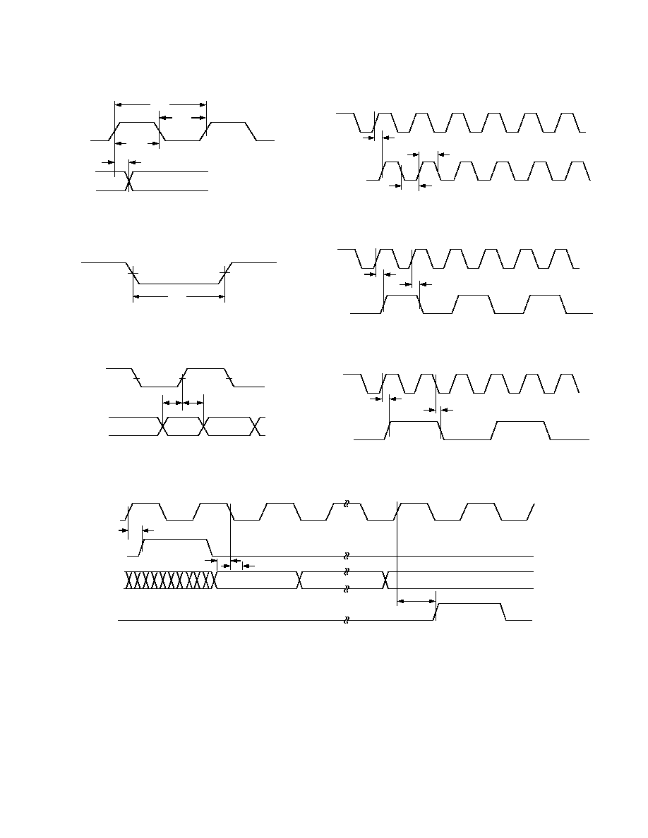
TIMING DIAGRAMS
CLK
LIA-A
LIA-B
LIB-A
LIB-B
t
DLI
t
CLK
t
CLKL
t
CLKH
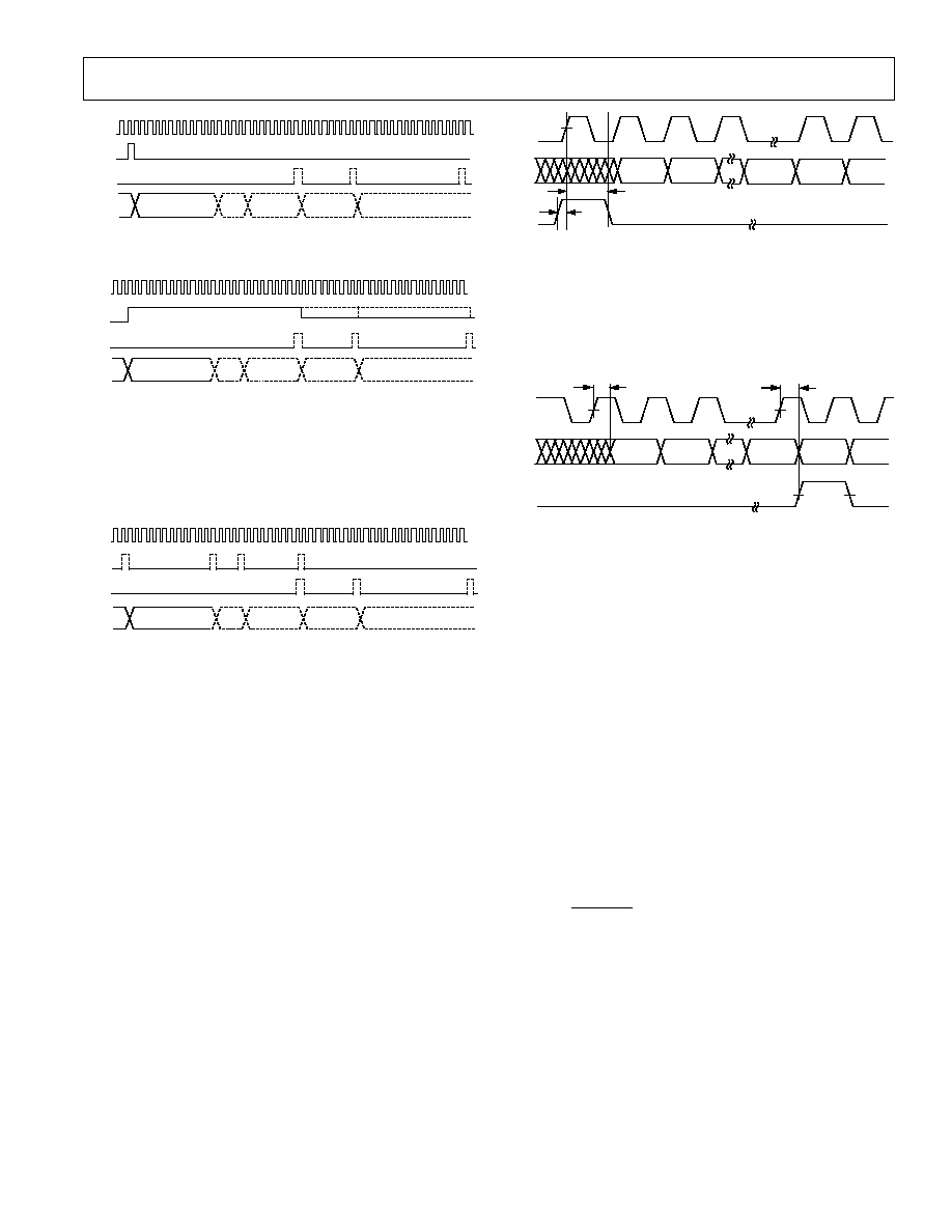
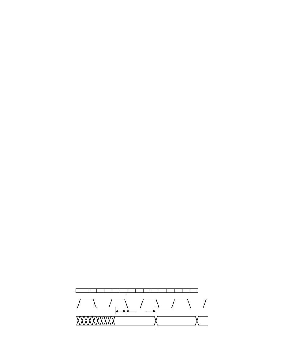
Figure 1. Level Indicator Output Switching
Characteristics
RESET
t
SSF
Figure 2.
RESET Timing Requirements
CLK
IN[13:0]
EXP[2:0]
DATA
t
SI
t
HI
Figure 3. Input Data Timing Requirements
CLK
SCLK
t
DSCLKH
t
SCLKH
t
SCLKL
Figure 4. SCLK Switching Characteristics (Divide by 1)
CLK
SCLK
t
DSCLKH
t
SCLKL
Figure 5. SCLK Switching Characteristic (Divide by 2 or
EVEN Integer)
CLK
SCLK
t
DSCLKH
t
DSCLKLL
Figure 6. SCLK Switching Characteristic (Divide by 3 or
ODD Integer)
SCLK
SDFS
SDI
SDFE
t
SSI
t
HSI
DATAn
t
DSDFE
t
DSDFS
Figure 7. Serial Port Switching Characteristics

REV. 0
AD6624A
7
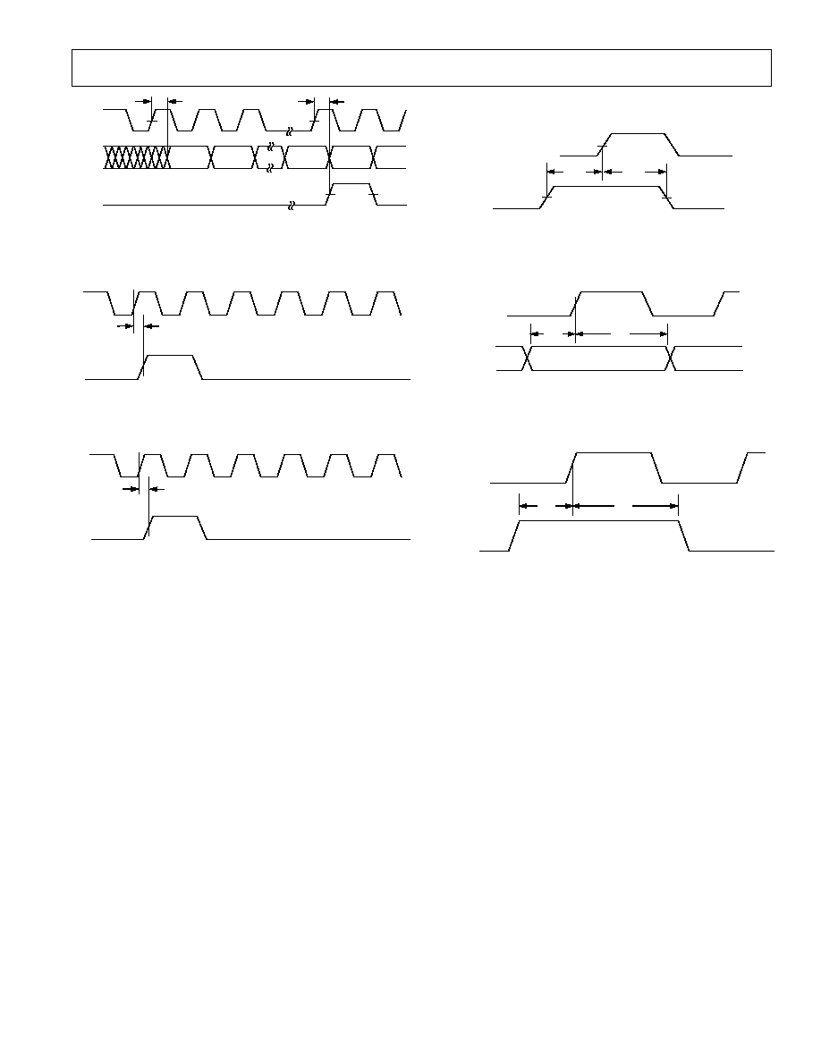
SCLK
SDO
SDFE
t
DSDO
t
DSDFE
Q
1
Q
0
I
14
I
15
Figure 8. SDO, SDFE Switching Characteristics
CLK
DR
t
DDR
Figure 9. CLK, DR Switching Characteristics
SCLK
DR
t
DSDR
Figure 10. SCLK, DR Switching Characteristics
SCLK
SDFS
t
SSF
t
HSF
Figure 11. SDFS Timing Requirements (SBM = 0)
CLK
IN[13:0]
EXP[2:0]
IEN
t
SI
t
HI
Figure 12. Input Timing for A and B Channels
CLK
SYNCA
SYNCB
SYNCC
SYNCD
t
SS
t
HS
Figure 13. SYNC Timing Inputs

REV. 0
AD6624A
8
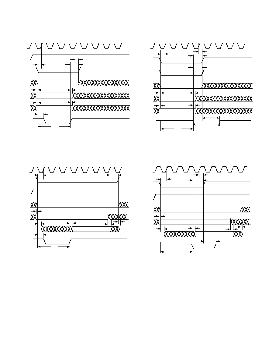
TIMING DIAGRAMS--INM MICROPORT MODE
CLK
RD(DS)
WR(RW)
CS
A[2:0]
D[7:0]
RDY
(
DTACK)
t
SC
t
HC
t
HWR
t
SAM
t
SAM
t
HAM
t
DRDY
VALID DATA
VALID ADDRESS
t
HAM
t
ACC
NOTES
1. t
ACC
ACCESS TIME DEPENDS ON THE ADDRESS ACCESSED. ACCESS TIME IS
MEASURED FROM FE OF
WR TO THE RE OF RDY.
2. t
ACC
REQUIRES A MAXIMUM 9 CLK PERIODS.
Figure 14. INM Microport Write Timing Requirements
CLK
RD (DS)
WR(RW)
A[2:0]
D[7:0]
RDY
(
DTACK)
t
SC
t
SAM
t
ZD
t
DRDY
VALID DATA
VALID ADDRESS
t
ACC
t
HC
CS
t
ZD
t
HAM
NOTES
1.
t
ACC
ACCESS TIME DEPENDS ON THE ADDRESS ACCESSED. ACCESS
TIME IS MEASURED FROM FE OF
WR TO THE RE OF RDY.
2.
t
ACC
REQUIRES A MAXIMUM OF 13 CLK PERIODS AND APPLIES TO
A[2:0] = 7, 6, 5, 3, 2, 1
t
DD
Figure 15. INM Microport Read Timing Requirements
TIMING DIAGRAMS--MNM MICROPORT MODE
CLK
DS(RD)
CS
A[2:0]
D[7:0]
DTACK
(RDY)
t
SC
t
HC
t
HRW
t
SAM
t
SAM
t
HAM
VALID DATA
VALID ADDRESS
t
HAM
t
ACC
NOTES
1.
t
ACC
ACCESS TIME DEPENDS ON THE ADDRESS ACCESSED. ACCESS TIME IS
MEASURED FROM FE OF
DS TO THE FE OF DTACK.
2.
t
ACC
REQUIRES A MAXIMUM 9 CLK PERIODS.
RW(
WR)
t
DDTACK
t
HDS
Figure 16. MNM Microport Write Timing Requirements
CLK
RD(DS)
WR(RW)
A[2:0]
D[7:0]
DTACK
(RDY)
t
SC
t
SAM
t
ZD
VALID DATA
VALID ADDRESS
t
ACC
t
HC
CS
t
ZD
t
HAM
t
DD
t
DDTACK
t
HDS
NOTES
1.
t
ACC
ACCESS TIME DEPENDS ON THE ADDRESS ACCESSED. ACCESS TIME IS
MEASURED FROM FE OF
DS TO THE FE OF DTACK.
2.
t
ACC
REQUIRES A MAXIMUM 13 CLK PERIODS.
Figure 17. MNM Microport Read Timing Requirements

REV. 0
AD6624A
9
ABSOLUTE MAXIMUM RATINGS
*
Supply Voltage . . . . . . . . . . . . . . . . . . . . . . . . . . . . . . . . 3.6 V
Input Voltage . . . . . . . . . . . . 0.3 V to +5.3 V (5 V Tolerant)
Output Voltage Swing . . . . . . . . . . 0.3 V to VDDIO + 0.3 V
Load Capacitance . . . . . . . . . . . . . . . . . . . . . . . . . . . . 200 pF
Junction Temperature Under Bias . . . . . . . . . . . . . . . . 125
°C
Storage Temperature Range . . . . . . . . . . . . 65
°C to +150°C
Lead Temperature (5 sec) . . . . . . . . . . . . . . . . . . . . . . . 280
°C
*Stresses greater than those listed above may cause permanent damage to the
device. These are stress ratings only; functional operation of the device at these or
any other conditions greater than those indicated in the operational sections of this
specification is not implied. Exposure to absolute maximum rating conditions for
extended periods may affect device reliability.
Thermal Characteristics
196-Lead Ball Grid Array:
JA
= 26.3
°C/W, No Airflow
JA
= 22
°C/W, 200 LFPM Airflow
Thermal measurements made in the horizontal position on
a 4-layer board.
EXPLANATION OF TEST LEVELS
I.
100% Production Tested.
II.
100% Production Tested at 25
°C, and Sample Tested at
Specified Temperatures.
III. Sample Tested Only.
IV. Parameter Guaranteed by Design and Analysis.
V.
Parameter is Typical Value Only.
VI. 100% Production Tested at 25
°C, and Sample Tested at
Temperature Extremes.
ORDERING GUIDE
Package
Model
Temperature Range
Package Description
Option
AD6624AABC
40
°C to +85°C (Ambient)
196-Lead BGA (Ball Grid Array)
BC-196
AD6624AS/PCB
Evaluation Board with AD6624A and Software
CAUTION
ESD (electrostatic discharge) sensitive device. Electrostatic charges as high as 4000 V readily
accumulate on the human body and test equipment and can discharge without detection.
Although the AD6624A features proprietary ESD protection circuitry, permanent damage may
occur on devices subjected to high-energy electrostatic discharges. Therefore, proper ESD
precautions are recommended to avoid performance degradation or loss of functionality.
WARNING!
ESD SENSITIVE DEVICE

REV. 0
AD6624A
10
PIN CONFIGURATION
(Top View)
1
2
3
4
5
6
7
8
9
10
11
12
13
14
NO
NC
INB5
INB6
INB12
EXPB1
EXPB0
SDIN3
SDFS3
DR2
SDFS2
NC
INB3
INB4
INB7
INB10
INB13
DR3
SDO3
SDFE2
SDO2
INB1
INB8
INB9
INB11
EXPB2
SDFE3
SCLK3
SDIN2
SCLK2
SDFE1
LIB-B
INB2
INB0
SDFS1
DR1
SDIN1
VDDIO
VDD
VDDIO
VDD
VDDIO
VDD
CLK
IENB
LIB-A
SDO1
VDD
GND
GND
GND
GND
VDDIO
EXPA1
EXPA0
EXPA2
SCLK1
DR0
SDIN0
VDDIO
GND
GND
GND
GND
VDD
INA12
INA13
INA10
SDFE0
SDO0
SCLK0
VDD
GND
GND
GND
GND
VDDIO
INA11
INA9
INA7
SDFS0
SDIV1
SDIV0
VDDIO
GND
GND
GND
GND
VDD
INA8
INA6
INA4
SDIV2
SMB0
SDIV3
VDD
VDDIO
VDD
VDDIO
VDD
VDDIO
INA5
INA2
INA0
CHIP ID1
CHIP ID3
CHIP ID0
INA1
INA3
TDI
TMS
CHIP ID2
IENA
SYNCD
SYNCA
D5
D2
DS(RD)
A0
MODE
TRST
TD0
LIA-A
SYNCC
D7
D4
D1
DTACK(RDY)
A2
CS
TCLK
NC
LIA-B
SYNCB
RESET
D6
D3
D0
RW(
WR)
A1
NC
A
B
C
D
E
F
G
H
J
K
L
M
N
P
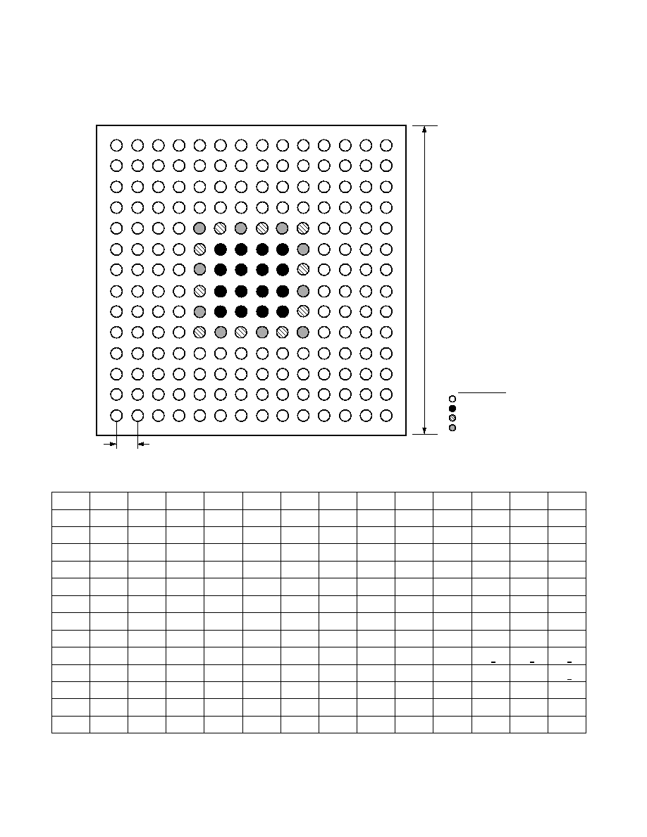
BALL LEGEND
I/O
GROUND
CORE POWER
RING POWER
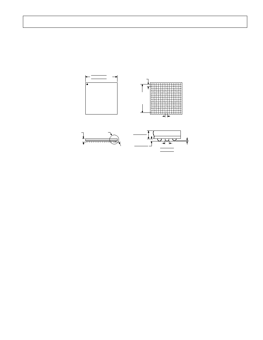
15mm SQ.
1.0mm.
A
B
C
D
E
F
G
H
J
K
L
M
N
P
1
2
3
4
5
6
7
8
9
10
11
12
13
14
TOP VIEW
NC = NO CONNECT

REV. 0
AD6624A
11
PIN FUNCTION DESCRIPTIONS 196-LEAD BGA
Pin No.
Type
Function
POWER SUPPLY
VDD
P
2.5 V Supply
VDDIO
P
3.3 V IO Supply
GND
G
Ground
INPUTS
INA[13:0]
1
I
A Input Data (Mantissa)
EXPA[2:0]
1
I
A Input Data (Exponent)
IENA
2
I
Input Enable--Input A
INB[13:0]
1
I
B Input Data (Mantissa)
EXPB[2:0]
1
I
B Input Data (Exponent)
IENB
2
I
Input Enable--Input B
RESET
I
Active Low Reset Pin
CLK
I
Input Clock
SYNCA
1
I
All Sync Pins Go to All Four Output Channels
SYNCB
1
I
All Sync Pins Go to All Four Output Channels
SYNCC
1
I
All Sync Pins Go to All Four Output Channels
SYNCD
1
I
All Sync Pins Go to All Four Output Channels
SDIN0
1
I
Serial Data Input--Channel 0
SDIN1
1
I
Serial Data Input--Channel 1
SDIN2
1
I
Serial Data Input--Channel 2
SDIN3
1
I
Serial Data Input--Channel 3
CS
1
I
Chip Select
CHIP_ID[3:0]
1
I
Chip ID Selector
CONTROL
SBM0
1
I
Serial Bus Master--Channel 0 only
SCLK0
1
I/O
Bidirectional Serial Clock--Channel 0
SCLK1
1
I/O
Bidirectional Serial Clock--Channel 1
SCLK2
1
I/O
Bidirectional Serial Clock--Channel 2
SCLK3
1
I/O
Bidirectional Serial Clock--Channel 3
SDIV[3:0]
1
I
Serial Clock Divisor--Channel 0
SDFS0
1
I/O
Bidirectional Serial Data Frame Sync--Channel 0
SDFS1
1
I/O
Bidirectional Serial Data Frame Sync--Channel 1
SDFS2
1
I/O
Bidirectional Serial Data Frame Sync--Channel 2
SDFS3
1
I/O
Bidirectional Serial Data Frame SyncvChannel 3
SDFE0
O
Serial Data Frame End--Channel 0
SDFE1
O
Serial Data Frame End--Channel 1
SDFE2
O
Serial Data Frame End--Channel 2
SDFE3
O
Serial Data Frame End--Channel 3
MICROPORT CONTROL
D[7:0]
I/O/T
Bidirectional Microport Data
A[2:0]
I
Microport Address Bus
DS (RD)
I
Active Low Data Strobe (Active Low Read)
DTACK (RDY)
2
O/T
Active Low Data Acknowledge (Microport Status Bit)
RW (
WR)
I
Read Write (Active Low Write)
MODE
I
Intel or Motorola Mode Select

REV. 0
AD6624A
12
PIN FUNCTION DESCRIPTIONS 196-LEAD BGA (continued)
Pin No.
Type
Function
OUTPUT
LIA-A
O
Level Indicator--Input A, Interleaved-Data A
LIA-B
O
Level Indicator--Input A, Interleaved-Data B
LIB-B
O
Level Indicator--Input B, Interleaved-Data B
LIB-A
O
Level Indicator--Input B, Interleaved-Data A
SDO0
1
O/T
Serial Data Output--Channel 0
SDO1
1
O/T
Serial Data Output--Channel 1
SDO2
1
O/T
Serial Data Output--Channel 2
SDO3
1
O/T
Serial Data Output--Channel 3
DR0
O
Output Data Ready Indicator--Channel 0
DR1
O
Output Data Ready Indicator--Channel 1
DR2
O
Output Data Ready Indicator--Channel 3
DR3
O
Output Data Ready Indicator--Channel 3
JTAG and BIST
TRST
2
I
Test Reset Pin
TCLK
1
I
Test Clock Input
TMS
2
I
Test Mode Input
TDO
O/T
Test Data Output
TDI
2
I
Test Data Input
NOTES
1
Pins with a pull-down resistor of nominal 70 k
.
2
Pins with a pull-up resistors of nominal 70 k
.

REV. 0
AD6624A
13
ARCHITECTURE
The AD6624A has four signal processing stages: a Frequency
Translator, second order Resampling Cascaded Integrator
Comb FIR filters (rCIC2), a fifth order Cascaded Integrator
Comb FIR filter (CIC5) and a RAM Coefficient FIR filter
(RCF). Multiple modes are supported for clocking data into and
out of the chip, and provide flexibility for interfacing to a wide
variety of digitizers. Programming and control is accomplished
via serial and microprocessor interfaces.
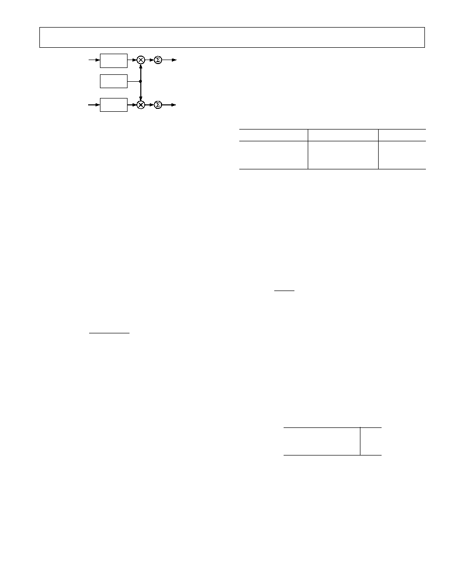
Frequency translation is accomplished with a 32-bit complex
Numerically Controlled Oscillator (NCO). Real data entering
this stage is separated into in-phase (I) and quadrature (Q)
components. This stage translates the input signal from a digital
intermediate frequency (IF) to digital baseband. Phase and
amplitude dither may be enabled on-chip to improve spurious
performance of the NCO. A phase-offset word is available to
create a known phase relationship between multiple AD6624s or
between channels.
Following frequency translation is a resampling, fixed-coefficient,
high-speed, second order, Resampling Cascade Integrator
Comb (rCIC2) filter that reduces the sample rate based on the
ratio between the decimation and interpolation registers.
The next stage is a fifth order Cascaded Integrator Comb (CIC5)
filter whose response is defined by the decimation rate. The
purpose of these filters is to reduce the data rate to the final
filter stage so it can calculate more taps per output.
The final stage is a sum-of-products FIR filter with program-
mable 20-bit coefficients, and decimation rates programmable
from 1 to 256 (132 in practice). The RAM Coefficient FIR
filter (RCF in the Functional Block Diagram) can handle a
maximum of 160 taps.
The overall filter response for the AD6624A is the composite of
all decimating and interpolating stages. Each successive filter
stage is capable of narrower transition bandwidths but requires
a greater number of CLK cycles to calculate the output. More
decimation in the first filter stage will minimize overall power
consumption. Data from the chip is interfaced to the DSP via a
high-speed synchronous serial port.
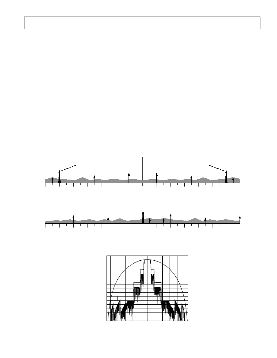
Figure 18a illustrates the basic function of the AD6624A: to
select and filter a single channel from a wide input spectrum.
The frequency translator "tunes" the desired carrier to baseband.
Figure 18b shows the combined filter response of the rCIC2,
CIC5, and RCF.
SIGNAL OF INTEREST
f
S
/2
WIDEBAND INPUT SPECTRUM (
f
SAMP
/ 2 TO +
f
SAMP
/ 2)
SIGNAL OF INTEREST "IMAGE"
3
f
S
/8
5
f
S
/ 16
f
S
/4
3
f
S
/ 16
f
S
/8
f
S
/16
DC
f
S
/16
f
S
/8
3
f
S
/16
f
S
/4
5
f
S
/16
3
f
S
/8
f
S
/2
WIDEBAND INPUT SPECTRUM (e.g., 30MHz FROM HIGH-SPEED ADC)
AFTER FREQUENCY TRANSLATION
NCO "TUNES" SIGNAL TO BASEBAND
FREQUENCY TRANSLATION (e.g., SINGLE 1MHz CHANNEL TUNED TO BASEBAND)
f
S
/2
3
f
S
/8
5
f
S
/ 16
f
S
/4
3
f
S
/ 16
f
S
/8
f
S
/16
DC
f
S
/16
f
S
/8
3
f
S
/16
f
S
/4
5
f
S
/16
3
f
S
/8
f
S
/2
Figure 18a. Frequency Translation of Wideband Input Spectrum
kHz
10
1000
1000
dBc
800 600 400 200
0
200
400
600
800
0
50
20
40
10
30
60
0
80
100
70
90
110
120
140
130
150
Figure 18b. Composite Filter Response of rCIC2, CIC5, and RCF

REV. 0
AD6624A
14
EXAMPLE FILTER RESPONSE
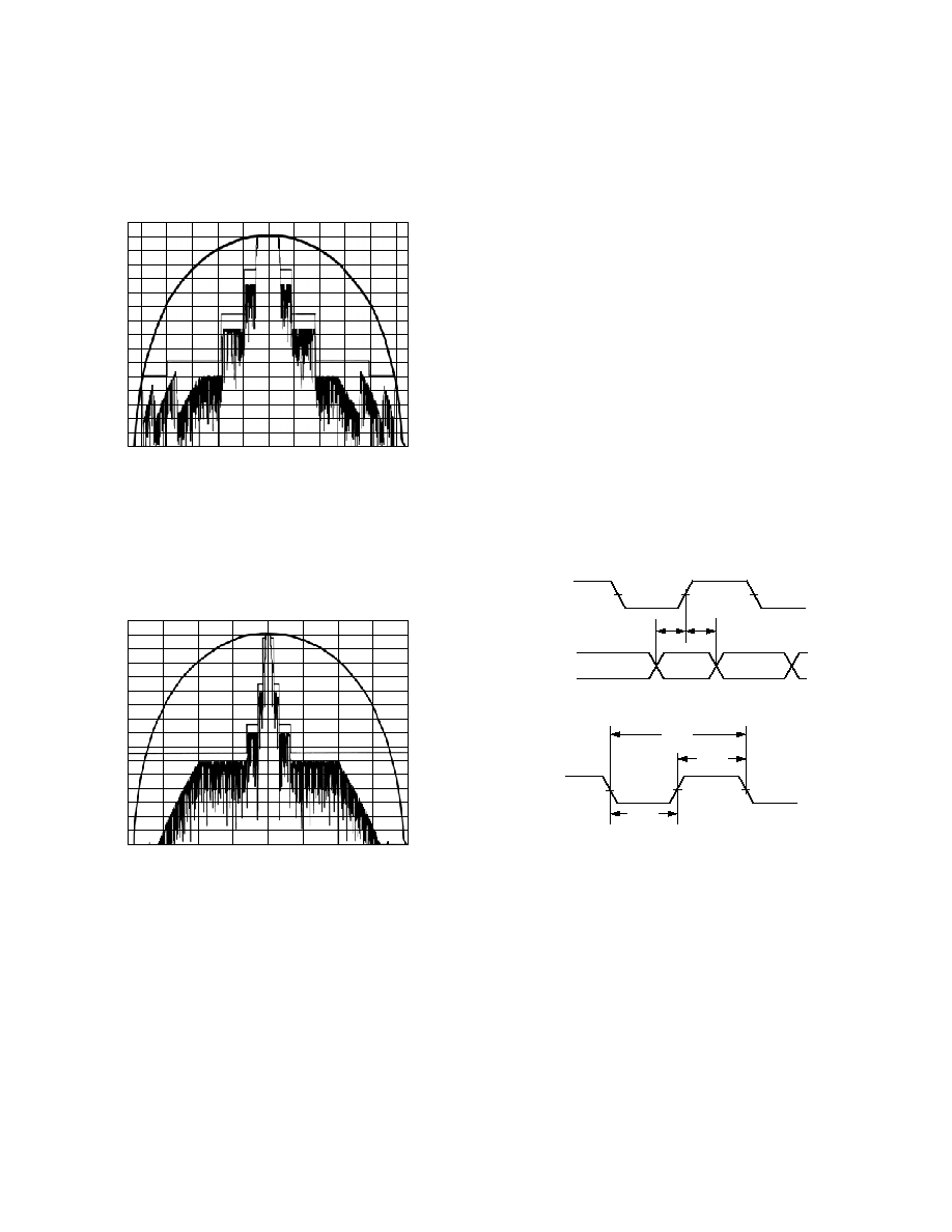
The filter in Figure 19 is based on a 65 MSPS input data rate
and an output rate of 541.6666 kSPS (two samples per symbol
for EDGE). Total decimation rate is 120 distributed between
the rCIC2, CIC5 and RCF.
kHz
10
1000
1000
dBc
800 600 400 200
0
200
400
600
800
0
50
20
40
10
30
60
0
80
100
70
90
110
120
140
130
150
Figure 19. Filter Response
The filter in Figure 20 is designed to meet the IS-136 specifica-
tions. For this configuration, the clock is set to 61.44 MSPS
with a total decimation rate of 320 providing an output data
rate of 192 kSPS or four samples per symbol.
kHz
10
dBc
500
400
200
0
200
400
500
0
50
20
40
10
30
60
0
80
100
70
90
110
120
140
130
150
Figure 20. Filter Response
INPUT DATA PORTS
The AD6624A features dual, high-speed ADC input ports, Input
Port A and Input Port B. The dual input ports allow for the
most flexibility with a single tuner chip. These can be diversity
inputs or truly independent inputs such as separate antenna
segments. Either ADC port can be routed to one of four tuner
channels. For added flexibility, each input port can be used to
support multiplexed inputs such as found on the AD6600 or
other ADCs with mixed outputs. This added flexibility can
allow for up to four different analog sources to be processed
simultaneously by the four internal channels.
In addition, the front end of the AD6624A contains circuitry that
enables high-speed signal level detection and control. This is
accomplished with a unique high-speed level detection circuit
that offers minimal latency and maximum flexibility to control
up to four analog signal paths. The overall signal path latency
from input to output on the AD6624A can be expressed in high-
speed clock cycles. The equation below can be used to calculate
the latency.
T
M
M
N
SDIV
LATENCY
rC C
CIC
TAPS
=
+
(
)
+
+
+
(
)
+
1 2
5
7
4
1
18
M
rC1C2
and M
CIC5
are decimation values for the rC1C2 and
CIC5 filters respectively, N
TAPS
is the number RCF taps chosen,
and SDIV is the chosen SCLK divisor factor.
Input Data Format
Each input port consists of a 14-bit mantissa and 3-bit exponent. If
interfacing to a standard ADC is required, the exponent bits can
be grounded. If connected to a floating point ADC such as the
AD6600, the exponent bits from that product can be connected
to the input exponent bits of the AD6624A. The mantissa data
format is two's-complement and the exponent is unsigned binary.
Input Timing
The data from each high-speed input port is latched on the
rising edge of CLK. This clock signal is used to sample the
input port and clock the synchronous signal processing stages
that follow in the selected channels.
The clock signals can operate up to 80 MHz and have a 50% duty
cycle. In applications using high-speed ADCs, the ADC sample
clock or data valid strobe is typically used to clock the AD6624A.
CLK
IN[13:0]
EXP[2:0]
DATA
t
SI
t
HI
Figure 21. Input Data Timing Requirements
CLK
t
CLK
t
CLKH
t
CLKL
Figure 22. CLK Timing Requirements
Input Enable Control
There is an IENA and an IENB pin for the Input Port A and
Input Port B respectively. There are four modes of operation
used for each IEN pin. Using these modes, it is possible to
emulate operation of the other RSPs such as the AD6620, which
offer dual channel modes normally associated with diversity
operations. These modes are: IEN transition to low, IEN transi-
tion to high, IEN high, and blank on IEN low.
In the IEN high mode, the inputs and normal operations occur
when the Input Enable is high. In the IEN transition to low
mode, normal operations occur on the first rising edge of the
clock after the IEN transitions to low. Likewise, in the IEN
transition to high mode, operations occur on the rising edge of
the clock after the IEN transitions to high. See the Numerically
Controlled Oscillator section for more details on configuring the
Input Enable Modes. In blank on IEN low mode, the input data
is interpreted as zero when IEN is low.

REV. 0
AD6624A
15
A typical application for this feature would be to take the data
from an AD6600 Diversity ADC to one of the inputs of the
AD6624A. The A/B_OUT from that chip would be tied to the
IEN. One channel within the AD6624A would be then set so
that IEN transition to low is enabled. Another channel would be
configured so that IEN transition to high is enabled. One of the
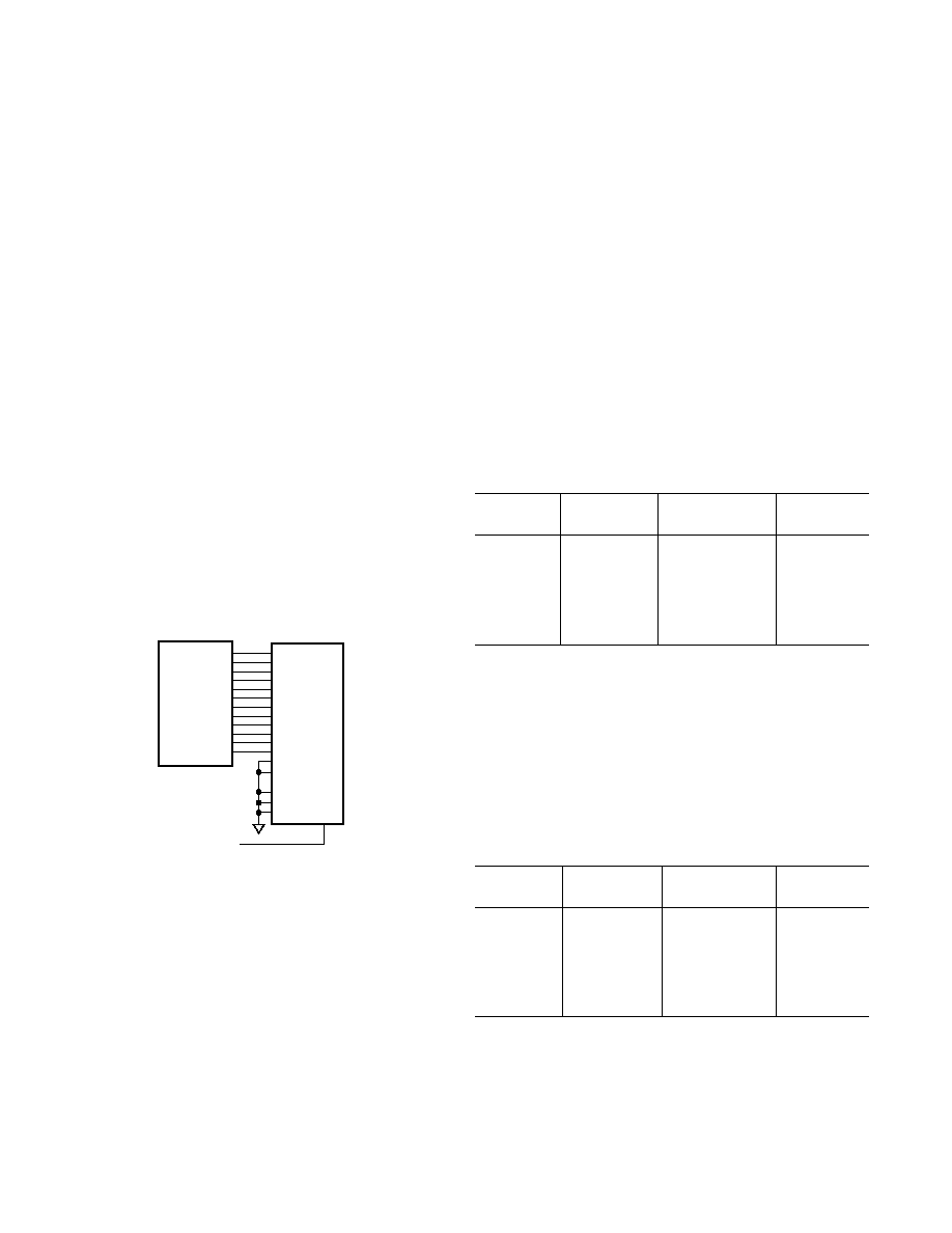
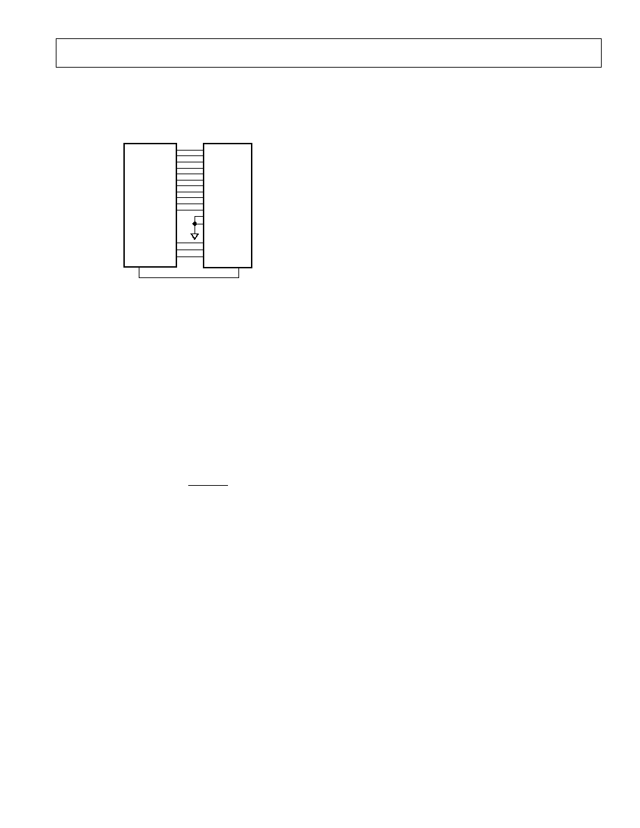
serial outputs would be configured as the Serial Bus Master and
the other as a serial bus slave and the output bus configured as
shown in Figure 25. This would allow two of the AD6624A
channels to be configured to emulate that AD6620 in diversity
mode. Of course the NCO frequencies and other channel char-
acteristics would need to be set similarly, but this feature allows
the AD6624A to handle interleaved data streams such as found
on the AD6600.
The difference between the IEN transition to high and the IEN
high is found when a system clock is provided that is higher than
the data rate of the converter. It is often advantageous to supply
a clock that runs faster than the data rate so that additional filter
taps can be computed. This naturally provides better filtering.
In order to ensure that other parts of the circuit properly recog-
nize the faster clock in the simplest manner, the IEN transition
to low or high should be used. In this mode, only the first clock
edge that meets the setup and hold times will be used to latch
and process the input data. All other clock pulses are ignored by
front end processing. However, each clock cycle will still pro-
duce a new filter computation pair.
Gain Switching
The AD6624A includes circuitry that is useful in applications
where either large dynamic ranges exist or where gain ranging
converters are employed. This circuitry allows digital thresh-
olds to be set such that an upper and a lower threshold can
be programmed.
One such use of this may be to detect when an ADC converter
is about to reach full-scale with a particular input condition.
The result would be to provide a flag that could be used to
quickly insert an attenuator that would prevent ADC overdrive.
If 18 dB (or any arbitrary value) of attenuation (or gain) is
switched in, the signal dynamic range of the system will have
been increased by 18 dB. The process begins when the input
signal reaches the upper programmed threshold. In a typical
application, this may be set 1 dB (user-definable) below full-
scale. When this input condition is met, the appropriate LI
(LIA-A, LIA-B, LIB-A, or LIB-B) signal associated with either
the A or B input port is made active. This can be used to switch
the gain or attenuation of the external circuit. The LI signal stays
active until the input condition falls below the lower programmed
threshold. To provide hysteresis, a dwell-time register (see
Memory Map for Input Control Registers) is available to hold
off switching of the control line for a predetermined number of
clocks. Once the input condition is below the lower thresh-
old, the programmable counter begins counting high-speed
clocks. As long as the input signal stays below the lower thresh-
old for the number of high-speed clock cycles programmed, the
attenuator will be removed on the terminal count. However, if
the input condition goes above the lower threshold with the
counter running, it will be reset and must fall below the lower
threshold again to initiate the process. This will prevent unnec-
essary switching between states.
This is illustrated in Figure 23. When the input signal goes
above the upper threshold, the appropriate LI signal becomes
active. Once the signal falls below the lower threshold, the
counter begins counting. If the input condition goes above the
lower threshold, the counter is reset and starts again as shown
in Figure 23. Once the counter has terminated to zero, the LI
signal goes inactive.
"HIGH"
DWELL TIME
"LOW"
TIME
UPPER THRESHOLD
LOWER THRESHOLD
COUNTER RESTARTS
Figure 23. Threshold Settings for LI
The LI signal can be used for a variety of functions. It can be
used to set the controls of an attenuator DVGA or integrated and
used with an analog VGA. To simplify the use of this feature,
the AD6624A includes two separate gain settings, one when this
line is inactive (rCIC2_QUIET[4:0]) and the other when active
(rCIC2_LOUD[4:0]). This allows the digital gain to be adjusted
to the external changes. In conjunction with the gain setting, a
variable hold-off is included to compensate for the pipeline delay of
the ADC and the switching time of the gain control element.
Together, these two features provide seamless gain switching.
Another use of these pins is to facilitate a gain range hold-off within
a gain-ranging ADC. For converters that use gain ranging to
increase total signal dynamic range, it may be desirable to pro-
hibit internal gain ranging from occurring in some instances.
For such converters, the LI (A or B) signals can be used to hold
this off. For this application, the upper threshold would be set
based on similar criteria. However, the lower threshold would
be set to a level consistent with the gain ranges of the specific
converter. The hold-off delay can then be set appropriately for
any number of factors such as fading profile, signal peak to
average ratio, or any other time-based characteristics that might
cause unnecessary gain changes.
Since the AD6624A has a total of four gain control circuits that
can be used if both A and B Input Ports have interleaved data,
each respective LI pin is independent and can be set to different
set points. It should be noted that the gain control circuits are
wideband and are implemented prior to any filtering elements to
minimize loop delay. Any of the four channels can be set to
monitor any of the possible four input channels (two in normal
mode and four when the inputs are time-multiplexed).
The chip also provides appropriate scaling of the internal data
based on the attenuation associated with the LI signal. In this
manner, data to the DSP maintains a correct scale value through-
out the process, making it totally independent. Since finite
delays are often associated with external gain switching compo-
nents, the AD6624A includes a variable pipeline delay that can
be used to compensate for external pipeline delays or gross
settling times associated with gain/attenuator devices. This delay
may be set up to seven high-speed clocks. These features ensure
smooth switching between gain settings.

REV. 0
AD6624A
16
The RSSI output of the AD6600 numerically grows with increasing
signal strength of the analog input (RSSI = 5 for a large signal,
RSSI = 0 for a small signal). When the Exponent Invert Bit
(ExpInv) is set to zero, the AD6624A will consider the smallest
signal at the IN[13:0] to be the largest and as the EXP word
increases, it shifts the data down internally (EXP = 5 will shift a
14-bit word right by five internal bits before passing the data to
the rCIC2). In this example, where ExpInv = 0, the AD6624A
regards the largest signal possible on the AD6600 as the smallest
signal. Thus, the Exponent Invert Bit can be used to make the
AD6624A exponent agree with the AD6600 RSSI. By setting
ExpInv = 1, it forces the AD6624A to shift the data up (left) for
growing EXP instead of down. The exponent invert bit should
always be set high for use with the AD6600.
The Exponent Offset is used to shift the data right. For example,
Table I shows that with no rCIC2 scaling, 12 dB of range is lost
when the ADC input is at the largest level. This is undesirable
because it lowers the Dynamic Range and SNR of the system by
reducing the signal of interest relative to the quantization noise floor.
Table I. AD6600 Transfer Function with AD6624A ExpInv = 1,
and No ExpOff
ADC Input
AD6600
AD6624A
Signal
Level
RSSI[2:0]
Data
Reduction
Largest
101 (5)
4 (>> 2)
12 dB
100 (4)
8 (>> 3)
18 dB
011 (3)
16 (>> 4)
24 dB
010 (2)
32 (>> 5)
30 dB
001 (1)
64 (>> 6)
36 dB
Smallest
000 (0)
128 (>> 7)
42 dB
(ExpInv = 1, ExpOff = 0)
To avoid this automatic attenuation of the full-scale ADC
signal, the ExpOff is used to move the largest signal (RSSI = 5)
up to the point where there is no downshift. In other words,
once the Exponent Invert bit has been set, the Exponent Offset
should be adjusted so that mod(75 + ExpOff,8) = 0. This is
the case when Exponent Offset is set to 6 since mod(8,8) = 0.
Table II illustrates the use of ExpInv and ExpOff when used
with the AD6600 ADC.
Table II. AD6600 Transfer Function with AD6624A ExpInv = 1,
and ExpOff = 6
ADC Input
AD6600
AD6624A
Signal
Level
RSSI[2:0]
Data
Reduction
Largest
101 (5)
1 (>> 0)
0 dB
100 (4)
2 (>> 1)
6 dB
011 (3)
4 (>> 2)
12 dB
010 (2)
8 (>> 3)
18 dB
001 (1)
16 (>> 4)
24 dB
Smallest
000 (0)
32 (>> 5)
30 dB
(ExpInv = 1, ExpOff = 6)
This flexibility in handling the exponent allows the AD6624A
to interface with gain-ranging ADCs other than the AD6600.
The Exponent Offset can be adjusted to allow up to seven
RSSI(EXP) ranges to be used as opposed to the AD6600's five.
Input Data Scaling
The AD6624A has two data input ports: an A Input Port and a
B Input Port. Each accepts 14-bit mantissa (two's-complement
integer) IN[13:0], a 3-bit exponent (unsigned integer) EXP[2:0]
and the Input Enable (IEN). Both inputs are clocked by CLK.
These pins allow direct interfacing to both standard fixed-point
ADCs such as the AD9225 and AD6640, as well as to gain-
ranging ADCs such as the AD6600. For normal operation with
ADCs having fewer than 14 bits, the active bits should be MSB-
justified and the unused LSBs should be tied low.
The 3-bit exponent, EXP[2:0], is interpreted as an unsigned
integer. The exponent will subsequently be modified by either of
the 5-bit scale values stored in register 0x92, Bits 40 or Bits 95.
These 5-bit registers contain the sum of the rCIC2 scale value plus
the external attenuator scale settings and the Exponent Offset
(ExpOff). If no external attenuator is used, these values can only
be set to the value of the rCIC2 scale. If an external attenuator is
used, Bit Position 40 (Register 0x92 rCIC2_LOUD[4:0]) con-
tains the scale value for the largest input range. Bit Positions
95 (Register 0x92 rCIC2_QUIET[4:0]) are used for the nonat-
tenuated input signal range.
Scaling with Fixed-Point ADCs
For fixed-point ADCs, the AD6624A exponent inputs EXP[2:0]
are typically not used and should be tied low. The ADC outputs
are tied directly to the AD6624A Inputs, MSB-justified. The
ExpOff bits in 0x92 should be programmed to 0. Likewise, the
Exponent Invert bit should be 0.
Thus for fixed-point ADCs, the exponents are typically static
and no input scaling is used in the AD6624A.
D11 (MSB)
AD6640
D0 (LSB)
AD6624A
IN13
IN2
IN1
IN0
IEN
EXP2
EXP1
EXP0
VDD
NOTE:
EXPOFF = 0, EXPINV = 0
Figure 24. Typical Interconnection of the AD6640 Fixed
Point ADC and the AD6624A
Scaling with Floating-Point or Gain-Ranging ADCs
An example of the exponent control feature combines the AD6600
and the AD6624A. The AD6600 is an 11-bit ADC with three bits
of gain ranging. In effect, the 11-bit ADC provides the mantissa,
and the three bits of relative signal strength indicator (RSSI) for
the exponent. Only five of the eight available steps are used by
the AD6600. See the AD6600 data sheet for additional details.
For gain-ranging ADCs such as the AD6600,
scaled input
IN
ExpInv
ExpWeight
Exp rCIC
_
,
,
mod(
, )
=
×
=
=
+
2
1
0
7
2 8
(1)
where: IN is the value of IN[13:0], Exp is the value of EXP[2:0],
and rCIC2 is the rCIC scale register value (0x92 Bits 95 and 40).

REV. 0
AD6624A
17
It also allows the AD6624A to be tailored in a system that employs
the AD6600, but does not utilize all of its signal range. For
example, if only the first four RSSI ranges are expected to occur,
the ExpOff could be adjusted to five, which would then make
RSSI = 4 correspond to the 0 dB point of the AD6624A.
D10 (MSB)
AD6600
D0 (LSB)
AD6624A
IN13
IN2
IN1
IN0
IEN
EXP2
EXP1
EXP0
RSSI2
RSSI1
RSSI0
AB_OUT
Figure 25. Typical Interconnection of the AD6600 Gain-
Ranging ADC and the AD6624A
NUMERICALLY CONTROLLED OSCILLATOR
Frequency Translation
This processing stage comprises a digital tuner consisting of two
multipliers and a 32-bit complex NCO. Each channel of the
AD6624A has an independent NCO. The NCO serves as a
quadrature local oscillator capable of producing an NCO frequency
between CLK/2 and +CLK/2 with a resolution of CLK/2
32
in the
complex mode. The worst-case spurious signal from the NCO is
better than 100 dBc for all output frequencies.
The NCO frequency value in registers 0x85 and 0x86 are inter-
preted as a 32-bit unsigned integer. The NCO frequency is
calculated using the equation below.
NCO FREQ
f
CLK
CHANNEL
_
mod
=
×
2
32
(2)
NCO_FREQ is the 32-bit integer (Registers 0x85 and 0x86),
f
CHANNEL
is the desired channel frequency, and
CLK
* is the AD6624A master clock rate (CLK).
NCO Frequency Hold-Off Register
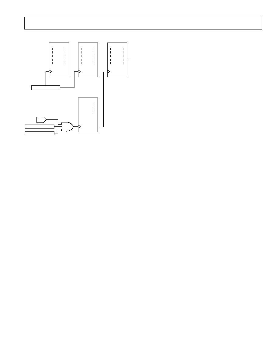
When the NCO Frequency registers are written, data is actually
passed to a shadow register. Data may be moved to the main
registers by one of two methods. The first is to start the chip
using the soft sync feature, which will directly load the NCO
registers. The second allows changes to be pre-written and then
updated through direct software control. To accomplish this,
there is an NCO Frequency Hold-Off Counter. The counter
(0x84) is a 16-bit unsigned integer and is clocked at the master
CLK rate. This hold-off counter is also used in conjunction with
the frequency hopping feature of this chip.
Phase Offset
The phase offset register (0x87) adds an offset to the phase
accumulator of the NCO. This is a 16-bit register and is inter-
preted as a 16-bit unsigned integer. A 0x0000 in this register
corresponds to a 0 radian offset and a 0xFFFF corresponds to
an offset of 2
(11/(2
16
)) radians. This register allows multiple
NCOs to be synchronized to produce sine waves with a known
and steady phase difference.
NCO Control Register
The NCO control register located at 0x88 is used to configure
the features of the NCO. These are controlled on a per-channel
basis. These are described below.
Bypass
The NCO in the front end of the AD6624A can be bypassed.
Bypass mode is enabled by setting Bit 0 of 0x88 high. When
they are bypassed, down conversion is not performed and the
AD6624A channel functions simply as a real filter on complex
data. This is useful for passband sampling application where the
A input is connected to the I signal path within the filter and the
B input is connected to the Q signal path. This may be desired if
the digitized signal has already been converted to passband in
prior analog stages or by other digital preprocessing.
Phase Dither
The AD6624A provides a phase dither option for improving the
spurious performance of the NCO. Phase dither is enabled by
setting Bit 1. When phase dither is enabled by setting this bit
high, spurs due to phase truncation in the NCO are randomized.
The energy from these spurs is spread into the noise floor and
Spurious Free Dynamic Range is increased at the expense of
very slight decreases in the SNR. The choice of whether phase
dither is used in a system will ultimately be decided by the system
goals. If lower spurs are desired at the expense of a slightly raised
noise floor, it should be employed. If a low noise floor is desired
and the higher spurs can be tolerated or filtered by subsequent
stages, phase dither is not needed.
Amplitude Dither
Amplitude dither can also be used to improve spurious perfor-
mance of the NCO. Amplitude dither is enabled by setting Bit 2.
Amplitude dither improves performance by randomizing the
amplitude quantization errors within the angular to Cartesian
conversion of the NCO. This option may reduce spurs at the
expense of a slightly raised noise floor. Amplitude dither and
phase dither can be used together, separately, or not at all.
Clear Phase Accumulator on HOP
When Bit 3 is set, the NCO phase accumulator is cleared prior
to a frequency hop. This ensures a consistent phase of the NCO
on each hop. The NCO phase offset is unaffected by this setting
and is still in effect. If phase-continuous hopping is desired, this
bit should be cleared and the last phase in the NCO phase regis-
ter will be the initiating point for the new frequency.
Input Enable Control
There are four different modes of operation for the input enable.
Each of the high-speed input ports includes an IEN line. Any of
the four filter channels can be programmed to take data from
either of the two A or B Input Ports (see WB Input Select section).
Along with data is the IEN(A, B) signal. Each filter channel can
be configured to process the IEN signal in one of four modes.
Three of the modes are associated with when data is processed
based on a time division multiplexed data stream. The fourth
mode is used in applications that employ time division duplex
such as radar, sonar, ultrasound, and communications that
involve TDD.
Mode 00: Blank On IEN Low
In this mode, data is blanked while the IEN line is low. During the
period of time when the IEN line is high, new data is strobed
on each rising edge of the input clock. When the IEN line is
*See NCO Mode Control section.

REV. 0
AD6624A
18
lowered, input data is replaced with zero values. During this
period, the NCO continues to run such that when the IEN line
is raised again, the NCO value will be at the value it would have
otherwise been in had the IEN line never been lowered. This
mode has the effect of blanking the digital inputs when the IEN
line is lowered. Back end processing (rCIC2, CIC5, and RCF)
continues while the IEN line is high. This mode is useful for
time division multiplexed applications.
Mode 01: Clock On IEN High
In this mode, data is clocked into the chip while the IEN line is
high. During the period of time when the IEN line is high, new
data is strobed on each rising edge of the input clock. When
IEN line is lowered, input data is no longer latched into the
channel. Additionally, NCO advances are halted. However,
back end processing (rCIC2, CIC5, and RCF) continues during
this period. The primary use for this mode is to allow for a clock
that is faster than the input sample data rate to allow more filter
taps to be computed than would otherwise be possible. In Fig-
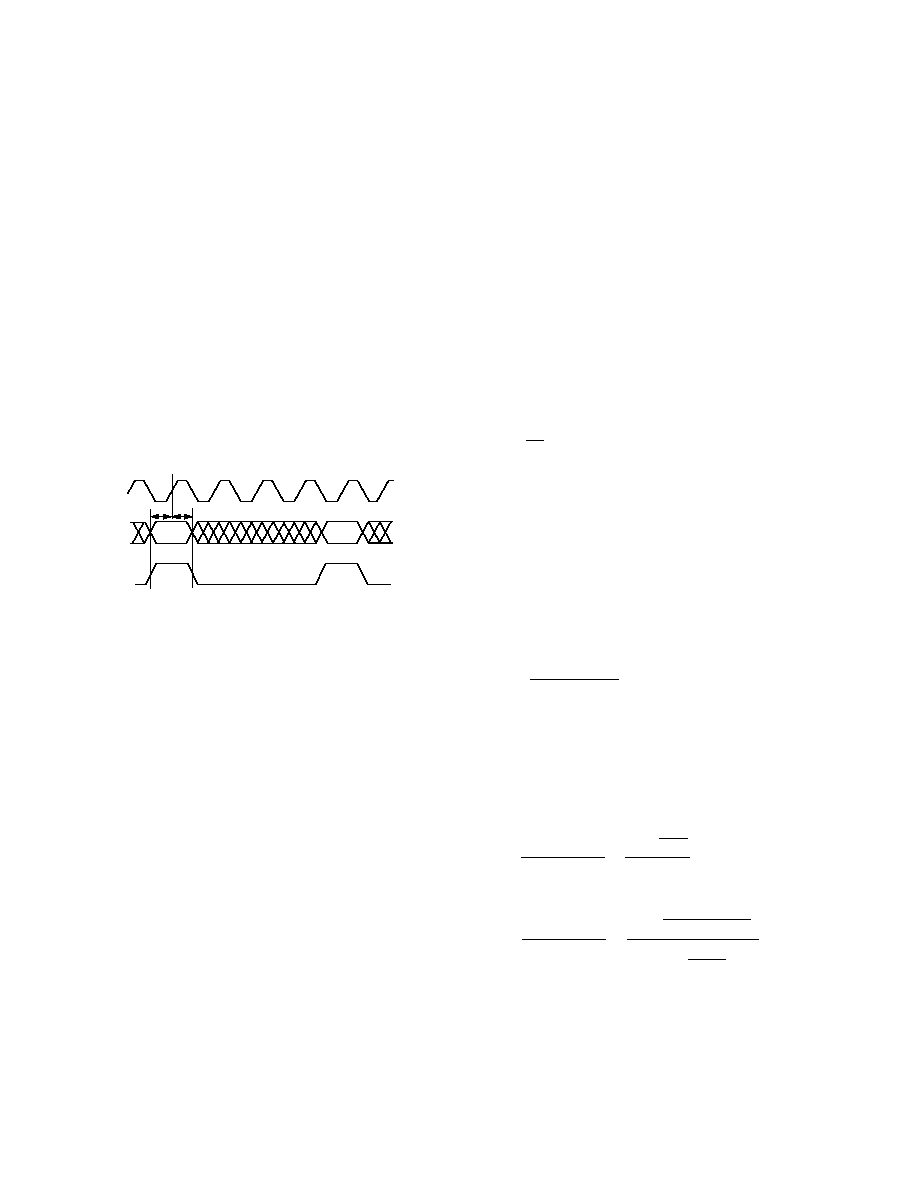
ure 26, input data is strobed only during the period of time when
IEN is high, despite the fact that the CLK continues to run at a
rate four times faster than the data.
CLK
t
HI
t
SI
n+1
n
IN[13:0]
E[2:0]
IEN
Figure 26. Fractional Rate Input Timing (4
× CLK) in
Mode 01
Mode 10: Clock on IEN Transition to High
In this mode, data is clocked into the chip only on the first clock
edge after the rising transition of the IEN line. Although data is
only latched on the first valid clock edge, the back end process-
ing (rCIC2, CIC5, and RCF) continues on each available clock
that may be present, similar to Mode 01. The NCO phase accu-
mulator is incremented only once for each new input data sample
and not once for each input clock.
Mode 11: Clock on IEN Transition to Low
In this mode, data is clocked into the chip only on the first clock
edge after the falling transition of the IEN line. Although data is
only latched on the first valid clock edge, the back end process-
ing (rCIC2, CIC5, and RCF) continues on each available clock
that may be present, similar to Mode 01. The NCO phase accu-
mulator is incremented only once for each new input data sample
and not once for each input clock.
WB Input Select
Bit 6 in this register controls which input port is selected for
signal processing. If this bit is set high, Input Port B (INB,
EXPB, and IENB) is connected to the selected filter channel. If
this bit is cleared, Input Port A (INA, EXPA, and IENA) is
connected to the selected filter channel.
Sync Select
Bits 7 and 8 of this register determine which external sync pin is
associated with the selected channel. The AD6624A has four sync
pins named SYNCA, SYNCB, SYNCC, and SYNCD. Any of
these sync pins can be associated with any of the four receiver
channels within the AD6624A. Additionally, if only one sync
signal is required for the system, all four receiver channels can
reference the same sync pulse. Bit value 00 is Channel A, 01 is
Channel B, 10 is Channel C, and 11 is Channel D.
SECOND ORDER rCIC FILTER
The rCIC2 filter is a second order cascaded resampling integra-
tor comb filter. The resampler is implemented using a unique
technique, which does not require the use of a high-speed clock,
thus simplifying the design and saving power. The resampler
allows for noninteger relationships between the master clock
and the output data rate. This allows easier implementation of
systems that are either multimode or require a master clock that
is not a multiple of the data rate to be used.
Interpolation up to 512, and decimation up to 4096, is allowed
in the rCIC2. The resampling factor for the rCIC2 (L) is a 9-bit
integer. When combined with the decimation factor M, a 12-bit
number, the total rate change can be any fraction in the form of:
R
L
M
R
rCIC
rCIC
2
2
1
=
(3)
The only constraint is that the ratio L/M must be less than or
equal to one. This implies that the rCIC2 decimates by 1 or more.
Resampling is implemented by apparently increasing the input
sample rate by the Factor L, using zero stuffing for the new data
samples. Following the resampler is a second order cascaded
integrator comb filter. Filter characteristics are determined only
by the fractional rate change (L/M).
The filter can process signals at the full rate of the input port
80 MHz. The output rate of this stage is given by Equation 4.
f
L
f
M
SAMP
rCIC
SAMP
rCIC
2
2
2
=
×
(4)
Both L
rCIC2
and M
rCIC2
are unsigned integers. The interpolation
rate (L
rCIC2
) may be from 1 to 512 and the decimation (M
rCIC2
)
may be between 1 and 4096. The stage can be bypassed by
setting the decimation to 1/1.
The frequency response of the rCIC2 filter is given by Equation 5.
H z
L
z
z
H f
L
M
f
L
f
f
f
S
rCIC
M
L
S
rCIC
rCIC
rCIC
SAMP
SAMP
rCIC
rCIC
rCIC
rCIC
( )
( )
sin
sin
=
×
×
-
-
=
×
×
×
×
-
1
2
1
1
1
2
2
2
2
2
2
1
2
2
2
2
2
(5)
The scale factor, S
rCIC2
is a programmable, unsigned 5-bit value
between 0 and 31. This serves as an attenuator that can reduce
the gain of the rCIC2 in 6 dB increments. For the best dynamic
range, S
rCIC2
should be set to the smallest value possible (i.e.,
lowest attenuation) without creating an overflow condition.
This can be safely accomplished using the following equation:

REV. 0
AD6624A
19
where input_level is the largest fraction of full-scale possible at
the input to the AD6624A (normally 1). The rCIC2 scale factor
is always used whether or not the rCIC2 is bypassed.
Moreover, there are two scale registers (rCIC2_LOUD[4:0]
Bits 40 in x92), and (rCIC2_QUIET[4:0] Bits 95 in 0x92)
that are used in conjunction with the computed S
rCIC2
which
determines the overall rCIC2 scaling. The S
rCIC2
value must
be summed with the values in each respective scale register and
ExpOff, to determine the scale value that must be placed in the
rCIC2 scale register. This number must be less than 32 or the
interpolation and decimation rates must be adjusted to validate
this equation. The ceil function denotes the next whole integer
and the floor function denotes the previous whole integer. For
example, the ceil(4.5) is 5 while the floor(4.5) is 4.
The gain and passband droop of the rCIC2 should be calculated
by the equations above, as well as the filter transfer equations that
follow. Excessive passband droop can be compensated for in the
RCF stage by peaking the passband by the inverse of the roll-off.
scaled
input
IN
ExpInv
scaled
input
IN
ExpInv
Exp
rCIC
Exp
rCIC
_
,
_
,
mod(
, )
mod(
, )
=
×
=
=
×
=
-
+
-
-
+
2
0
2
1
2 8
7
2 8
(7)
where: IN is the value of IN[15:0], Exp is the value of EXP[2:0],
and rCIC2 is the value of the 0x92 (rCIC2_QUIET[4:0] and
rCIC2_LOUD[4:0]) scale register.
rCIC2 Rejection
Table III illustrates the amount of bandwidth in percent of the
data rate into the rCIC2 stage. The data in this table may be
scaled to any other allowable sample rate up to 80 MHz in
Single Channel Mode or 40 MHz in Diversity Channel Mode.
The table can be used as a tool to decide how to distribute the
decimation between rCIC2, CIC5, and the RCF.
Table III. SSB rCIC2 Alias Rejection Table (f
SAMP
= 1)
Bandwidth Shown in Percentage of f
SAMP
M
CIC5
/
L
rCIC2
50 dB 60 dB
70 dB
80 dB 90 dB
100 dB
2
1.79
1.007
0.566
0.318
0.179
0.101
3
1.508
0.858
0.486
0.274
0.155
0.087
4
1.217
0.696
0.395
0.223
0.126
0.071
5
1.006
0.577
0.328
0.186
0.105
0.059
6
0.853
0.49
0.279
0.158
0.089
0.05
7
0.739
0.425
0.242
0.137
0.077
0.044
8
0.651
0.374
0.213
0.121
0.068
0.038
9
0.581
0.334
0.19
0.108
0.061
0.034
10
0.525
0.302
0.172
0.097
0.055
0.031
11
0.478
0.275
0.157
0.089
0.05
0.028
12
0.439
0.253
0.144
0.082
0.046
0.026
13
0.406
0.234
0.133
0.075
0.043
0.024
14
0.378
0.217
0.124
0.07
0.04
0.022
15
0.353
0.203
0.116
0.066
0.037
0.021
16
0.331
0.19
0.109
0.061
0.035
0.02
Example Calculations
Goal: Implement a filter with an Input Sample Rate of 10 MHz
requiring 100 dB of alias rejection for a
±7 kHz passband.
Solution: First determine the percentage of the sample rate that
is represented by the passband.
BW
kHz
MHz
FRACTION
=
×
=
100
7
10
0 07
.
(8)
Find the 100 dB column in Table III and look down this column
for a value greater than or equal to your passband percentage of
the clock rate. Then look across to the extreme left column and
find the corresponding rate-change factor (M
rCIC2
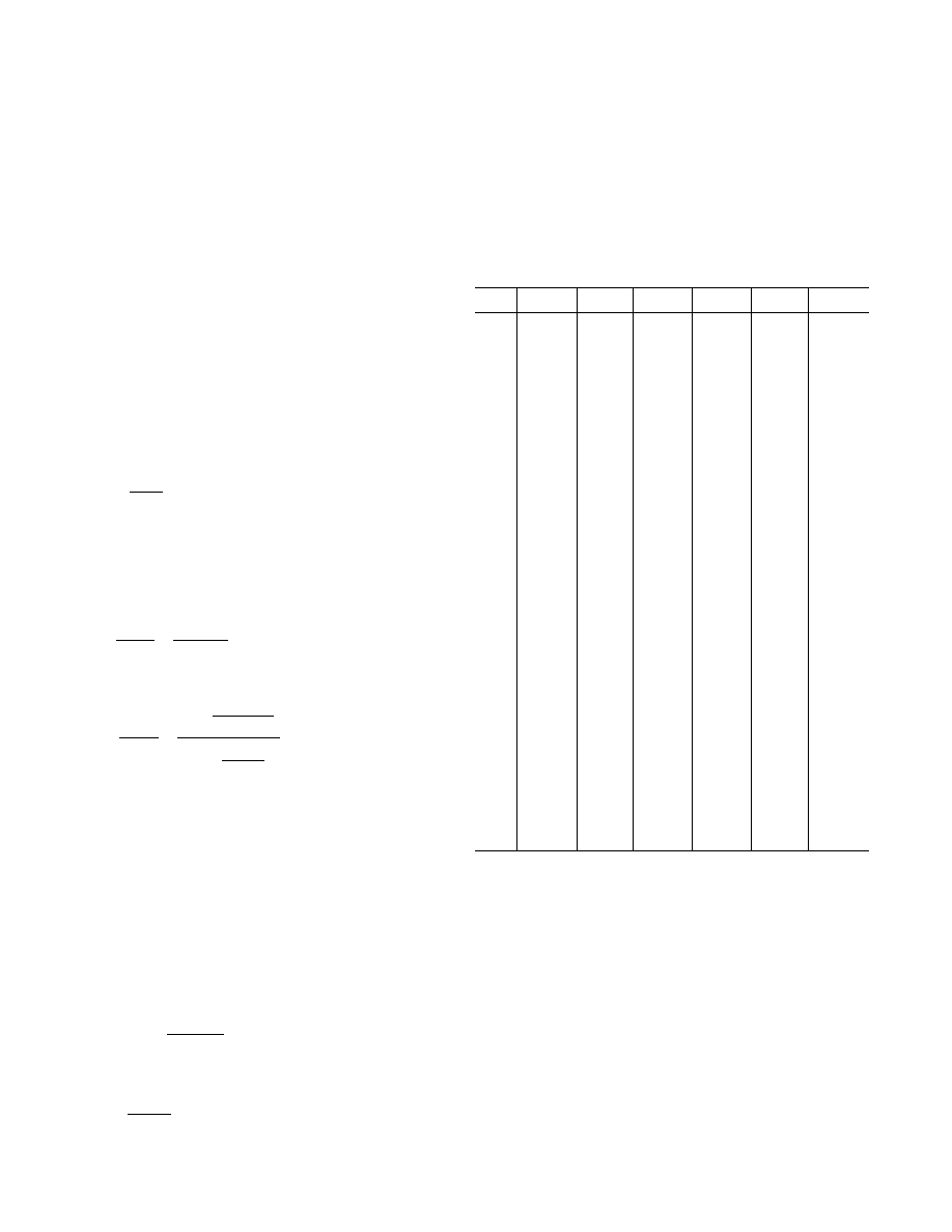
/L
rCIC2
). Refer-
ring to the table, notice that for a M
rCIC2
/L
rCIC2
of 4, the frequency
having 100 dB of alias rejection is 0.071 percent, which is
slightly greater than the 0.07 percent calculated. Therefore, for
this example, the maximum bound on rCIC2 rate change is 4.
A higher chosen M
rCIC2
/L
rCIC2
means less alias rejection than
the 100 dB required.
An M
rCIC2
/L
rCIC2
of less than four would still yield the required
rejection; however, the power consumption can be minimized
by decimating as much as possible in this rCIC2 stage. Decima-
tion in rCIC2 lowers the data rate, and thus reduces power
consumed in subsequent stages. It should also be noted that
there is more than one way to determine the decimation by 4. A
decimation of 4 is the same as an L/M ratio of 0.25. Thus any
integer combination of L/M that yields 0.25 will work (1/4, 2/8,
or 4/16). However, for the best dynamic range, the simplest
ratio should be used. For example, 1/4 gives better performance
than 4/16.
Decimation and Interpolation Registers
rCIC2 decimation values are stored in register 0x90. This is a
12-bit register and contains the decimation portion less 1. The
interpolation portion is stored in register 0x91. This 9-bit value
holds the interpolation less one.
rCIC2 Scale
Register 0x92 contains the scaling information for this section of
the circuit. The primary function is to store the scale value
computed in the sections above.
Bits 40 (rCIC2_LOUD[4:0]) of this register are used to con-
tain the scaling factor for the rCIC2 during conditions of strong
signals. These five bits represent the rCIC2 scalar calculated above
plus any external signal scaling with an attenuator.
Bits 95 (rCIC2_QUIET[4:0]) of this register are used to con-
tain the scaling factor for the rCIC2 during conditions of weak
signals. In this register, no external attenuator would be used
and is not included. Only the value computed above is stored in
these bits.
Bit 10 of this register is used to indicate the value of the external
exponent. If this bit is set LOW, each external exponent repre-
sents 6 dB per step as in the AD6600. If this bit is set to HIGH,
each exponent represents a 12 dB step.
S
ceil
M
floor
M
L
M
L
floor
M
L
OL
M
L
input level
rCIC
rCIC
rCIC
rCIC
rCIC
rCIC
rCIC
rCIC
CIC
rCIC
rCIC
S
rCIC
2
2
2
2
2
2
2
2
2
2
2
2
2
2
1
2
2
=
+
×
×
-
×
+
=
×
×
log
(
)
_
(6)

REV. 0
AD6624A
20
Bit 11 of this register is used to invert the external exponent
before internal calculation. This bit should be set HIGH for
gain-ranging ADCs that use an increasing exponent to represent
an increasing signal level. This bit should be set LOW for gain-
ranging ADCs that use a decreasing exponent for representing
an increasing signal level.
In applications that do not require the features of the rCIC2,
it may be bypassed by setting the L/M ratio to 1/1. This effectively
bypasses all circuitry of the rCIC2 except the scaling, which
is still effectual.
FIFTH ORDER CASCADED INTEGRATOR COMB FILTER
The third signal processing stage, CIC5, implements a sharper
fixed-coefficient, decimating filter than CIC2. The input rate to
this filter is f
SAMP2
. The maximum input rate is given by Equa-
tion 9. N
CH
equals two for Diversity Channel Real input mode;
otherwise N
CH
equals one. In order to satisfy this equation, M
CIC2
can be increased, N
CH
can be reduced, or f
CLK
can be increased
(reference fractional rate input timing described in the Input
Timing section).
f
f
N
SAMP
CLK
CH
2
(9)
The decimation ratio, M
CIC5
, may be programmed from 2 to 32
(all integer values). The frequency response of the filter is given
by Equation 10. The gain and passband droop of CIC5 should
be calculated by these equations. Both parameters may be com-
pensated for in the RCF stage.
H z
z
z
S
M
CIC
CIC
( )
=
×
+
1
2
1
1
5
5
5
1
5
(10)
H f
M
f
f
f
f
S
CIC
SAMP
SAMP
CIC
( )
sin
sin
=
×
×
+
1
2
5
5
5
2
2
5
The scale factor, S
CIC5
is a programmable unsigned integer
between 0 and 20. It serves to control the attenuation of the
data into the CIC5 stage in 6 dB increments. For the best
dynamic range, S
CIC5
should be set to the smallest value possible
(lowest attenuation) without creating an overflow condition.
This can be safely accomplished using Equation 11, where
OL
rCIC2
is the largest fraction of full scale possible at the input
to this filter stage. This value is output from the rCIC2 stage,
then pipelined into the CIC5.
S
ceil
M
OL
OL
M
OL
CIC
CIC
rCIC
CIC
CIC
S
rCIC
CIC
5
2
5
5
2
5
5
5
5
2
5
2
5
=
×
(
)
=
(
)
×
+
log (
)
(11)
The output rate of this stage is given by Equation 12.
f
f
M
SAMP
SAMP
CIC
5
2
5
(12)
CIC5 Rejection
Table IV illustrates the amount of bandwidth in percentage of
the clock rate that can be protected with various decimation
rates and alias rejection specifications. The maximum input rate
into the CIC5 is 80 MHz when the rC1C2 decimates by one.
As in Table III, these are the 1/2 bandwidth characteristics of
the CIC5. Note that the CIC5 stage can protect a much wider
band than the CIC2 for any given rejection.
Table IV. SSB CIC5 Alias Rejection Table (f
SAMP2
= 1)
M
CIC5
50 dB 60 dB
70 dB
80 dB 90 dB
100 dB
2
10.227
8.078
6.393
5.066
4.008
3.183
3
7.924
6.367
5.11
4.107
3.297
2.642
4
6.213
5.022
4.057
3.271
2.636
2.121
5
5.068
4.107
3.326
2.687
2.17
1.748
6
4.267
3.463
2.808
2.27
1.836
1.48
7
3.68
2.989
2.425
1.962
1.588
1.281
8
3.233
2.627
2.133
1.726
1.397
1.128
9
2.881
2.342
1.902
1.54
1.247
1.007
10
2.598
2.113
1.716
1.39
1.125
0.909
11
2.365
1.924
1.563
1.266
1.025
0.828
12
2.17
1.765
1.435
1.162
0.941
0.76
13
2.005
1.631
1.326
1.074
0.87
0.703
14
1.863
1.516
1.232
0.998
0.809
0.653
15
1.74
1.416
1.151
0.932
0.755
0.61
16
1.632
1.328
1.079
0.874
0.708
0.572
17
1.536
1.25
1.016
0.823
0.667
0.539
18
1.451
1.181
0.96
0.778
0.63
0.509
19
1.375
1.119
0.91
0.737
0.597
0.483
20
1.307
1.064
0.865
0.701
0.568
0.459
21
1.245
1.013
0.824
0.667
0.541
0.437
22
1.188
0.967
0.786
0.637
0.516
0.417
23
1.137
0.925
0.752
0.61
0.494
0.399
24
1.09
0.887
0.721
0.584
0.474
0.383
25
1.046
0.852
0.692
0.561
0.455
0.367
26
1.006
0.819
0.666
0.54
0.437
0.353
27
0.969
0.789
0.641
0.52
0.421
0.34
28
0.934
0.761
0.618
0.501
0.406
0.328
29
0.902
0.734
0.597
0.484
0.392
0.317
30
0.872
0.71
0.577
0.468
0.379
0.306
31
0.844
0.687
0.559
0.453
0.367
0.297
32
0.818
0.666
0.541
0.439
0.355
0.287
This table helps to calculate an upper bound on decimation,
M
CIC5
, given the desired filter characteristics.
RAM COEFFICIENT FILTER
The final signal processing stage is a sum-of-products decimat-
ing filter with programmable coefficients (see Figure 27). The
data memories I-RAM and Q-RAM store the 160 most recent
complex samples from the previous filter stage with 20-bit
resolution. The coefficient memory, CMEM, stores up to 256
coefficients with 20-bit resolution. On every CLK cycle, one tap
for I and one tap for Q are calculated using the same coefficients.
The RCF output consists of 24-bit data bits.

REV. 0
AD6624A
21
I IN
Q IN
160 20b
I-RAM
I OUT
256 20b
C-RAM
160 20b
Q-RAM
Q OUT
Figure 27. RAM Coefficient Filter Block Diagram
RCF Decimation Register
Each RCF channel can be used to decimate the data rate. The
decimation register is an 8-bit register and can decimate from 1
to 256. The RCF decimation is stored in 0xA0 in the form of
M
RCF
-1. The input rate to the RCF is f
SAMP5
.
RCF Decimation Phase
The RCF decimation phase can be used to synchronize multiple
filters within a chip. This is useful when using multiple channels
within the AD6624A to implement polyphase filter allowing the
resources of several filters to be operated in parallel and shared.
In such an application, two RCF filters would be processing the
same data from the CIC5. However, each filter will be delayed
by one-half the decimation rate, thus creating a 180
° phase
difference between the two halves. The AD6624A filter channel
uses the value stored in this register to preload the RCF counter.
Therefore, instead of starting from 0, the counter is loaded with
this value, thus creating an offset in the processing that should
be equivalent to the required processing delay. This data is
stored in 0xA1 as an 8-bit number.
RCF Filter Length
The maximum number of taps this filter can calculate, N
TAPS
, is
given by the equation below. The value N
TAPS
-1 is written to the
channel register within the AD6624A at address 0xA2.
N
f
M
f
TAPS
CLK
RCF
SAMP
×
min
5
160
,
(13)
The RCF coefficients are located in addresses 0x00 to 0x7F and
are interpreted as 20-bit two's-complement numbers. When
writing the coefficient RAM, the lower addresses will be mul-
tiplied by relatively older data from the CIC5, and the higher
coefficient addresses will be multiplied by relatively newer data
from the CIC5. The coefficients need not be symmetric and the
coefficient length, N
TAPS
, may be even or odd. If the coefficients
are symmetric, both sides of the impulse response must be written
into the coefficient RAM.
Although the base memory for coefficients is only 128 words
long, the actual length is 256 words long. There are two pages,
each of 128 words long. The page is selected by Bit 8 of 0xA4.
Although this data must be written in pages, the internal core
handles filters that exceed the length of 128 taps. Therefore,
the full length of the data RAM may be used as the filter
length (160 taps).
The RCF stores the data from the CIC5
into a 160
× 40 RAM.
160
× 20 is assigned to I data and 160 × 20 is assigned to Q
data. The RCF uses the RAM as a circular buffer, so that it is
difficult to know in which address a particular data element is
stored. To avoid start-up transients due to undefined data RAM
values, the data RAM should be cleared upon initialization.
When the RCF is triggered to calculate a filter output, it starts
by multiplying the oldest value in the data RAM by the first
coefficient, which is pointed to by the RCF Coefficient Offset
Register (0xA3). This value is accumulated with the products
of newer data words multiplied by the subsequent locations
in the coefficient RAM until the coefficient address RCF
OFF
+ N
TAPS
1 is reached.
Table V. Three-Tap Filter
Coefficient Address
Impulse Response
Data
0
h(0)
N(0) Oldest
1
h(1)
N(1)
2 (N
TAPS
1)
h(2)
N(2) Newest
The RCF Coefficient Offset register can be used for two purposes.
The main purpose of this register is to allow multiple filters to be
loaded into memory and selected simply by changing the offset
as a pointer for rapid filter changes. The other use of this register is
to form part of symbol timing adjustment. If the desired filter
length is padded with zeros on the ends, the starting point can
be adjusted to form slight delays when the filter is computed
with reference to the high-speed clock. This allows for vernier
adjustment of the symbol timing. Course adjustments can be made
with the RCF Decimation Phase.
The output rate of this filter is determined by the output rate of
the CIC5 stage and M
RCF
.
f
f
M
SAMPR
SAMP
RCF
=
5
(14)
RCF Output Scale Factor and Control Register
Register 0xA4 is a compound register used to configure several
aspects of the RCF register. Bits 30 are used to set the scale of
the fixed-point output mode. This scale value may also be used
to set the floating-point outputs in conjunction with Bit 6 of
this register.
Bits 4 and 5 determine the output mode. Mode 00 sets up the
chip in fixed-point mode. The number of bits is determined by
the serial port configuration. See Serial Output Data Port section.
Mode 01 selects floating-point mode 8 + 4. In this mode, an 8-bit
mantissa is followed by a 4-bit exponent. In mode 1x (x is don't
care), the mode is 12 + 4, or 12-bit mantissa and 4-bit exponent.
Table VI. Output Mode Formats
Floating Point 12 + 4
1x
Floating Point 8 + 4
01
Fixed Point
00
Normally, the AD6624A will determine the exponent value that
optimizes numerical accuracy. However, if Bit 6 is set, the value
stored in Bits 30 is used to scale the output. This ensures con-
sistent scaling and accuracy during conditions that may warrant
predictable output ranges.
If Bit 7 is set, the same exponent will be used for both the real
and imaginary (I and Q) outputs. The exponent used will be the
one that prevents numeric overflow at the expense of small
signal accuracy. However, this is seldom a problem as small
numbers would represent 0 regardless of the exponent used.

REV. 0
AD6624A
22
Bit 8 is the RCF bank select bit used to program the register.
When this bit is 0, the lowest block of 128 is selected (Taps 0
through 127). When high, the highest block is selected (Taps
128 through 255). It should be noted that while the chip is
computing filters, Tap 127 is adjacent to 128 and there are no
paging issues.
Bit 9 selects the origin of the input to each RCF. If Bit 9 is
clear, the RCF input comes from the CIC5 normally associated
with the RCF. If, however, the bit is set, the input comes from
CIC5 Channel 1. The only exception is Channel 1, which uses
the output of CIC5 Channel 0 as its alternate. Using this feature,
each RCF can either operate on its own channel data or be
paired with the RCF of Channel 1. The RCF of Channel 1 can
also be paired with Channel 0. This control bit is used with
polyphase distributed filtering.
If Bit 10 is clear, the AD6624A channel operates in normal mode.
However, if Bit 10 is set, the RCF is bypassed to Channel BIST.
See BIST (Built In Self-Test) section below for more details.
USER-CONFIGURABLE BUILT-IN SELF-TEST (BIST)
The AD6624A includes two built-in test features to test the
integrity of each channel. The first is a RAM BIST, which is
intended to test the integrity of the high-speed random access
memory within the AD6624A. The second is Channel BIST,
which is designed to test the integrity of the main signal paths
of the AD6624A. Each BIST function is independent of the
other, meaning that each channel can be tested independently
at the same time.
RAM BIST
The RAM BIST can be used to validate functionality of the
on-chip RAM. This feature provides a simple pass/fail test,
which will give confidence that the channel RAM is operational.
The following steps should be followed to perform this test.
· The channels to be tested should be put into Sleep mode via
the external address register 0x011.
· The RAM BIST Enable bit in the RCF register xA8 should
be set high.
· Wait 1600 clock cycles.
· Register 0xA8 should be read back. If Bit 0 is high, the test is
not yet complete. If Bit 0 is low, the test is complete and Bits
1 and 2 indicate the condition of the internal RAM. If Bit 1
is high, CMEM is bad. If Bit 2 is high, DMEM is bad.
Table VII. BIST Register 0xA8
Register Value
Coefficient MEM
Data MEM
XX1
Test Incomplete
Test Incomplete
000
Pass
Pass
010
Fail
Pass
100
Pass
Fail
110
Fail
Fail
CHANNEL BIST
The Channel BIST is a thorough test of the selected AD6624A
signal path. With this test mode, it is possible to use externally
supplied vectors or an internal pseudo-random generator. An
error signature register in the RCF monitors the output data of
the channel and is used to determine if the proper data exits
the RCF. If errors are detected, each internal block may be
bypassed and another test can be run to debug the fault. The
I and Q paths are tested independently. The following steps
should be followed to perform this test.
· The channels to be tested should be configured as required
for the application setting the decimation rates, scalars, and
RCF coefficients.
· The channels should remain in the Sleep mode.
· The Start Hold-Off counter of the channels to be tested
should be set to 1.
· Memory location 0xA5 and 0xA6 should be set to 0.
· The Channel BIST located at 0xA7 should be enabled by
setting Bits 190 to the number of RCF outputs to observe.
· Bit 4 of external address register 5 should be set high to start
the soft sync.
· Set the SYNC bits high for the channels to be tested.
· Bit 6 must be set to 0 to allow the user to provide test vectors.
The internal pseudo-random number generator may also be
used to generate an input sequence by setting Bit 7 high.
· An internal FS sine can be inserted when Bit 6 is set to 1
and Bit 7 is cleared.
· When the SOFT_SYNC is addressed, the selected channels
will come out of the Sleep mode and processing will occur.
· If the user is providing external vectors, the chip may be
brought out of Sleep mode by one of the other methods,
provided that either of the IEN inputs is inactive until the
channel is ready to accept data.
· After a sufficient amount of time, the Channel BIST Signa-
ture registers 0xA5 and 0xA6 will contain a numeric value
that can be compared to the expected value for a known
good AD6624A with the exact same configuration. If the
values are the same, there is a very low probability that there
is an error in the channel.
CHIP SYNCHRONIZATION
Two types of synchronization can be achieved with the AD6624A.
These are Start and Hop. Each is described in detail below. The
synchronization is accomplished with the use of a shadow register
and a hold-off counter. See Figure 28 for a simplistic schematic
of the NCO shadow register and NCO Freq Hold-Off counter
to understand basic operation. Enabling the clock (AD6624A
CLK) for the hold-off counter can occur with either a Soft_Sync
(via the microport), or a Pin Sync (via any of the four AD6624A
SYNC Pins A, B, C, and D). The functions that include shadow
registers to allow synchronization include:
1. Start
2. Hop (NCO Frequency)

REV. 0
AD6624A
23
MICRO
REGISTER
I0
I31
Q0
Q31
SHADOW
REGISTER
I0
I31
Q0
Q31
NCO
FREQUENCY
REGISTER
I0
I31
Q0
Q31
FROM MICROPORT
NCO FREQUENCY
UPDATE HOLD-OFF
COUNTER
B0
B15
TC
AD6624 CLK
SOFT SYNC ENABLE
PIN SYNC ENABLE
TO
NCO
ENB
Figure 28. NCO Shadow Register and Hold-Off Counter
Start
Start refers to the start-up of an individual channel, chip, or
multiple chips. If a channel is not used, it should be put in the
Sleep mode to reduce power dissipation. Following a hard reset
(low pulse on the AD6624A
RESET pin), all channels are placed
in the Sleep mode. Channels may also be manually put to sleep
by writing to the mode register controlling the sleep function.
Start with No Sync
If no synchronization is needed to start multiple channels or
multiple AD6624s, the following method should be used to
initialize the device.
1. To program a channel, it should first be set to Sleep mode
(bit high) (Ext Address 3). All appropriate control and memory
registers (filter) are then loaded. The Start Update Hold-Off
Counter (0x83) should be set to 1.
2. Set the appropriate Sleep bit low (Ext Address 3). This enables
the channel. The channel must have Sleep mode low to activate
a channel.
Start with Soft Sync
The AD6624A includes the ability to synchronize channels or
chips under microprocessor control. One action to synchronize
is the start of channels or chips. The Start Update Hold-Off
Counter (0x83), in conjunction with the Start bit and Sync bit
(Ext Address 5), allows this synchronization. Basically, the Start
Update Hold-Off Counter delays the Start of a channel(s) by its
value (number of AD6624A CLKs). The following method is
used to synchronize the start of multiple channels via micro-
processor control.
1. Set the appropriate channels to Sleep mode (a hard reset
to the AD6624A Reset pin brings all four channels up in
Sleep mode).
2. Note that the time RDY (Pin 57) goes high to when the NCO
begins processing data is the contents of the Start Update
Hold-Off Counter(s) (0x83) plus six master clock cycles.
3. Write the Start Update Hold-Off Counter(s) (0x83) to the
appropriate value (greater than 1 and less than 2
161
). If the
chip(s) is not initialized, all other registers should be loaded
at this step.
4. Write the Start bit and the Sync bit high (Ext Address 5).
5. This starts the Start Update Hold-Off Counter counting
down. The counter is clocked with the AD6624A CLK signal.
When it reaches a count of one, the Sleep bit of the appropri-
ate channel(s) is set low to activate the channel(s).
Start with Pin Sync
The AD6624A has four Sync pins, A, B, C, and D, that can
be used to provide for very accurate synchronization channels.
Each channel can be programmed to look at any of the four sync
pins. Additionally, any or all channels can monitor a single Sync
pin or each can monitor a separate pin, providing complete flexibil-
ity of synchronization. Synchronization of Start with one of the
external signals is accomplished with the following method.
1. Set the appropriate channels to Sleep mode (a hard reset
to the AD6624A
RESET pin brings all four channels up in
Sleep mode).
2. Note that the time from when the SYNC pin goes high to
when the NCO begins processing data is the contents of the
Start Update Hold-Off Counter(s) (0x83) plus three master
clock cycles.
3. Write the Start Update Hold-Off Counter(s) (0x83) to the
appropriate value (greater than 1 and less than 2
161
). If the
chip(s) is not initialized, all other registers should be loaded
at this step.
4. Set the Start on Pin Sync bit and the appropriate Sync Pin
Enable high (Ext Address 4 ) (A, B, C, or D).
5. When the Sync pin is sampled high by the AD6624A CLK,
it enables the count-down of the Start Update Hold-Off
Counter. The counter is clocked with the AD6624A CLK
signal. When it reaches a count of one, the Sleep bit of the
appropriate channel(s) is set low to activate the channel(s).
Hop
Hop is a jump from one NCO frequency to a new NCO frequency.
This change in frequency can be synchronized via microprocessor
control (Soft Sync) or an external Sync signal (Pin Sync) as
described below.
To set the NCO frequency without synchronization the following
method should be used.
Set Freq No Hop
1. Set the NCO Freq Hold-Off counter to 0.
2. Load the appropriate NCO frequency. The new frequency
will be immediately loaded to the NCO.
Hop with Soft Sync
The AD6624A includes the ability to synchronize a change in
NCO frequency of multiple channels or chips under micropro-
cessor control. The NCO Freq Hold-Off counter (0x84), in
conjunction with the Hop bit and the Sync bit (Ext Address 4),
allow this synchronization. Basically, the NCO Freq Hold-Off
counter delays the new frequency from being loaded into the
NCO by its value (number of AD6624A CLKs). The following
method is used to synchronize a hop in frequency of multiple
channels via microprocessor control.

REV. 0
AD6624A
24
1. Note that the time from when RDY (Pin 57) goes high to
when the NCO begins processing data is the contents of the NCO
Freq Hold-Off counter (0x84) plus seven master clock cycles.
2. Write the NCO Freq Hold-Off (0x84) counter to the appro-
priate value (greater than 1 and less then 2
161
).
3. Write the NCO Frequency register(s) to the new desired
frequency.
4. Write the Hop bit and the Sync(s) bit high (Ext Address 4).
5. This starts the NCO Freq Hold-Off counter counting down.
The counter is clocked with the AD6624A CLK signal. When
it reaches a count of one, the new frequency is loaded into
the NCO.
Hop with Pin Sync
The AD6624A includes four Sync pins to provide the most
accurate synchronization, especially between multiple AD6624s.
Synchronization of hopping to a new NCO frequency with an
external signal is accomplished using the following method:
1. Note that the time from when the Sync pin goes high to when
the NCO begins processing data is the contents of the NCO Freq
Hold-Off counter (0x84) plus five master clock cycles.
2. Write the NCO Freq Hold-Off counter(s) (0x84) to the
appropriate value (greater than 1 and less than 2
161
).
3. Write the NCO Frequency register(s) to the new desired
frequency.
4. Set the Hop on Pin Sync bit and the appropriate Sync Pin
Enable high.
5. When the selected Sync pin is sampled high by the AD6624A
CLK, it enables the count-down of the NCO Freq Hold-Off
counter. The counter is clocked with the AD6624A CLK
signal. When it reaches a count of one, the new frequency is
loaded into the NCO.
SERIAL OUTPUT DATA PORT
The AD6624A has four configurable serial output ports (SDO0,
SDO1, SDO2, and SDO3). Each port can be operated indepen-
dently of the other, making it possible to connect each to a
different DSP. In the case where a single DSP is required, the
ports can easily be configured to work with a single serial port
on a single DSP. As such, each output may be configured as
either serial master or slave. Additionally, each channel can be
configured independently of the others.
Serial Output Data Format
The AD6624A works with a variety of output data formats.
These include word lengths of 12-, 16-, and 24-bit precision. In
addition to the normal linear binary data format, the AD6624A
offers a floating-point data format to simplify numeric processing.
These formats are 8-bit mantissa with 4-bit exponent, and 12-bit
mantissa and 4-bit exponent. These modes are available regardless
of the bit precision of the serial data frame. In the normal linear
binary data format, a programmable internal 4-bit scaling factor
is used to scale the output. See the RCF Output Scale Factor
section and Control Register above for more details. In all
modes, the data is shifted out of the device in Big Endian format
(MSB first).
In floating-point mode, the chip normally determines the expo-
nent automatically; however, the chip can be forced to use the
same exponent for both the real and imaginary portion of the
data. The choice of exponents favors prevention of numerical
overflow at the expense of small number accuracy. However,
this should not be a problem as small numbers imply numbers
close to zero.
Finally, the AD6624A channel can be forced to use a preselected
scale factor if desired. This allows for a consistent range of data
useful to many applications.
Compact Serial Data Format
Channel data from the AD6624A can be output in a compact
8+4 floating-point format in conjunction with the Common
Exponent model. The 8+4 floating-point format causes the
AD6624A to provide I/Q output data in the form [I mantissa,
8 bits] [I exponent, 4 bits] followed by [Q mantissa, 8 bits] [Q
exponent, 4 bits]. Although the four Q exponent bits normally
would follow the Q mantissa, it is not strictly necessary for these
bits to be provided since its value will be identical to the I exponent
value due to the Common Exponent mode. Since the next I/Q
sample appears internally at the shifter after precisely 20
high-speed clock cycles, the four Q exponent bits are not shifted
out. (The output shifter gives priority to the new sample rather
than the four remaining exponent bits.) The result is that 20
bits are provided as necessary, and these bits contain all the
information necessary to reconstruct the I/Q sample. Note that all
output shifters will be continuously active with this configuration.
The compact serial data mode is enabled by using a total decima-
tion factor of 20 in each channel. The equation below illustrates
how decimation and interpolation factors can be distributed
across the filter blocks:
The RCF control register must also be set to 8+4 floating-point
mode (0xA4 bits 5-4: 01), and the common exponent mode
(0xA4 bit 7: 1). For more information on how the Compact Serial
Data Format can be used to process UMTS signals, please
reference the technical note: Processing Two UMTS Carriers
with 2x Oversampling Using the AD6624A.
Serial Data Frame (Serial Bus Master)
The serial data frame is initiated with the Serial Data Frame Sync
(SDFS0, SDFS1, SDFS2, or SDFS3). As each channel within
the AD6624A completes a filter cycle, data is transferred into the
serial data buffer. In the Serial Bus Master (SBM) mode, the inter-
nal serial controller initiates the SDFS on the next rising edge of
the serial clock. In the AD6624A, there are three different modes
in which the frame sync may be generated as a Serial Bus Master.
In the first mode, the SDFS is valid for one complete clock cycle
prior to the data shift. On the next clock cycle, the AD6624A
begins shifting out the digitally processed data stream. Depend-
ing on the bit precision of the serial configuration, either 12, 16,
or 24 bits of I data are shifted out, followed by 12, 16, or 24
bits of Q data. The format of this data will be in one of the
formats listed above. In the second mode, the SDFS is high for
the entire time that valid bits are being shifted. The SDFS bit
goes high concurrent with the first bit shifted out of the AD6624A.
M
L
M
M
rCIC
rCIC
rCIC
RCF
2
2
5
20
×
×
=
(15)

REV. 0
AD6624A
25
24
16
12
I[23:12]
I[23:12]
I[23:12]
I[1:8]
I[1:8]
Q[23:20]
I[7:0]
Q[23:2]
Q[19:8]
Q[23:2]
Q[11:8]
Z, NEW-I
Q[7:0]
Z, NEW-I
Z, NEW-I
SCLK
SDFS
SDFE
SDO
1 2 3 4 5 6 7 8 9 10 1 2 3 4 5 6 7 8 9 20 1 2 3 4 5 6 7 8 9 30 1 2 3 4 5 6 7 8 9 40 1 2 3 4 5 6 7 8 9
Figure 29. SDFS Valid for One SCLK Cycle
24
16
12
I[23:12]
I[23:13]
I[23:12]
I[1:8]
I[1:8]
Q[23:20]
I[7:0]
Q[23:2]
Q[19:8]
Q[23:2]
Q[11:8]
Z, NEW-I
Q[7:0]
Z, NEW-I
Z, NEW-I
SCLK
SDFS
SDFE
SDO
1 2 3 4 5 6 7 8 9 10 1 2 3 4 5 6 7 8 9 20 1 2 3 4 5 6 7 8 9 30 1 2 3 4 5 6 7 8 9 40 1 2 3 4 5 6 7 8 9
Figure 30. SDFS Is High During Data Shift
In the final mode, the SDFS bit goes high as in the first mode,
one clock cycle prior to the actual data. However, a second SDFS
is inserted one clock cycle prior to the shift of the first Q bit. In
this manner, each word out of the AD6624A is accompanied by
an SDFS.
SCLK
1 2 3 4 5 6 7 8 9 10 1 2 3 4 5 6 7 8 9 20 1 2 3 4 5 6 7 8 9 30 1 2 3 4 5 6 7 8 9 40 1 2 3 4 5 6 7 8 9
SDFS
SDFE
SDO
24
16
12
I[23:12]
I[23:13]
I[23:12]
I[1:8]
I[1:8]
Q[23:20]
I[7:0]
Q[23:2]
Q[19:8]
Q[23:2]
Q[11:8]
Z, NEW-I
Q[7:0]
Z, NEW-I
Z, NEW-I
Figure 31. A Second SDFS Inserted Prior to First Q Bit
Regardless of the mode above, the SDFE behaves the same in
each. On the last bit of the serial frame (least significant bit of
the Q word), the Serial Data Frame End (SDFE) is raised. The
SDFE signal can either be used by the DSP to indicate the end
of the frame or it can be used as the SDFS (Serial Data Frame
Sync) of another AD6624A chip or channel running in Serial
Cascade mode.
Serial Data Frame (Serial Cascade)
Any of the AD6624A serial outputs may be operated in the
serial cascade mode (serial slave). In this mode, the selected
AD6624A channel requires an external device such as a DSP to
issue the serial clock and SDFS.
To operate successfully in the serial cascade mode, the DSP
must have some indication that the AD6624A channel's serial
buffer is ready to send data. This is indicated by the assertion of
the DRx pin where "x" is the channel number. This pin should
be tied to an interrupt or flag pin of the DSP. In this manner,
the DSP will know when to service the serial port.
When the DSP begins handling the serial service, the serial port
should be configured such that the SDFS pin is asserted one
clock cycle prior to shifting data. As such, the AD6624A channel
samples the SDFS pin on the rising edge of the serial clock. On
the next rising edge of the serial clock, the AD6624A serial
port begins shifting data until the specified number of bits
has been shifted.
SCLK
SDO
SDFS
I
15
I
14
Q
1
Q
0
t
HSF
t
SSF
Figure 32. SDO, SDFS Switching Characteristics (SBM = 0)
On the last bit of the serial frame (least significant bit of the Q
word), the SDFE is raised. The SDFE signal can either be used
by the DSP to indicate the end of the frame or it can be used as
the SDFS of another AD6624A chip or channel running in Serial
Cascade mode.
SCLK
SDO
SDFE
t
DSDFE
I
15
I
14
Q
1
Q
0
t
DSO
Figure 33. SDO, SDFE Switching Characteristics
Configuring the Serial Ports
Each Serial Output Port may function as either a master or
slave. A Serial Bus Master will provide SCLK (SCLK0, SCLK1,
SCLK2, SCLK3) and SDFS outputs. A Serial Slave will accept
these signals as inputs. Upon the lift of
RESET, Serial Port 0
will become a master if the SBM0 pin is high, and a slave if
SBM0 is low. Serial Ports 1, 2, and 3 will always default to serial
slaves when
RESET is taken low. They can be programmed as a
master by setting the SBM1, SBM2, and SBM3 bits in the
0xA9 Registers high.
Serial Port Data Rate
If a Serial Port is defined as a master, the SCLK frequency is
defined by Equation 15. f
CLK
is the frequency of the master
clock of the AD6624A channel and SDIV is the Serial Divi-
sion word for the channel (1, 2, or 3). The SDIV for Serial
Port 0 is located directly as pins on the package for easy hard-
ware configuration and is not mapped into 0xA9. For Serial
Ports 1, 2, and 3, the internal register 0xA9 Bits 30 define the
SDIV (SDIV0, SDIV1, SDIV2, SDIV3) word.
f
f
SDIV
SCLK
CLK
=
+1
(16)
Serial Port to DSP Interconnection
The AD6624A is very flexible in the manner that the serial ports
can be configured and connected to external devices. Each of
the channels can be independently configured and processed by
different DSPs or all of the channels can be chained together to
form a TDM (time division multiplexed) serial chain. This allows
one DSP to handle all of the channels. Additionally, the channels
can be parceled off in any combination in between.

REV. 0
AD6624A
26
To configure a channel as a serial bus master, Bit 4 of register
0xA9 should be set high. However, as with the SDIV pins,
Channel 0 SBM is not mapped to memory and is instead pinned
out and must be hard-wired as either a master or a slave. Figure 34
shows the typical interconnections between an AD6624A Channel
in Serial Bus Master mode and a DSP.
SDIV0
SCLK
DT
DR
RFS
SCLK
SDI
SDO
SDFS
SDFE
SBM0
3.3V
AD6624A
DSP
CH 0
MASTER
4
10k
10k
Figure 34. Typical Serial Data Output Interface to DSP
(Serial Master Mode, SBM = 1)
Serial Slave Operation
The AD6624A can also be operated as a serial bus slave. In this
configuration, shown in Figure 35, the serial clock provided by the
DSP can be asynchronous with the AD6624A clock and input data.
In this mode, the clock has a maximum frequency of 62.5 MHz
and must be fast enough to read the entire serial frame prior to
the next frame coming available. Since the AD6624A output
is derived (via the Decimation/Interpolation Rates) from its
input sample rate, the output rate can be determined by the
user. The output rate of the AD6624A is given below.
f
F
L
M
M
M
OUT
ADC
CIC
CIC
CIC
RCF
=
×
×
×
2
2
5
(17)
SDIV0
SCLK
DT
DR
RFS
SCLK
SDI
SDO
SDFS
SDFE
SBM0
3.3V
AD6624A
DSP
CH 0
MASTER
4
SCLK
SDI
SDO
SDFS
SDFE
AD6624A
CH 0
CASCADE
10k
10k
BUFFER
Figure 35. Typical Serial Data Output Interface to DSP
(Serial Slave Mode, SBM = 0)
Serial Ports Cascaded
Serial output ports may be cascaded on the AD6624A such that
the SDO's outputs are shorted together. In this mode, the SDO
port of the master channel three-states when the SDO port of
the slave channel is active. This allows data to be shifted out of
a slave channel immediately following the completion of data
frame (I/Q pair) shifting out of a master AD6624A channel. To
accomplish this, the SDFE signal of the master channel drives
the SDFS input of the slave channel. Serial output port cascading
can be used with channels on the same AD6624A device, or
with channels on two different devices as shown in Figure 36.
To satisfy t
SSF
and t
HSF
timing requirements of the slave channel,
the SDFE signal from the master channel should be delayed
using a noninverting buffer (e.g., 74LVC244A) that provides a
minimum of 1.5 ns of propagation delay. Figure 36 shows the
cascade capability between two AD6624A devices. The first is
connected as a serial master (SBM = 1) and the second is
configured in Serial Cascade mode (SBM = 0).
Using the AD6624A master/slave mode permits a DSP to shift the
data from the master AD6624A serial port, followed immediately
by a frame of data (I and Q words) from the AD6624A slave port.
As shown in Figure 36, the master port is Serial Port 0. The slave
port can be either Serial Port 1, 2, or 3, or a Serial Port 0 from
another AD6624A. Other AD6624A serial ports can be cascaded
to the slave port by using the SDFE and SDFS in the manner
shown. The only limit to the number of ports that can be cascaded
comes from serial bandwidth and fan-out considerations.
There must be enough serial clock cycles available to shift the
necessary data into the DSP, and the SCLK (common to all
channels and DSP) must be closely monitored to ensure that it
is a clean signal. For systems where a single DSP serial port will
be connected to many AD6624A serial ports, it is recommended
that the SCLK signal from the master be buffered to the slaves.
See Serial Port Buffering in the Applications section.
SDIV0
SCLK
DT
DR
RFS
SCLK
SDI
SDO
SDFS
SDFE
SBM0
3.3V
AD6624A
DSP
CH 0
MASTER
4
SCLK
SDI
SDO
SDFS
SDFE
AD6624A
CH 0
CASCADE
10k
10k
BUFFER
Figure 36. Typical Serial Data Output Interface to DSP
(Serial Cascade Mode, SBM = 0)

REV. 0
AD6624A
27
Table VIII. Channel Address Memory Map
Ch Address
Register
Bit Width
Comments
007F
Coefficient Memory (CMEM)
20
128
× 20-Bit Memory
80
CHANNEL SLEEP
1
0:
SLEEP Bit from EXT_ADDRESS 3
81
Soft_Sync Control Register
2
1:
Hop
0:
Start
82
Pin_SYNC Control Register
3
2:
First SYNC Only
1:
Hop_En
0:
Start_En
83
Start Hold-Off Counter
16
Start Hold-Off Value
84
NCO Frequency Hold-Off Counter
16
NCO_FREQ Hold-Off Value
85
NCO Frequency Register 0
16
NCO_FREQ[15:0]
86
NCO Frequency Register 1
16
NCO_FREQ[31:16]
87
NCO Phase Offset Register
16
NCO_PHASE[15:0]
88
NCO Control Register
9
87:
SYNC Input Select[1:0]
6:
WB Input Select B/A
54:
Input Enable Control
11:
Clock On IEN Transition to Low
10:
Clock On IEN Transition to High
01:
Clock On IEN High
00:
Mask On IEN Low
3:
Clear Phase Accumulator On HOP
2:
Amplitude Dither
1:
Phase Dither
0:
Bypass (A-Input -> I-Path, B -> Q)
898F
Unused
90
rCIC2 Decimation 1
12
M
rCIC2
1
91
rCIC2 Interpolation 1
9
L
rCIC2
1
92
rCIC2 Scale
12
11:
Exponent Invert
10:
Exponent Weight
95:
rCIC2_QUIET[4:0]
40:
rCIC2_LOUD[4:0]
93
Reserved
8
Reserved (Must Be Written Low)
94
CIC5 Decimation 1
8
M
CIC5
1
95
CIC5 Scale
5
40:
CIC5_SCALE[4:0]
96
Reserved
8
Reserved (Must Be Written Low)
979F
Unused
A0
RCF Decimation 1
8
M
RCF
1
A1
RCF Decimation Phase
8
P
RCF
A2
RCF Number of Taps 1
8
N
TAPS
1
A3
RCF Coefficient Offset
8
CO
RCF
A4
RCF Control Register
11
10:
RCF Bypass BIST
9:
RCF Input Select (Own 0, Other 1)
8:
Program RAM Bank 1/0
7:
Use Common Exponent
6:
Force Output Scale
54:
Output Format
1x:
Floating Point 12 + 4
01:
Floating Point 8 + 4
00:
Fixed Point
30: Output Scale

REV. 0
AD6624A
28
Table VIII. Channel Address Memory Map (continued)
Ch Address
Register
Bit Width
Comments
A5
BIST Signature for I Path
16
BIST-I
A6
BIST Signature for Q Path
16
BIST-Q
A7
# of BIST Outputs to Accumulate
20
190: # of Outputs (Counter Value Read)
A8
RAM BIST Control Register
3
2:
D-RAM Fail/Pass
1:
C-RAM Fail/Pass
0:
RAM BIST Enable
A9
Serial Port Control Register
10
9:
Map RCF Data to BIST Registers
87:
I_SDFS Control
1x:
Separate I and Q SDFS Pulses
01:
SDFS High for Entire Frame
00:
Single SDFS Pulse
65:
SOWL
1x:
24-Bit Words
01:
16-Bit Words
00:
12-Bit Words
4:
SBMx
30:
SDIVx[3:0]
Serial Output Frame Timing (Master and Slave)
The SDFS signal transitions accordingly depending on whether
the part is in Master (SBM = 1, Figure 43) or Slave (SBM = 0,
Figure 32) mode. The next rising edge of SCLK after this occurs
will drive the first bit of the serial data on the SDO pin. The
falling edge of SCLK or the subsequent rising edge can then be
used by the DSP to sample the data until the required number
of bits is received (determined by the serial output port word
length). If the DSP has the ability to count bits, the DSP will
know when the complete frame is received. If not, the DSP can
monitor the SDFE pin to determine that the frame is complete.
Serial Port Timing Specifications
Whether the AD6624A serial channel is operated as a Serial
Bus Master or as a Serial Slave, the serial port timing is iden-
tical. Figures 38 to 44 indicate the required timing for each of
the specifications.
SCLK
t
SCLKL
t
SCLK
t
SCLKH
Figure 37. SCLK Timing Requirements
CLK
SCLK
t
DSCLKH
t
SCLKH
t
SCLKL
Figure 38. SCLK Switching Characteristics (Divide by 1)
SCLK
SDI
DATA
t
SSI
t
HSI
Figure 39. Serial Input Data Timing Requirements
SCLK
SDO
I
15
I
14
t
DSDO
I
13
Figure 40. Serial Output Data Switching Characteristics
SCLK
SDFS
t
SSF
t
HSF
Figure 41. SDFS Timing Requirements (SBM = 0)
SDO
I
MSB
SDFS
SCLK
t
DSO
I
MSB1
SDFS MINIMUM
WIDTH IS ONE SCLK
FIRST DATA IS AVAILABLE THE FIRST
RISING SCLK AFTER SDFS GOES HIGH
Figure 42. Timing for Serial Output Port (SBM = 1)

REV. 0
AD6624A
29
SCLK
SDFS
SDFE
t
DSDFS
t
DSDFE
Figure 43. Serial Frame Switching Characteristics (SBM = 1)
SCLK
SDO
SDFE
t
DSDO
t
DSDFE
Q
1
Q
0
I
14
I
15
Figure 44. SDO, SDFE Switching Characteristics
SBM0
SBM0 is the Serial Bus Master pin for the Channel 0 Serial Port
only. Serial Ports 1, 2, and 3 will always default to Serial Slave
mode but can be programmed as masters in the internal register
space. The SBM0 pin gives the user the option to boot the
AD6624A through Serial Port 0 as a master. When SBM0 is high
(master mode), the AD6624A generates SCLK0 and SDFS0.
When SBM0 is low (slave mode), the AD6624A accepts external
SCLK0 and SDFS0 signals. When configured as a bus master,
the SCLK0 signal can be used to strobe data into the DSP
interface. When used with another AD6624A in Serial Cascade
mode, SCLK0 can be taken from the master AD6624A and
used to shift data out from the cascaded device. In this situation,
SDFS of the slave AD6624A channel is connected to the SDFE
pin of the master AD6624A channel (or the preceding chip in
the chain). When an AD6624A is in Serial Slave mode, all of the
serial port activities are controlled by the external signals SCLK
and SDFS.
Regardless of whether the chip is a Serial Bus Master or is in
Serial Slave mode, the AD6624A Serial Port functions are identical
except for the source of the SCLK and SDFS pins.
SCLK
SCLK is an output when SBM (SBM0 or register bit for Serial
Ports 1, 2, and 3) is high; SCLK is an input when SBM (SBM0
or register bit for Serial Ports 1, 2, and 3) is low in serial slave
mode. In either case, the SDIN input is sampled on the falling
edge of SCLK and all outputs are switched on the rising edge of
SCLK. The SDFS pin is sampled on the falling edge of SCLK.
This allows the AD6624A to recognize the SDFS in time to
initiate a frame on the very next SCLK rising edge. The maximum
speed of this port is 80 MHz.
SDIN
SDIN is the Serial Data Input. Serial Data is sampled on the
falling edge of SCLK. This pin is used in the serial control mode
to write the internal control registers of the AD6624A. These
activities are described later in the Serial Port Control section. The
Serial Input Port is self-framing and bears no fixed relationship to
either SDFS or SDFE.
SDO
SDO is the Serial Data Output. Serial output data is shifted on
the rising edge of SCLK. On the very next SCLK rising edge
after an SDFS, the MSB of the I data from the channel is shifted.
On every subsequent SCLK edge, a new piece of data is shifted
out on the SDO pin until the last bit of data is shifted out. The
last bit of data shifted is the LSB of the Channel's Q data. SDO
is three-stated when the serial port is outside its time-slot. This
allows the AD6624A to share the SDIN of a DSP with other
AD6624s or other devices.
SDFS
SDFS is the Serial Data Frame Sync signal. SDFS is an output
when SBM (SBM0 or register bit for Serial Ports 1, 2, and 3)
is high in the Master mode. SDFS is an input when SBM
(SBM0 or register bit for Serial Ports 1, 2, and 3) is low in the
Slave mode. SDFS is sampled on the falling edge of SCLK.
When SBM is sampled low, the AD6624A serial port will function
as a serial slave. In this mode, the port is silent until the DSP
issues a frame sync. When the AD6624A detects an SDFS on
the falling edge of a DSP-generated serial clock, on the next
rising edge of the serial clock, the AD6624A enables the output
driver and shifts the MSB of the I word. Data is shifted until the
LSB of the Q word has been sent. On the LSB of the Q word,
the AD6624A generates an SDFE, which can be cascaded to the
next SDFS on a TDM serial chain or to the DSP to indicate that
the last bit has been sent.
When SBM is sampled high, the chip functions as a serial bus
master. In this mode, the AD6624A is responsible for generating
serial control data. Three modes of that operation are set via
channel address 0xA9 Bits 87. Each behaves a little differently,
as detailed below.
In the first mode (0xA9 Bits 87:00), the SDFS is valid for one
complete clock cycle prior to the data shift. On the next clock cycle,
the AD6624A begins shifting serial data. In the second mode,
(0xA9 Bits 87:01), the SDFS is high for the entire time that
valid bits are being shifted. The SDFS bit goes high concurrent
with the first bit shifted out of the AD6624A and returns low
after the last bit is shifted out of the AD6624A. In the third
mode (0xA9 Bits 87:10), the SDFS bit goes high as in the first
mode, one clock cycle prior to the actual data. However, a second
SDFS is inserted one clock cycle prior to the shift of the first Q bit.
In this manner, each word out of the AD6624A is accompanied by
an SDFS.
SDFE
SDFE is the Serial Data Frame End output. SDFE will go high
during the last SCLK cycle (LSB of the Q word) of an active
time-slot. The SDFE output of a master AD6624A channel can
be tied to the input SDFS of an AD6624A channel in Serial
Slave mode in order to provide a hard-wired time-slot scenario.
When the last bit of SDO data is shifted out of the Master
AD6624A, the SDFE signal will be driven high by the same
SCLK rising edge on which this bit is clocked out. On the
falling edge of this SCLK cycle, the slaved serial port will sample
its SDFS signal, which is hard-wired to the SDFE of the master.
On the very next SCLK rising edge, data of the slave will start
shifting. There will be no rest between the time slots of the master
and slave.
Serial Word Length
Bits 65 of register 0xA9 determine the length of the serial word
(I or Q). If these bits are set to `00,' each word is 12 bits (12 bits

REV. 0
AD6624A
30
for I and 12 more bits for Q). If set to `01,' the serial words are
16 bits wide, and if set to `1x' (x is don't care), the word length
is 24 bits.
SDFS Mode
Bits 87 of register 0xA9 determine how the SFDS behaves in
Serial Bus Master mode. In Serial Slave mode, the frame sync
must be formatted by programming Bits 87 to `00.'
The first mode is set by programming Bits 87 to `00'. In this
mode, the SDFS is valid for one complete clock cycle prior to
the data shift. On the next clock cycle, the AD6624A begins
shifting out the digitally processed data stream. Depending on
the bit precision of the serial configuration, either 12, 16, or 24 bits
of I data are shifted out, followed by 12, 16, or 24 bits of Q data.
The second mode is set by programming Bits 87 to `01.' In
this mode, the SDFS is high for the entire time that valid bits
are being shifted. The SDFS bit goes high concurrent with the first
bit shifted out of the AD6624A and goes low after the last bit
has been shifted.
The third mode is set by programming Bits 87 to `1x' (x is don't
care). In this mode, the SDFS bit goes high as in the first mode,
one clock cycle prior to the actual data. However, a second
SDFS is inserted one clock cycle prior to the shift of the first Q
bit. In this manner, each word out of the AD6624A is accompa-
nied by an SDFS.
Mapping RCF Data to the BIST Registers
If Bit 9 of 0xA9 is set, RCF data is routed to the BIST registers.
This allows the filter results to be read from the microprocessor
port. This can be useful when the data must be accessed via a
parallel port and the decimation rate is sufficiently high that
throughput does not become an issue.
0x000x7F: Coefficient Memory (CMEM)
This is the Coefficient Memory (CMEM) used by the RCF. It
is memory mapped as 128 words by 20 bits. A second 128 words
of RAM may be accessed via this same location by writing Bit 8
of the RCF control register high at channel address 0xA4. The
filter calculated will always use the same coefficients for I and
Q. By using memory from both of these 128 blocks, a filter up
to 160 taps can be calculated. Multiple filters can be loaded and
selected with a single internal access to the Coefficient Offset
Register at channel address 0xA3.
0x80: Channel Sleep Register
This register contains the SLEEP bit for the channel. When this
bit is high, the channel is placed in a low power state. When this
bit is low, the channel processes data. Note that in serial slave
mode, the
RESET pin needs to be held low for several SCLK
cycles to ensure that it will program this bit high. This bit can
also be set by accessing the SLEEP register at external address
3. When the external SLEEP register is accessed, all four channels
are accessed simultaneously and the SLEEP bits of the channels
are set appropriately.
0x81: Soft_SYNC Register
This register is used to initiate SYNC events through the micro-
port. If the Hop bit is written high, the Hop Hold-Off Counter
at address 0x84 is loaded and begins to count down. When this
value reaches one, the NCO Frequency register used by the NCO
accumulator, is loaded with the data from channel addresses 0x85
and 0x86. When the Start bit is set high, the Start Hold-Off
Counter is loaded with the value at address 0x83 and begins to
count down. When this value hits one, the Sleep bit in address
0x80 is dropped low and the channel is started.
0x82: Pin_SYNC Register
This register is used to control the functionality of the SYNC
pins. Any of the four SYNC pins can be chosen and monitored
by the channel. The channel can be configured to initiate either
a Start or Hop SYNC event by setting the Hop or Start bit high.
These bits function as enables so that when a SYNC pulse occurs
either the Start or Hop Hold-Off Counters are activated in the
same manner as with a Soft_SYNC.
0x83: Start Hold-Off Counter
The Start Hold-Off Counter is loaded with the value written
to this address when a Start_Sync is initiated. It can be initiated
by either a Soft_SYNC or Pin_SYNC. The counter begins
decrementing and when it reaches a value of one, the channel
is brought out of SLEEP and begins processing data. If the
channel is already running, the phase of the filters is adjusted
such that multiple AD6624s can be synchronized. A periodic
pulse on the SYNC pin can be used in this way to adjust the
timing of the filters with the resolution of the ADC sample
clock. If this register is written to a one, the Start will occur
immediately when the SYNC comes into the channel. If it is
written to a zero, no SYNC will occur.
0x84: NCO Frequency Hold-Off Counter
The NCO Frequency Hold-Off Counter is loaded with the value
written to this address when either a Soft_SYNC or Pin_SYNC
comes into the channel. The counter begins counting down so
that when it reaches one, the NCO Frequency word is updated
with the values of addresses 0x85 and 0x86. This is known as a
Hop or Hop_SYNC. If this register is written to a one, the
NCO Frequency will be updated immediately when the SYNC
comes into the channel. If it is written to a zero, no HOP will
occur. NCO HOPs can be either phase continuous or nonphase
continuous, depending upon the state of Bit 3 of the NCO
control register at channel address 0x88. When this bit is low,
the Phase Accumulator of the NCO is not cleared, but starts to
add the new NCO Frequency word to the accumulator as soon
as the SYNC occurs. If this bit is high, the Phase Accumulator of
the NCO is cleared to zero and the new word is then accumulated.
0x85: NCO Frequency Register 0
This register represents the 16 LSBs of the NCO Frequency word.
These bits are shadowed and are not updated to the register
used for the processing until the channel is either brought out of
SLEEP or a Soft_SYNC or Pin_SYNC has been issued. In the
latter two cases, the register is updated when the Frequency
Hold-Off Counter hits a value of one. If the Frequency Hold-Off
Counter is set to one, the register will be updated as soon as the
shadow is written.
0x86: NCO Frequency Register 1
This register represents the 16 MSBs of the NCO Frequency word.
These bits are shadowed and are not updated to the register used
for the processing until the channel is either brought out of SLEEP
or a Soft_SYNC or Pin_SYNC has been issued. In the latter
two cases, the register is updated only when the Frequency
Hold-Off Counter hits a value of one. If the Frequency Hold-
Off Counter is set to one, the register will be updated as soon as
the shadow is written.

REV. 0
AD6624A
31
0x87: NCO Phase Offset Register
This register represents a 16-bit phase offset to the NCO. It can
be interpreted as values ranging from 0 to just under 2
.
0x88: NCO Control Register
This 9-bit register controls features of the NCO and the channel.
The bits are defined below. For more detail, the NCO section
should be consulted.
Bits 87 of this register choose which of the four SYNC pins are
used by the channel. The SYNC pin selected can be used to
initiate a START, HOP, or timing adjustment to the channel.
The Synchronization section of this data sheet provides more
details on this.
Bit 6 of this register defines whether the A or B Input Port is used
by the channel. If this bit is low, the A Input Port is selected and
if this bit is high the B Input Port is selected. Each input port
consists of a 14-bit input mantissa (INx[13:0]), a 3-bit exponent
(EXPx[2:0]), and an input enable pin, IENx. The x represents
either A or B.
Bits 54 determine how the sample clock for the channel is
derived from the high-speed CLK signal. There are four possible
choices. Each is defined below but for further detail, the NCO
section of the data sheet should be consulted.
When these bits are 00, the input sample rate (f
SAMP
) of the
channel is equal to the rate of the high-speed CLK signal. When
IEN is low, the data going into the channel is masked to 0. This
is an appropriate mode for TDD systems where the receiver
may wish to mask off the transmitted data yet still remain in the
proper phase for the next receive burst.
When these bits are 01, the input sample rate is determined by
the fraction of the rising edges of CLK on which the IEN input
is high. For example, if IEN toggles on every rising edge of
CLK, then the IEN signal will only be sampled high on one out
of every two rising edges of CLK. This means that the input
sample rate f
SAMP
will be 1/2 the CLK rate.
When these bits are 10, the input sample rate is determined by
the rate at which the IEN pin toggles. The data that is captured
on the rising edge of CLK after IEN transitions from low to
high is processed. When these bits are 11, the accumulator and
sample CLK are determined by the rate at which the IEN pin
toggles. The data that is captured on the rising edge of CLK
after IEN transitions from high to low is processed. For example,
Control Modes 10 and 11 can be used to allow interleaved data
from either the A or B Input Ports and then assigned to the respec-
tive channel. The IEN pin selects the data such that a channel
could be configured in Mode 10 and another could be configured
in Mode 11.
Bit 3 determines whether or not the phase accumulator of the
NCO is cleared when a Hop occurs. The Hop can originate
from either the Pin_SYNC or Soft_SYNC. When this bit is set
to 0, the Hop is phase continuous and the accumulator is not
cleared. When this bit is set to 1, the accumulator is cleared to 0
before it begins accumulating the new frequency word. This is
appropriate when multiple channels are hopping from different
frequencies to a common frequency.
Bits 21 control whether or not the dithers of the NCO are
activated. The use of these features is heavily determined by the
system constraints. Consult the NCO section of the data sheet
for more detailed information on the use of dither.
Bit 0 of this register allows the NCO Frequency translation stage to
be bypassed. When this occurs, the data from the A Input Port
is passed down the I path of the channel and the data from the
B Input Port is passed down the Q path of the channel. This allows
a real filter to be performed on baseband I and Q data.
0x90: rCIC2 Decimation 1 (M
rCIC2
1)
This register is used to set the decimation in the rCIC2 filter. The
value written to this register is the decimation minus one. The
rCIC2 decimation can range from 1 to 4096 depending upon the
interpolation of the channel. The decimation must always be
greater than the interpolation. M
rCIC2
must be chosen larger than
L
rCIC2
and both must be chosen such that a suitable rCIC2
Scalar can be chosen. For more details, consult the rCIC2 section.
0x91: rCIC2 Interpolation 1 (L
rCIC2
1)
This register is used to set the interpolation in the rCIC2 filter.
The value written to this register is the interpolation minus one.
The rCIC2 interpolation can range from 1 to 512 depending
upon the decimation of the rCIC2. There is no timing error
associated with this interpolation. See the rCIC2 section of the
data sheet for further details.
0x92: rCIC2 Scale
The rCIC2 scale register is used to provide attenuation to compen-
sate for the gain of the rCIC2 and to adjust the linearization of
the data from the floating-point input. The use of this scale
register is influenced by both the rCIC2 growth and floating-
point input port considerations. The rCIC2 section should be
consulted for details. The rCIC2 scalar has been combined with
the Exponent Offset and will need to be handled appropriately
in both the Input Port and rCIC2 sections.
Bit 11 determines the polarity of the exponent. Normally, this
bit will be cleared unless an ADC such as the AD6600 is used,
in which case, this bit will be set.
Bit 10 determines the weight of the exponent word associated
with the input port. When this bit is low, each exponent step is
considered to be worth 6.02 dB. When this bit is high, each
exponent step is considered to be worth 12.02 dB.
Bits 95 are the actual scale values used when the Level Indicator,
LI pin associated with this channel is active.
Bits 40 are the actual scale values used when the Level Indicator,
LI pin associated with this channel is inactive.
0x93:
Reserved. (Must be written low.)
0x94: CIC5 Decimation 1 (M
CIC5
1)
This register is used to set the decimation in the CIC5 filter.
The value written to this register is the decimation minus one.
Although this is an 8-bit register, the decimation is usually limited
to values between 1 and 32. Decimations higher than 32 would
require more scaling than the CIC5's capability.
0x95: CIC5 Scale
The CIC5 scale factor is used to compensate for the growth of
the CIC5 filter. Consult the CIC5 section for details.
0x96:
Reserved. (Must be written low.)
0xA0: RCF Decimation 1 (M
RCF
1)
This register is used to set the decimation of the RCF stage. The
value written is the decimation minus one. Although this is an 8-bit

REV. 0
AD6624A
32
register which allows decimation up to 256, for most filtering
scenarios, the decimation should be limited to values between
1 and 32. Higher decimations are allowed, but the alias protection
of the RCF may not be acceptable for some applications.
0xA1: RCF Decimation Phase (P
RCF
)
This register allows any one of the M
RCF
phases of the filter to
be used and can be adjusted dynamically. Each time a filter is
started, this phase is updated. When a channel is synchronized,
it will retain the phase setting chosen here. This can be used as
part of a timing recovery loop with an external processor or can
allow multiple RCFs to work together while using a single RCF
pair. The RCF section of the data sheet should be consulted for
further details.
0xA2: RCF Number of Taps Minus One (N
RCF
1)
The number of taps for the RCF filter minus one is written here.
0xA3: RCF Coefficient Offset (CO
RCF
)
This register is used to specify which section of the 256-word
coefficient memory is used for a filter. It can be used to select
among multiple filters that are loaded into memory and referenced
by this pointer. This register is shadowed and the filter pointer is
updated every time a new filter is started. This allows the Coef-
ficient Offset to be written even while a filter is being computed
with disturbing operation. The next sample that comes out of
the RCF will be with the new filter.
0xA4: RCF Control Register
The RCF Control Register is an 11-bit register that controls
general features of the RCF as well as output formatting. The
bits of this register and their functions are described below.
Bit 10 bypasses the RCF filter and sends the CIC5 output data
to the BIST-I and BIST-Q registers. The 16 MSBs of the CIC5
data can be accessed from this register if Bit 9 of the Serial
Control Register at channel address 0xA9 is set.
Bit 9 of this register controls the source of the input data to the
RCF. If this bit is 0, the RCF processes the output data of its
own channel. If this bit is 1, it processes the data from the CIC5
of another channel. The CIC5 that the RCF is connected to
when this bit is 1 is shown in the table below. This can be used
to allow multiple RCFs to be used together to process wider
bandwidth channels. See the Multiprocessing section of the data
sheet for further details.
Table IX. RCF Input Configurations
Channel
RCF Input Source when Bit 9 is 1
0
1
1
0
2
1
3
1
Bit 8 is used as an extra address to allow a second block of 128
words of CMEM to be addressed by the channel addresses at
0x000x7F. If this bit is 0, the first 128 words are written and if
this bit is 1, a second 128 words is written. This bit is only used
to program the Coefficient Memory. It is not used in any way by
the processing and filters longer than 128 taps can be performed.
Bit 7 is used to help control the output formatting of the AD6624's
RCF data. This bit is only used when the 8 + 4 or 12 + 4 floating-
point modes are chosen. These modes are enabled by Bits 5 and
4 of this register below. When this bit is 0, the I and Q output
exponents are determined separately based on their individual
magnitudes. When this bit is 1, the I and Q data is a complex
floating-point number where I and Q use a single exponent that
is determined based on the maximum magnitude of I or Q.
Bit 6 is used to force the Output Scale Factor in Bits 30 of this
register to be used to scale the data even when one of the Floating
Point Output modes is used. If the number is too large to represent
with the Output Scale chosen, the mantissas of the I and Q data
clip and do not overflow.
Bits 5 and 4 choose the output formatting option used by the RCF
data. The options are defined in Table X and are discussed further
in the Output Format section of the data sheet.
Table X. Output Formats
Bit Values
Output Option
1x
12-Bit Mantissa and 4-Bit Exponent (12 + 4)
01
8-Bit Mantissa and 4-Bit Exponent (8 + 4)
00
Fixed-Point Mode
Bits 30 of this register represent the Output Scale Factor of the
RCF. They are used to scale the data when the output format is
in fixed-point mode or when the Force Exponent bit is high.
0xA5: BIST Register for I
This register serves two purposes. The first is to allow the complete
functionality of the I data path in the channel to be tested in the
system. The BIST section of the data sheet should be consulted for
further details. The second function is to provide access to the I
output data through the microport. To accomplish this, the Map
RCF data to BIST bit in the Serial Port Control register, 0xA9,
should be set high. Sixteen-bits of I data can then be read through
the microport in either the 8 + 4, 12 + 4, 12-bit linear or 16-bit
linear output modes. This data may come from either the
formatted RCF output or the CIC5 output.
0xA6: BIST Register for Q
This register serves two purposes. The first is to allow the complete
functionality of Q data path in the channel to be tested in the
system. The BIST section of the data sheet should be consulted for
further details. The second function is to provide access to the
Q output data through the microport. To accomplish this, the Map
RCF data to BIST bit in the Serial Port Control register, 0xA9,
should be set high. Sixteen bits of Q data can then be read through
the microport in either the 8 + 4, 12 + 4, 12-bit linear or 16-bit
linear output modes. This data may come from either the
formatted RCF output or the CIC5 output.
0xA7: BIST Control Register
This register controls the number of outputs of the RCF or CIC
filter that are observed when a BIST test is performed. The BIST
signature registers at addresses 0xA5 and 0xA6 will observe this
number of outputs and then terminate. The loading of these regis-
ters also starts the BIST engine running. Details of how to utilize
the BIST circuitry are defined in the BIST section of the data sheet.
0xA8: RAM BIST Control Register
This register is used to test the memories of the AD6624A should
they ever be suspected of a failure. Bit 0 of this register is written
with a one when the channel is in SLEEP and the user waits for
1600 CLKs and then polls the bits. If Bit 1 is high, the CMEM
failed the test and if Bit 2 is high, the data memory used by the
RCF failed the test.

REV. 0
AD6624A
33
External Memory Map
The External Memory Map is used to gain access to the Channel
Address Space described previously. The 8-bit data and address
registers referenced by the external interface registers can be seen
in the Table XI. (These registers are collectively referred to as
the External Interface Registers since they control all accesses to
the Channel Address space as well as global chip functions.) The
use of each of these individual registers is described below in detail.
It should be noted that the Serial Control interface to Channel 0
has the same memory map as the microport interface and can carry
out exactly the same functions, although at a slower rate.
Table XI. External Memory Map
A[2:0] Name
Comment
111
Access Control Register (ACR)
7:
Auto Increment
6:
Broadcast
52:
Instruction[3:0]
10:
A[9:8]
110
Channel Address Register (CAR)
70:
A[7:0]
101
SOFT_SYNC Control Register
(Write Only)
7:
PN_EN
6:
Test_MUX_Select
5:
Hop
4:
Start
3:
SYNC 3
2:
SYNC 2
1:
SYNC 1
0:
SYNC 0
100
PIN_SYNC Control Register
(Write Only)
7:
Toggle IEN for
BIST
6:
First SYNC Only
5:
Hop_En
4:
Start_En
3:
SYNC_EN 3
2:
SYNC_EN 2
1:
SYNC_EN 1
0:
SYNC_EN 0
011
SLEEP
(Write Only)
76:
Reserved
5:
Access Input Port
Control Registers
4:
Serial Read 0
3:
SLEEP
2:
SLEEP 2
1:
SLEEP 1
0:
SLEEP 0
010
Data Register 2 (DR2)
74:
Reserved
30:
D [19:16]
001
Data Register 1 (DR1)
158: D [15:8]
000
Data Register 0 (DR0)
70:
D [7:0]
External
0xA9: Serial Port Control Register
This register controls the serial port of the AD6624A and, along with
the RCF control register, it helps to determine the output format.
Bit 9 of this register allows the RCF or CIC5 data to be mapped to
the BIST registers at addresses 0xA5 and 0xA6. When this bit is 0,
the BIST register is in signature mode and ready for a self-test to
be run. When this bit is 1, the output data from the RCF after
formatting or the CIC5 data is mapped to these registers and can
be read through the microport. In addition, when this bit is high,
the DR pin for the channel delivers a 1 CLK cycle wide pulse that
can be used to synchronize the host processor with the AD6624A.
This signal is a 1 SCLK cycle wide pulse when this bit is 0.
Bits 8 and 7 control the output format of the SDFS pulse. When
these bits are 00, there is a single SCLK cycle wide pulse for the I
and Q data. When these bits are 01, the SDFS signal is high for all
of the bits shifted during the serial frame. When these bits are 10 or
11, there are two SDFS pulses that are each 1 SCLK cycle wide.
One pulse precedes the I word of data and the second precedes the
Q word of data. When a serial port is configured as a serial slave, it
should be in the first mode with these bits set to 00.
Bits 6 and 5 determine the serial word length used by the serial
port. If these bits are 00, the serial ports use 12-bit words and shift
12 bits of I followed by 12 bits of Q with each shifted MSB first. If
these bits are 01, the serial ports use 16-bit words and shift 16 bits
of I followed by 16 bits of Q with each shifted MSB first. If these
bits are 1x, the serial ports use 24-bit words and shift 24 bits of I
followed by 24 bits of Q with each shifted MSB first. When the
fixed point output option is chosen from the RCF control register,
these bits also set the rounding correctly in the output formatter of
the RCF.
Bit 4 of this register controls whether the Serial Port is a master or
slave. This register powers up low so that the serial port is a slave in
order to avoid contention problems on the output drivers. The
serial port for channel 0 does not use this bit. The master/slave
status of Serial Port 0 is set by the SBM0 pin.
Bits 30 control the rate of the SCLK signal when the channel is
master. This four-bit bus can set the SCLK as a division of the
master CLK from 1 to 16 with approximately a 50% duty
cycle. The SCLK can be generated and run up to a maximum
of 80 MHz. The serial division bits from this register are not
used for serial port 0. The external SDIV [3:0] pins are used
to determine this for Serial Port 0.
MICROPORT CONTROL
The AD6624A has an 8-bit microprocessor port and four serial
input ports. The use of each of these ports is described separately
below. The interaction of the ports is then described. The
microport interface is a multimode interface that is designed to
give flexibility when dealing with the host processor. There are two
modes of bus operation: Intel nonmultiplexed mode (INM), and
Motorola nonmultiplexed mode (MNM). The mode is selected
based on host processor and which mode is best suited to that
processor. The microport has an 8-bit data bus (D[7:0]), 3-bit
address bus (A[2:0]), three control pins lines (
CS, DS or RD, RW
or
WR), and one status pin (DTACK or RDY). The functionality
of the control signals and status line changes slightly, depending
upon the mode that is chosen. Refer to the timing diagrams and
the following descriptions for details on the operation of both modes.

REV. 0
AD6624A
34
Access Control Register (ACR)
The Access Control Register serves to define the channel or
channels that receive an access from the microport or Serial Port 0.
Bit 7 of this register is the autoincrement bit. If this bit is a 1,
the CAR register described below will increment its value after
every access to the channel. This allows blocks of address space
such as Coefficient Memory to be initialized more efficiently.
Bit 6 of the register is the broadcast bit and determines how Bits
52 are interpreted. If broadcast is 0, Bits 52, which are referred
to as instruction bits (Instruction [3:0]), are compared with the
CHIP_ID [3:0] pins. The instruction that matches the CHIP_ID
[3:0] pins will determine the access. This allows up to 16 chips
to be connected to the same port and memory mapped without
external logic. This also allows the same serial port of a host
processor to configure up to 16 chips. If the broadcast bit is
high, the Instruction [3:0] word allows multiple AD6624A
channels and/or chips to be configured simultaneously, indepen-
dent of the CHIP_ID[3:0] pins. Ten possible instructions are
defined in Table XII. This is useful for smart antenna systems
where multiple channels listening to a single antenna or carrier
can be simultaneously configured. The x(s) in the table represent
"don't cares" in the digital decoding.
Table XII. Microport Instructions
Instruction
Comment
0000
All chips and all channels will get the access.
0001
Channel 0, 1, 2 of all chips will get the access.
0010
Channel 1, 2, 3 of all chips will get the access.
0100
All chips will get the access.
*
1000
All chips with Chip_ID[3:0] = xxx0 will get
the access.
*
1001
All chips with Chip_ID[3:0] = xxx1 will get
the access.
*
1100
All chips with Chip_ID[3:0] = xx00 will get
the access.
*
1101
All chips with Chip_ID[3:0] = xx01 will get
the access.
*
1110
All chips with Chip_ID[3:0] = xx10 will get
the access.
*
1111
All chips with Chip_ID[3:0] = xx11 will get
the access.
*
*A[9:8] bits control which channel is decoded for the access.
External Memory Map
When broadcast is enabled (Bit 6 set high), readback is not valid
because of the potential for internal bus contention. Therefore,
if readback is subsequently desired, the broadcast bit should
be set low.
Bits 10 of this register are address bits that decode which of the
four channels are being accessed. If the Instruction bits decode
an access to multiple channels, these bits are ignored. If the
Instruction decodes an access to a subset of chips, the A[9:8] bits
will otherwise determine the channel being accessed.
Channel Address Register (CAR)
This register represents the 8-bit internal address of each channel.
If the autoincrement bit of the ACR is 1, this value will be incre-
mented after every access to the DR0 register, which will in
turn access the location pointed to by this address. The Channel
Address register cannot be read back while the broadcast bit
is set high.
SOFT_SYNC Control Register
External Address [5] is the SOFT_SYNC control register and is
write only.
Bits 03 of this register are the SOFT_SYNC control bits. These
pins may be written to by the controller to initiate the synchro-
nization of a selected channel. Although there are four inputs,
these do not necessarily go to the channel of the same number.
This is fully configurable at the channel level as to which bit to
look at. All four channels may be configured to synchronize from a
single position, or they may be paired or all independent.
Bit 4 determines if the synchronization is to apply to a chip
start. If this bit is set, a chip start will be initiated.
Bit 5 determines if the synchronization is to apply to a chip hop.
If this bit is set, the NCO frequency will be updated when the
SOFT_SYNC occurs.
Bit 6 configures how the internal data bus is configured. If this
bit is set low, the internal ADC data buses are configured nor-
mally. If this bit is set, the internal test signals are selected. The
internal test signals are configured in Bit 7 of this register.
Bit 7 if set clear, a negative full-scale signal is generated and
made available to the internal data bus. If this bit is high, inter-
nal pseudo-random sequence generator is enabled and this data
is available to the internal data bus. The combined functions of
Bits 6 and 7 facilitate verification of a given filter design. Also,
in conjunction with the MISR registers, allow for detailed in-
system chip testing. In conjunction with the JTAG test board,
very high levels of chip verification can be done during system
test, in both the factory and field.
PIN_SYNC Control Register
External Address [4] is the PIN_SYNC control register and is
write only.
Bits 03 of this register are the SYNC_EN control bits. These
pins may be written to by the controller to allow pin synchro-
nization of a selected channel. Although there are four inputs,
these do not necessarily go to the channel of the same number.
This is fully configurable at the channel level as to which bit to
look at. All four channels may be configured to synchronize
from a single position, or they may be paired or all independent.
Bit 4 determines if the synchronization is to apply to a chip
start. If this bit is set, a chip start will be initiated when the
PIN_SYNC occurs.
Bit 5 determines if the synchronization is to apply to a chip hop.
If this bit is set, the NCO Frequency will be updated when the
when the PIN_SYNC occurs.
Bit 6 is used to ignore repetitive synchronization signals. In
some applications, this signal may occur periodically. If this bit
is clear, each PIN_SYNC will restart/hop the channel. If this bit
is set, only the first occurrence will cause the chip to take action.
Bit 7 is used with Bits 6 and 7 of external address 5. When this
bit is cleared, the data supplied to the internal data bus simulates a
normal ADC. When this bit is set, the data supplied is in the
form of a time-multiplexed ADC such as the AD6600 (this
allows the equivalent of testing in the 4-channel input mode).
Internally, when set, this bit forces the IEN pin to toggle as if it
were driven by the A/B signal of the AD6600.
SLEEP Control Register
External Address [3] is the sleep register.

REV. 0
AD6624A
35
Bits 30 control the state of each of the channels. Each bit corre-
sponds to one of the possible RSP channels within the device. If
this bit is cleared, the channel operates normally. However,
when this bit is set, the indicated channel enters a low power
sleep mode.
Bit 4 causes the normal RSP data on serial channel 0 to be
replaced with read access data. This allows reading the internal
registers over the serial bus. It should be noted that in the mode,
any RSP data will be superceded by internal access data.
Bit 5 allows access to the Input Control Port Registers at channel
addresses 00-07. When this bit is set low, the normal memory
map is accessed. However, when this bit is set, it allows access
to the Input Port Control Registers. Access to these registers
allows the lower and upper thresholds to be set along with dwell
time and other features. When this bit is set, the value in external
address 6 (CAR) points to the memory map for the Input Port
Control Registers instead of the normal memory map. See Input
Port Control Registers below.
Bits 67 are reserved and should be set low.
Data Address Registers
External Address [2-0] form the data registers DR2, DR1, and
DR0 respectively. All internal data words have widths that are
less than or equal to 20 bits. Accesses to External Address [0]
DR0 trigger an internal access to the AD6624A based on the
address indicated in the ACR and CAR. Thus during writes to
the internal registers, External Address [0] DR0 must be written
last. At this point, data is transferred to the internal memory
indicated in A[9:0]. Reads are performed in the opposite direction.
Once the address is set, External Address [0] DR0 must be the
first data register read to initiate an internal access. DR2 is only
four bits wide. Data written to the upper four bits of this register
will be ignored. Likewise, reading from this register will produce
only four LSBs.
Write Sequencing
Writing to an internal location is achieved by first writing the
upper two bits of the address to Bits 1 through 0 of the ACR.
Bits 7:2 may be set to select the channel as indicated above. The
CAR is then written with the lower eight bits of the internal
address (it does not matter if the CAR is written before the
ACR as long as both are written before the internal access).
Data Register 2, (DR2) and Data Register 1 (DR1) must be
written first because the write to Data Register DR0 triggers the
internal access. Data Register DR0 must always be the last
register written to initiate the internal write.
Read Sequencing
Reading from the microport is accomplished in the same manner.
The internal address is set up the same way as the write. A read
from Data Register DR0 activates the internal read, thus register
DR0 must always be read first to initiate an internal read followed
by DR1 and DR2. This provides the eight LSBs of the internal
read through the microport (D[7:0]). Additional data registers
can be read to read the balance of the internal memory.
Read/Write Chaining
The microport of the AD6624A allows for multiple accesses
while
CS is held low (CS can be tied permanently low if the
microport is not shared with additional devices). The user can
access multiple locations by pulsing the
WR or RD line and
changing the contents of the external 3-bit address bus. External
access to the external registers of Table II is accomplished in
one of two modes using the
CS, RD, WR, and MODE inputs.
The access modes are Intel Nonmultiplexed Mode and Motorola
Nonmultiplexed Mode. These modes are controlled by the
MODE input (MODE = 0 for INM, MODE = 1 for MNM).
CS,
RD, and WR control the access type for each mode.
Intel Nonmultiplexed Mode (INM)
MODE must be tied low to operate the AD6624A microprocessor
in INM mode. The access type is controlled by the user with
the
CS, RD (DS), and WR (RW) inputs. The RDY (DTACK)
signal is produced by the microport to communicate to the user
that an access has been completed. RDY (
DTACK) goes low at
the start of the access and is released when the internal cycle is
complete. See the timing diagrams for both the read and write
modes in the specifications.
Motorola Nonmultiplexed Mode (MNM)
MODE must be tied high to operate the AD6624A microprocessor
in MNM mode. The access type is controlled by the user with
the
CS, DS (RD), and RW(WR) inputs. The DTACK (RDY)
signal is produced by the microport to communicate to the user
that an access has been completed.
DTACK (RDY) goes low
when an internal access is complete and then will return high
after
DS (RD) is deasserted. See the timing diagrams for both
the read and write modes in the specifications.
Table XIII. Memory Map for Input Port Control Registers
Ch Address
Register
Bit Width
Comments
00
Lower Threshold A
10
90:
Lower Threshold for Input A
01
Upper Threshold A
10
90:
Upper Threshold for Input A
02
Dwell Time A
20
190:
Minimum Time below Lower Threshold A
03
Gain Range A Control Register
5
4:
Output Polarity LIA-A and LIA-B
3:
Interleaved Channels
20:
Linearization Hold-Off Register
04
Lower Threshold B
10
90:
Lower Threshold for Input B
05
Upper Threshold B
10
90:
Upper Threshold for Input B
06
Dwell Time B
20
190:
Minimum Time below Lower Threshold B
07
Gain Range B Control Register
5
4:
Output Polarity LIB-A and LIB-B
3:
Interleaved Channels
20:
Linearization Hold-Off Register

REV. 0
AD6624A
36
the IENA pin is low, the input detection is directed to LIAA.
If the IENA pin is high, the input is directed to LIAB. In
either case, Bit 4 determines the actual polarity of these signals.
Bits 20 determine the internal latency of the gain detect func-
tion. When the LIAA, B pins are made active, they are typically
used to change an attenuator or gain stage. Since this is prior to
the ADC, there is a latency associated with the ADC and with the
settling of the gain change. This register allows the internal delay
of the LIAA, B signal to be programmed.
Addresses 47 duplicate address 0003 for Input Port B
(INB[13:0]).
SERIAL PORT CONTROL
The AD6624A will have four serial ports serving as primary data
output interfaces. In addition to output data, these ports will
provide control paths to the internal functions of the AD6624A.
Serial Port 0 (SDIN0) can access all of the internal registers for
all of the channels while Ports 1, 2, and 3 (SDIN13) are limited
to their local registers only. In this manner, a single DSP could
be used to control the AD6624A over the Serial Port 0 inter-
face. The option is present to use a DSP per channel if needed.
In addition to the global access of Serial Port 0, it has preemp-
tive access over the other serial ports and the microport.
The Serial Output and Input functions use mainly separate
hardware and can largely be considered separate ports that
use a common Serial Clock (SCLK). The Serial Input Port is self-
framing as described below and allows more efficient use of the
Serial Input Bandwidth for Programming. Hence, the state of
the SDFS signal has no direct impact on the Serial Input Port.
Since the Serial Input Port is self-framing, it is not necessary to
wait for an SDFS to perform a serial write. The beginning of a
Serial Input Frame is signaled by a FRAME bit that appears on
the SDI pin. This is the MSB of the Serial Input Frame. After
the FRAME bit has been sampled high on the falling edge of
SCLK a State Counter will start and enable an 11-bit Serial
Shifter four serial clock cycles later. These four SCLK cycles
represent the "don't care" bits of the Serial Frame that are
ignored. After all of the bits are shifted, the Serial Input Port will
pass along the 8-bit data and 3-bit address to the arbitration block.
The Serial Word Structure for the SDI input is illustrated in the
table below. Only 15 bits are listed so that the second bit in a
standard 16-bit serial word is considered the FRAME bit. This
is done for compatibility with the AD6620 Serial Input Port.
The shifting order begins with FRAME and shifts the address
MSB first and then the data MSB first.
Input Port Control Registers
The Input Port control register enables various input-related
features used primarily for input detection and level control.
Depending on the mode of operation, up to four different signal
paths can be monitored with these registers. These features are
accessed by setting Bit 5 of external address 3 (Sleep Register)
and then using the CAR (external address 6) to address the
eight available locations.
Response to these settings is directed to the LIA-A, LIA-B, LIB-A
and LIB-B pins.
Address 00 is the lower threshold for Input Channel A. This
word is 10 bits wide and maps to the 10 most significant bits
of the mantissa. If the upper 10 bits are less than or equal to this
value, the lower threshold has been met. In normal chip operation,
this starts the dwell time counter. If the input signal increases
above this value, the counter is reloaded and awaits the input to
drop back to this level.
Address 01 is the upper threshold for Input Channel A. This
word is 10 bits wide and maps to the 10 most significant bits of
the mantissa. If the upper 10 bits are greater than or equal to
this value, the upper threshold has been met. In normal chip
operation, this will cause the appropriate LI pin (LIAA or
LIAB) to become active.
Address 02 is the dwell time for input Channel A. This sets the
time that the input signal must be at or below the lower threshold
before the LI pin is deactivated. For the input level detector to
work, the dwell time must be set to at least one. If set to zero,
the LI functions are disabled.
Address 02 has a 20-bit register. When the lower threshold is
met following an excursion into the upper threshold, the dwell
time counter is loaded and begins to count high-speed clock
cycles as long as the input is at or below the lower threshold.
If the signal increases above the lower threshold, the counter
is reloaded and waits for the signal to fall below the lower
threshold again.
Address 03 configures Input Channel A.
Bit 4 determines the polarity of LIA-A and LIA-B. If this bit is
cleared, the LI signal is high when the upper threshold has been
exceeded. However, if this bit is set, the LI pin is low when active.
This allows maximum flexibility when using this function.
Bit 3 determines if the input consists of a single channel or
TDM channels such as when using the AD6600. If this bit is
cleared, a single ADC is assumed. In this mode, LIAA functions
as the active output indicator. LIAB provides the complement of
LIAA. However, if this bit is set, the input is determined to be
dual channel and determined by the state of the IENA pin. If
FRAME
X
X
X
A2
A1
A0
D7
D6
D5
D4
D3
D2
D1
D0
SCLK
SDI
CLKn
FRAME
X
t
SSI
t
HSI
Figure 45. Serial Port Control Timing

REV. 0
AD6624A
37
JTAG BOUNDARY SCAN
The AD6624A supports a subset of IEEE Standard 1149.1 specifi-
cations. For additional details of the standard, please see "IEEE
Standard Test Access Port and Boundary-Scan Architecture,"
IEEE-1149 publication from IEEE.
The AD6624A has five pins associated with the JTAG interface.
These pins are used to access the on-chip Test Access Port and
are listed in the table below. All input JTAG pins are pull-up,
except for TCLK which has a pull-down.
Table XIV. Boundary Scan Test Pins
Name
Pin Number
Description
TRST
67
Test Access Port Reset
TCLK
68
Test Clock
TMS
69
Test Access Port Mode Select
TDI
72
Test Data Input
TDO
70
Test Data Output
The AD6624A supports the op codes as shown below. These
instructions set the mode of the JTAG interface.Address 02 is
the dwell time for input channel A. This sets the
Table XV. Boundary Scan Op Codes
Instruction
Op Code
IDCODE
001
BYPASS
111
SAMPLE/PRELOAD
010
EXTEST
000
HIGHZ
011
CLAMP
100
The Vendor Identification Code can be accessed through the
IDCODE instruction and has the following format.
Table XVI. Vendor ID Code
MSB
Part
Manufacturing
LSB
Version
Number
ID #
Mandatory
0000
0010
000 1110 0101
1
0111
1000
1100
A BSDL file for this device is available; please contact Analog
Devices, Inc. for more information.
EXTEST (3'b000) Places the IC into an external boundary-test
mode and selects the boundary-scan register to be connected
between TDI and TDO. During this, the boundary-scan regis-
ter is accessed to drive test data off-chip via boundary outputs
and receive test data off-chip from boundary inputs.
IDCODE (3'b001) Allows the IC to remain in its functional
mode and selects device ID register to be connected between
TDI and TDO. Accessing the ID register does not interfere
with the operation of the IC.
SAMPLE/PRELOAD (3'b010) Allows the IC to remain in
normal functional mode and selects the boundary-scan register
to be connected between TDI and TDO. The boundary-scan
register can be accessed by a scan operation to take a sample of
the functional data entering and leaving the IC. Also, test
data can be preloaded into the boundary scan register before
an EXTEST instruction.
HIGHZ (3'b011) Sets all outputs to high impedance state.
Selects the 1-bit bypass register to be connected between
TDI and TDO.
CLAMP (3'b100) Sets the outputs of the IC to logic levels
determined by the boundary-scan register and selects the 1-bit
bypass register to be connected between TDI and TDO. Before
this instruction, boundary-scan data can be preloaded with
the SAMPLE/PRELOAD instruction.
BYPASS (3'b111) Allows the IC to remain in normal functional
mode and selects 1-bit bypass register between TDI and TDO.
During this instruction, serial data is transferred from TDI to
TDO without affecting operation of the IC.
INTERNAL WRITE ACCESS
Up to 20 bits of data (as needed) can be written by the process
described below. Any high order bytes that are needed are writ-
ten to the corresponding data registers defined in the external
3-bit address space. The least significant byte is then written to
DR0 at address (000). When a write to DR0 is detected, the
internal microprocessor port state machine then moves the data
in DR2-DR0 to the internal address pointed to by the address in
the LAR and AMR.
Write Pseudocode
void write_micro(ext_address, int data);
main();
{
/
* This code shows the programming of the NCO phase offset
register using the write_micro function as defined above. The
variable address is the External Address A[2:0] and data is the
value to be placed in the external interface register.
Internal Address = 0x087
*/
// holding registers for NCO phase byte wide access data
int d1, d0;
// NCO frequency word (16-bits wide)
NCO_PHASE = 0xCBEF;
// write ACR
write_micro(7, 0x03);
// write CAR
write_micro(6, 0x03);
// write DR1 with D[15:8]
d1 = (NCO_PHASE & 0xFF00) >> 8;
write_micro(1, d1);
// write DR0 with D[7:0]
// On this write all data is transferred to the internal address
d0 = NCO_FREQ & 0xFF;
write_micro(0, d0);
} // end of main

REV. 0
AD6624A
38
INTERNAL READ ACCESS
A read is performed by first writing the CAR and AMR as with
a write. The data registers (DR2DR0) are then read in the reverse
order that they were written. First, the least significant byte of
the data (D[7:0]) is read from DR0. On this transaction, the
high bytes of the data are moved from the internal address
pointed to by the CAR and AMR into the remaining data regis-
ters (DR2DR1). This data can then be read from the data
registers using the appropriate 3-bit addresses. The number of
data registers used depends solely on the amount of data to be
read or written. Any unused bit in a data register should be
masked out for a read.
Read Pseudocode
int read_micro(ext_address);
main();
{
/
* This code shows the reading of the first RCF coefficient using
the read_micro function as defined above. The variable address
is the External Address A[2..0].
Internal Address = 0x000
*/
// holding registers for the coefficient
int d2, d1, d0;
// coefficient (20-bits wide)
long coefficient;
// write AMR
write_micro(7, 0x00);
// write LAR
write_micro(6, 0x00);
/
* read D[7:0] from DR0, All data is moved from the Internal
Registers to the interface registers on this access
*/
d0 = read_micro(0) & 0xFF;
// read D[15:8] from DR1
d1 = read_micro(1) & 0xFF;
// read D[23:16] from DR2
d2 = read_micro(2) & 0x0F;
coefficient = d0 + (d1 << 8) + (d2 << 16);
} // end of main

REV. 0
AD6624A
39
OUTLINE DIMENSIONS
Dimensions shown in inches and (mm).
196-Lead PBGA
(BC-196)
TOP VIEW
0.594 (15.10)
0.591 (15.00) SQ
0.587 (14.90)
BALL A1
INDICATOR
DETAIL A
SEATING
PLANE
0.059
(1.50)
MAX
0.021 (0.53)
0.017 (0.43)
0.008 (0.20)
COPLANARITY
0.028 (0.70)
0.024 (0.60)
0.020 (0.50)
BALL DIAMETER
DETAIL A
0.039 (1.00)
0.033 (0.85)
BOTTOM VIEW
A
B
C
D
E
F
G
H
J
K
L
M
N
P
13
11
9
7
5
3
1
14 12
10
8
6
4
2
0.039 (1.00) BSC
BALL PITCH
0.512
(13.0)
BSC
SQ
0.039 (1.00)
BSC
BALL PITCH
NOTES
1. CONTROLLING DIMENSIONS ARE IN MILLIMETERS
2. THE ACTUAL POSITION OF THE BALL GRID IS WITHIN
0.008 (0.20) OF ITS IDEAL POSITION RELATIVE TO THE
PACKAGE EDGES.
3. THE ACTUAL POSITION OF EACH BALL IS WITHIN
0.004 (0.10) OF ITS IDEAL POSITION TO THE BALL GRID.
4. CENTER FIGURES ARE NOMINAL DIMENSIONS.

40
C0275602/02(0)
PRINTED IN U.S.A.
Document Outline
- FEATURES
- APPLICATIONS
- PRODUCT DESCRIPTION
- FUNCTIONAL BLOCK DIAGRAM
- SPECIFICATIONS
- TIMING DIAGRAMS
- TIMING DIAGRAMSINM MICROPORT MODE
- TIMING DIAGRAMSMNM MICROPORT MODE
- ABSOLUTE MAXIMUM RATINGS
- Thermal Characteristics
- EXPLANATION OF TEST LEVELS
- ORDERING GUIDE
- PIN CONFIGURATION
- PIN FUNCTION DESCRIPTIONS 196-LEAD BGA
- ARCHITECTURE
- EXAMPLE FILTER RESPONSE
- INPUT DATA PORTS
- Input Data Format
- Input Timing
- Input Enable Control
- Gain Switching
- Scaling with Fixed-Point ADCs
- Scaling with Floating-Point or Gain-Ranging ADCs
- NUMERICALLY CONTROLLED OSCILLATOR
- Frequency Translation
- NCO Frequency Hold-Off Register
- Phase Offset
- NCO Control Register
- Bypass
- Phase Dither
- Amplitude Dither
- Clear Phase Accumulator on HOP
- Input Enable Control
- Mode 00: Blank On IEN Low
- Mode 01: Clock On IEN High
- Mode 10: Clock on IEN Transition to High
- Mode 11: Clock on IEN Transition to Low
- WB Input Select
- Sync Select
- SECOND ORDER rCIC FILTER
- rCIC2 Rejection
- Example Calculations
- Decimation and Interpolation Registers
- rCIC2 Scale
- FIFTH ORDER CASCADED INTEGRATOR COMB FILTER
- RAM COEFFICIENT FILTER
- RCF Decimation Register
- RCF Decimation Phase
- RCF Filter Length
- RCF Output Scale Factor and Control Register
- USER-CONFIGURABLE BUILT-IN SELF-TEST (BIST)
- RAM BIST
- CHANNEL BIST
- CHIP SYNCHRONIZATION
- Start
- Start with No Sync
- Start with Soft Sync
- Start with Pin Sync
- Hop
- Set Freq No Hop
- Hop with Soft Sync
- Hop with Pin Sync
- SERIAL OUTPUT DATA PORT
- Serial Output Data Format
- Compact Serial Data Format
- Serial Data Frame (Serial Bus Master)
- Serial Data Frame (Serial Cascade)
- Configuring the Serial Ports
- Serial Port Data Rate
- Serial Port to DSP Interconnection
- Serial Slave Operation
- Serial Ports Cascaded
- Serial Output Frame Timing (Master and Slave)
- Serial Port Timing Specifications
- SBM0
- SCLK
- SDIN
- SDO
- SDFS
- SDFE
- Serial Word Length
- SDFS Mode
- Mapping RCF Data to the BIST Registers
- 0x00
0x7F: Coefficient Memory (CMEM)
- 0x80: Channel Sleep Register
- 0x81: Soft_SYNC Register
- 0x82: Pin_SYNC Register
- 0x83: Start Hold-Off Counter
- 0x84: NCO Frequency Hold-Off Counter
- 0x85: NCO Frequency Register 0
- 0x86: NCO Frequency Register 1
- 0x87: NCO Phase Offset Register
- 0x88: NCO Control Register
- 0x90: rCIC2 Decimation
1 (MrCIC2
1)
- 0x91: rCIC2 Interpolation
1 (LrCIC2
1)
- 0x92: rCIC2 Scale
- 0x93:
- 0x94: CIC5 Decimation
1 (MCIC5
1)
- 0x95: CIC5 Scale
- 0x96:
- 0xA0: RCF Decimation
1 (MRCF
1)
- 0xA1: RCF Decimation Phase (PRCF)
- 0xA2: RCF Number of Taps Minus One (NRCF
1)
- 0xA3: RCF Coefficient Offset (CORCF)
- 0xA4: RCF Control Register
- 0xA5: BIST Register for I
- 0xA6: BIST Register for Q
- 0xA7: BIST Control Register
- 0xA8: RAM BIST Control Register
- 0xA9: Serial Port Control Register
- MICROPORT CONTROL
- External Memory Map
- Access Control Register (ACR)
- External Memory Map
- Channel Address Register (CAR)
- SOFT_SYNC Control Register
- PIN_SYNC Control Register
- SLEEP Control Register
- Data Address Registers
- Write Sequencing
- Read Sequencing
- Read/Write Chaining
- Intel Nonmultiplexed Mode (INM)
- Motorola Nonmultiplexed Mode (MNM)
- Input Port Control Registers
- SERIAL PORT CONTROL
- JTAG BOUNDARY SCAN
- INTERNAL WRITE ACCESS
- INTERNAL READ ACCESS
- OUTLINE DIMENSIONS
