 | ÐлекÑÑоннÑй компоненÑ: AD6635 | СкаÑаÑÑ:  PDF PDF  ZIP ZIP |
Äîêóìåíòàöèÿ è îïèñàíèÿ www.docs.chipfind.ru
REV. 0
Information furnished by Analog Devices is believed to be accurate and
reliable. However, no responsibility is assumed by Analog Devices for its
use, nor for any infringements of patents or other rights of third parties that
may result from its use. No license is granted by implication or otherwise
under any patent or patent rights of Analog Devices. Trademarks and
registered trademarks are the property of their respective companies.
One Technology Way, P.O. Box 9106, Norwood, MA 02062-9106, U.S.A.
Tel: 781/329-4700
www.analog.com
Fax: 781/326-8703
© 2003 Analog Devices, Inc. All rights reserved.
AD6635
4-Channel, 80 MSPS WCDMA
Receive Signal Processor (RSP)
FUNCTIONAL BLOCK DIAGRAM
INA[13:0]
EXPA[2:0]
IENA
LIA-A
LIA-B
INB[13:0]
EXPB[2:0]
LIB-A
LIB-B
IENB
INC[13:0]
EXPC[2:0]
IENC
LIB-A
LIB-B
IND[13:0]
EXPD[2:0]
LID-A
LID-B
IEND
SYNCA
SYNCB
SYNCC
SYNCD
EXTERNAL
SYNC.
CIRCUIT
I
N
P
U
T
M
A
T
R
I
X
I
N
P
U
T
M
A
T
R
I
X
NCO
NCO
NCO
NCO
NCO
NCO
NCO
NCO
rCIC2
RESAMPLER
CIC5
rCIC2
RESAMPLER
CIC5
rCIC2
RESAMPLER
CIC5
rCIC2
RESAMPLER
CIC5
rCIC2
RESAMPLER
CIC5
rCIC2
RESAMPLER
CIC5
rCIC2
RESAMPLER
CIC5
rCIC2
RESAMPLER
CIC5
CLK
RSP
CLK
RAM
COEFFICIENT
FILTER
CHANNEL 0
RAM
COEFFICIENT
FILTER
CHANNEL 1
RAM
COEFFICIENT
FILTER
CHANNEL 2
RAM
COEFFICIENT
FILTER
CHANNEL 3
RAM
COEFFICIENT
FILTER
CHANNEL 4
RAM
COEFFICIENT
FILTER
CHANNEL 5
RAM
COEFFICIENT
FILTER
CHANNEL 6
RAM
COEFFICIENT
FILTER
CHANNEL 7
BUILT-IN (BIST)
SELF-TEST CIRCUITRY
TO A AND B
OUTPUT
PORTS
TO A AND B
OUTPUT
PORTS
TO A AND B
OUTPUT
PORTS
TO A AND B
OUTPUT
PORTS
CH B INTERPOLATING
HALF-BAND FILTER,
INTERLEAVING & AGC
CH A INTERPOLATING
HALF-BAND FILTER,
INTERLEAVING & AGC
CH C INTERPOLATING
HALF-BAND FILTER,
INTERLEAVING & AGC
CH D INTERPOLATING
HALF-BAND FILTER,
INTERLEAVING & AGC
TO C AND D
OUTPUT
PORTS
TO C AND D
OUTPUT
PORTS
TO C AND D
OUTPUT
PORTS
TO C AND D
OUTPUT
PORTS
MICROPORT OR SERIAL
PORT CONTROL
RCF OUTPUTS
CHANNELS 0, 1, 2, 3
RCF OUTPUTS
CHANNELS 0, 1, 2, 3
RCF OUTPUTS
CHANNELS 4, 5, 6, 7
RCF OUTPUTS
CHANNELS 4, 5, 6, 7
PORT A
LINK PORT
OR
PARALLEL
PORT
CH A AND B
OUTPUT MUX
CIRCUITRY
PORT B
LINK PORT
OR
PARALLEL
PORT
PORT C
8-BIT DSP
LINK PORT
OR
16-BIT
PARALLEL
OUTPUT
PORT D
8-BIT DSP
LINK PORT
OR
16-BIT
PARALLEL
OUTPUT
CH C AND D
OUTPUT MUX
CIRCUITRY
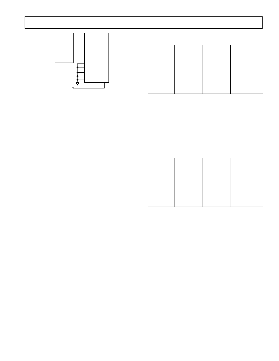
FEATURES
Four 80 MSPS Wideband Inputs (14 Linear Bits Plus 3 RSSI)
4 Real Input Ports/2 Complex Input Ports
Processes 4 Wideband Channels (UMTS or cdma2000
1x) or 8 GSM/EDGE, IS136 Channels
8 Independent Digital Receivers in a Single Package
Four 16-Bit Parallel Output Ports and Four 8-Bit Link Ports
4 Programmable Digital AGC Loops with 96 dB Range
Digital Resampling for Noninteger Decimation Rates
Programmable Decimating FIR Filters
4 Interpolating Half-Band Filters
Flexible Control for Multicarrier and Phased Array
Programmable Attenuator Control for Clip Prevention and
External Gain Ranging via Level Indicator
3.3 V I/O, 2.5 V CMOS Core
User Configurable Built-in Self Test (BIST) Capability
APPLICATIONS
Multicarrier, Multimode Digital Receivers
GSM, IS136, EDGE, PHS, IS95, UMTS, cdma2000
Micro and Pico Cell Systems, Software Radios
Wireless Local Loop
Smart Antenna Systems
In-Building Wireless Telephony

REV. 0
2
AD6635
GENERAL DESCRIPTION
The AD6635 is a multimode, 8-channel, digital Receive Signal
Processor (RSP) capable of processing up to four WCDMA
channels. Each channel consists of four cascaded signal-process-
ing elements: a frequency translator, two CIC decimating filters,
and a programmable coefficient-decimating filter. Each input
port has input level threshold detection circuitry for accommo-
dating large dynamic ranges or situations where gain ranging
converters are used. Quad 16-bit parallel output ports accom-
modate high data rate WBCDMA applications. On-chip
interpolating half-band filters can also be used to further
increase the output rate. In addition, each output port has a
digital AGC for accommodating large dynamic ranges using
smaller bit widths. The AGCs can maintain either signal level or
clipping level, depending on their mode. Link port outputs are
provided to enable glueless interfaces to Analog Devices'
TigerSHARC DSP core.
The AD6635 is part of Analog Devices' SoftCell Multicarrier
transceiver chipset designed for compatibility with Analog Devices'
family of high sample rate IF sampling ADCs (AD9238/AD6645
12-bit and 14-bit). The SoftCell receiver comprises a digital
receiver capable of digitizing an entire spectrum of carriers and
digitally selecting the carrier of interest for tuning and channel
selection. This architecture eliminates redundant radios in wireless
base station applications.
High dynamic range decimation filters offer a wide range of
decimation rates. The RAM-based architecture allows easy
reconfiguration for multimode applications.
The decimating filters remove unwanted signals and noise from
the channel of interest. When the channel of interest occupies
less bandwidth than the input signal, this rejection of out-of-band
noise is called "processing gain." By using large decimation
factors, processing gain can improve the SNR of the ADC by
30 dB or more. In addition, the programmable RAM coefficient
filter allows antialiasing, matched filtering, and static equaliza-
tion functions to be combined in a single, cost-effective filter.
Half-band interpolating filters at the output are used in various
applications, especially in WCDMA or cdma2000 applications,
to increase the output rate from 2
¥ to 4¥ the chip rate. The
AD6635 is equipped with four independent automatic gain
control (AGC) loops for direct interface to a RAKE receiver.
The AD6635 is compatible with standard ADC converters, such
as the AD664x, AD943x, AD923x, and the AD922x families of
data converters. The AD6635 is also compatible with the
AD6600 Diversity ADC, and hence can be designed into exist-
ing systems that use AD6600 ADCs.

REV. 0
AD6635
3
TABLE OF CONTENTS
FEATURES . . . . . . . . . . . . . . . . . . . . . . . . . . . . . . . . . . . . . 1
APPLICATIONS . . . . . . . . . . . . . . . . . . . . . . . . . . . . . . . . . 1
GENERAL DESCRIPTION . . . . . . . . . . . . . . . . . . . . . . . . . 2
ARCHITECTURE . . . . . . . . . . . . . . . . . . . . . . . . . . . . . . . . 5
RECOMMENDED OPERATING CONDITIONS . . . . . . . 7
ELECTRICAL CHARACTERISTICS . . . . . . . . . . . . . . . . . 7
GENERAL TIMING CHARACTERISTICS . . . . . . . . . . . . 8
MICROPROCESSOR PORT TIMING
CHARACTERISTICS . . . . . . . . . . . . . . . . . . . . . . . . . . 10
ABSOLUTE MAXIMUM RATINGS . . . . . . . . . . . . . . . . 11
ORDERING GUIDE . . . . . . . . . . . . . . . . . . . . . . . . . . . . . 11
PIN CONFIGURATION . . . . . . . . . . . . . . . . . . . . . . . . . . 12
PIN CONFIGURATION (PIN OUT) . . . . . . . . . . . . . . . . 13
PIN FUNCTION DESCRIPTION . . . . . . . . . . . . . . . . . . 14
TIMING DIAGRAMS . . . . . . . . . . . . . . . . . . . . . . . . . . . . 16
INPUT DATA PORTS . . . . . . . . . . . . . . . . . . . . . . . . . . . . 23
Input Data Format . . . . . . . . . . . . . . . . . . . . . . . . . . . . . . 23
Input Timing . . . . . . . . . . . . . . . . . . . . . . . . . . . . . . . . . . 23
Input Enable Control . . . . . . . . . . . . . . . . . . . . . . . . . . . . 23
Gain Switching . . . . . . . . . . . . . . . . . . . . . . . . . . . . . . . . . 23
Input Data Scaling . . . . . . . . . . . . . . . . . . . . . . . . . . . . . . 24
Scaling with Fixed-Point ADCs . . . . . . . . . . . . . . . . . . . . 24
Scaling with Floating-Point or Gain-Ranging ADCs . . . . 25
NUMERICALLY CONTROLLED OSCILLATOR . . . . . 26
Frequency Translation . . . . . . . . . . . . . . . . . . . . . . . . . . . 26
NCO Frequency Hold-Off Register . . . . . . . . . . . . . . . . . 26
Phase Offset . . . . . . . . . . . . . . . . . . . . . . . . . . . . . . . . . . . 26
NCO Control Register . . . . . . . . . . . . . . . . . . . . . . . . . . . 26
By-Pass . . . . . . . . . . . . . . . . . . . . . . . . . . . . . . . . . . . . . . 26
Phase Dither . . . . . . . . . . . . . . . . . . . . . . . . . . . . . . . . . . 26
Amplitude Dither . . . . . . . . . . . . . . . . . . . . . . . . . . . . . . . 26
Clear Phase Accumulator on Hop . . . . . . . . . . . . . . . . . . 26
Input Enable Control . . . . . . . . . . . . . . . . . . . . . . . . . . . . 26
Mode 00: Blank on IEN Low . . . . . . . . . . . . . . . . . . . 27
Mode 01: Clock on IEN High . . . . . . . . . . . . . . . . . . . 27
Mode 10: Clock on IEN Transition to High . . . . . . . . 27
Mode 11: Clock on IEN Transition to Low . . . . . . . . . 27
WB Input Select . . . . . . . . . . . . . . . . . . . . . . . . . . . . . . . . 27
Sync Select . . . . . . . . . . . . . . . . . . . . . . . . . . . . . . . . . . . . 27
SECOND-ORDER rCIC FILTER . . . . . . . . . . . . . . . . . . . 27
rCIC2 Rejection . . . . . . . . . . . . . . . . . . . . . . . . . . . . . . . . 28
Example Calculations . . . . . . . . . . . . . . . . . . . . . . . . . . . . 28
Decimation and Interpolation Registers . . . . . . . . . . . . . . 29
rCIC2 Scale . . . . . . . . . . . . . . . . . . . . . . . . . . . . . . . . . . . 29
FIFTH-ORDER CIC FILTER . . . . . . . . . . . . . . . . . . . . . . 29
CIC5 Rejection . . . . . . . . . . . . . . . . . . . . . . . . . . . . . . . . 29
RAM COEFFICIENT FILTER . . . . . . . . . . . . . . . . . . . . . 30
RCF Decimation Register . . . . . . . . . . . . . . . . . . . . . . . . 30
RCF Decimation Phase . . . . . . . . . . . . . . . . . . . . . . . . . . 30
RCF Filter Length . . . . . . . . . . . . . . . . . . . . . . . . . . . . . . 30
RCF Output Scale Factor and Control Register . . . . . . . . 31
INTERPOLATING HALF BAND FILTERS . . . . . . . . . . 32
AUTOMATIC GAIN CONTROL . . . . . . . . . . . . . . . . . . . 32
The AGC Loop . . . . . . . . . . . . . . . . . . . . . . . . . . . . . . . . 33
Desired Signal Level Mode . . . . . . . . . . . . . . . . . . . . . . . 33
Desired Clipping Level Mode . . . . . . . . . . . . . . . . . . . . . 34
Synchronization . . . . . . . . . . . . . . . . . . . . . . . . . . . . . . . . 35
USER CONFIGURABLE BUILT IN SELF TEST
(BIST) . . . . . . . . . . . . . . . . . . . . . . . . . . . . . . . . . . . . . . 35
RAM BIST . . . . . . . . . . . . . . . . . . . . . . . . . . . . . . . . . . . 35
Channel BIST . . . . . . . . . . . . . . . . . . . . . . . . . . . . . . . . . 35
CHIP SYNCHRONIZATION . . . . . . . . . . . . . . . . . . . . . . 36
Start . . . . . . . . . . . . . . . . . . . . . . . . . . . . . . . . . . . . . . . . . 36
Start with No Sync . . . . . . . . . . . . . . . . . . . . . . . . . . . . . . 36
Start with Soft Sync . . . . . . . . . . . . . . . . . . . . . . . . . . . . . 36
Start with Pin Sync . . . . . . . . . . . . . . . . . . . . . . . . . . . . . 36
Hop . . . . . . . . . . . . . . . . . . . . . . . . . . . . . . . . . . . . . . . . . 37
Set Freq No Hop . . . . . . . . . . . . . . . . . . . . . . . . . . . . . . . 37
Hop with Soft Sync . . . . . . . . . . . . . . . . . . . . . . . . . . . . . 37
Hop with Pin Sync . . . . . . . . . . . . . . . . . . . . . . . . . . . . . . 37
PARALLEL OUTPUT PORTS . . . . . . . . . . . . . . . . . . . . . 37
Channel Mode . . . . . . . . . . . . . . . . . . . . . . . . . . . . . . . . . 38
AGC Mode . . . . . . . . . . . . . . . . . . . . . . . . . . . . . . . . . . . 38
Master/Slave PCLKn Modes . . . . . . . . . . . . . . . . . . . . . . 39
Parallel Port Pin Functionality . . . . . . . . . . . . . . . . . . . . . 39
LINK PORT . . . . . . . . . . . . . . . . . . . . . . . . . . . . . . . . . . . . 40
Link Port Data Format . . . . . . . . . . . . . . . . . . . . . . . . . . 40
Link Port Timing . . . . . . . . . . . . . . . . . . . . . . . . . . . . . . . 40
TigerSHARC Configuration . . . . . . . . . . . . . . . . . . . . . . 41
AD6635 CHANNEL MEMORY MAP . . . . . . . . . . . . . . . . 41
0x00-0x7F: Coefficient Memory (CMEM) . . . . . . . . . . . 42
0x80: Channel Sleep Register . . . . . . . . . . . . . . . . . . . . . 42
0x81: Soft_SYNC Register . . . . . . . . . . . . . . . . . . . . . . . 42
0x82: Pin_SYNC Register . . . . . . . . . . . . . . . . . . . . . . . . 42
0x83: Start Hold-Off Counter . . . . . . . . . . . . . . . . . . . . . 42
0x84: NCO Frequency Hold-Off Counter . . . . . . . . . . . 42
0x85: NCO Frequency Register 0 . . . . . . . . . . . . . . . . . . 42
0x86: NCO Frequency Register 1 . . . . . . . . . . . . . . . . . . 42
0x87: NCO Phase Offset Register . . . . . . . . . . . . . . . . . . 42
0x88: NCO Control Register . . . . . . . . . . . . . . . . . . . . . 42
0x90: rCIC2 Decimation 1 (MrCIC2-1) . . . . . . . . . . . 44
0x91: rCIC2 Interpolation 1 (LrCIC2-1) . . . . . . . . . . . 44
0x92: rCIC2 Scale . . . . . . . . . . . . . . . . . . . . . . . . . . . . . 44
0x93: . . . . . . . . . . . . . . . . . . . . . . . . . . . . . . . . . . . . . . . . 44
0x94: CIC5 Decimation 1 (MCIC5-1) . . . . . . . . . . . . . 44
0x95: CIC5 Scale . . . . . . . . . . . . . . . . . . . . . . . . . . . . . . 44
0x96: . . . . . . . . . . . . . . . . . . . . . . . . . . . . . . . . . . . . . . . . 44
0xA0: RCF Decimation 1 (MRCF-1) . . . . . . . . . . . . . 44
0xA1: RCF Decimation Phase (PRCF) . . . . . . . . . . . . . . 44
0xA2: RCF Number of Taps Minus 1 (NRCF-1) . . . . . . 44
0xA3: RCF Coefficient Offset (CORCF) . . . . . . . . . . . . 44
0xA4: RCF Control Register . . . . . . . . . . . . . . . . . . . . . . 45
0xA5: BIST Register for I . . . . . . . . . . . . . . . . . . . . . . . . 45
0xA6: BIST Register for Q . . . . . . . . . . . . . . . . . . . . . . . 45
0xA7: BIST Control Register . . . . . . . . . . . . . . . . . . . . . 45
0xA8: RAM BIST Control Register . . . . . . . . . . . . . . . . 45
0xA9: Output Control Register . . . . . . . . . . . . . . . . . . . . 45
Memory Map for Input Port Control Registers . . . . . . . . . . 46
Input Port Control Registers . . . . . . . . . . . . . . . . . . . . . . . . 46
0x00: Lower Threshold A: . . . . . . . . . . . . . . . . . . . . . . . . 46
0x01: Upper Threshold A: . . . . . . . . . . . . . . . . . . . . . . . . 46
0x02: Dwell Time A: . . . . . . . . . . . . . . . . . . . . . . . . . . . . 46
0x03: Gain Range A Control Register: . . . . . . . . . . . . . . . 46
0x04: Lower Threshold B: . . . . . . . . . . . . . . . . . . . . . . . . 47
0x05: Upper Threshold B: . . . . . . . . . . . . . . . . . . . . . . . . 47
0x06: Dwell Time B: . . . . . . . . . . . . . . . . . . . . . . . . . . . . 47
0x07: Gain Range B Control Register: . . . . . . . . . . . . . . . 47
Memory Map for Output Port Control Registers . . . . . . . . . 47

REV. 0
4
AD6635
0x08: Port A Control Register . . . . . . . . . . . . . . . . . . . . . 50
0x09: Port B Control Register . . . . . . . . . . . . . . . . . . . . . 50
0x0A AGC A Control Register . . . . . . . . . . . . . . . . . . . . . 50
0x0B AGC A Hold off Counter . . . . . . . . . . . . . . . . . . . . 50
0x0C AGC A Desired Level . . . . . . . . . . . . . . . . . . . . . . . 50
0x0D AGC A Signal Gain . . . . . . . . . . . . . . . . . . . . . . . . 51
0x0E AGC A Loop Gain . . . . . . . . . . . . . . . . . . . . . . . . . 51
0x0F AGC A Pole Location . . . . . . . . . . . . . . . . . . . . . . . 51
0x10 AGC A Average Samples . . . . . . . . . . . . . . . . . . . . . 51
0x11 AGC A Update Decimation . . . . . . . . . . . . . . . . . . 51
0x12 AGC B Control Register . . . . . . . . . . . . . . . . . . . . . 51
0x13 AGC B Hold off Counter . . . . . . . . . . . . . . . . . . . . 51
0x14 AGC B Desired Level . . . . . . . . . . . . . . . . . . . . . . . 51
0x15 AGC B Signal Gain . . . . . . . . . . . . . . . . . . . . . . . . . 51
0x16 AGC B Loop Gain . . . . . . . . . . . . . . . . . . . . . . . . . 51
0x17 AGC B Pole Location . . . . . . . . . . . . . . . . . . . . . . . 52
0x18 AGC B Average Samples . . . . . . . . . . . . . . . . . . . . . 52
0x19 AGC B Update Decimation . . . . . . . . . . . . . . . . . . 52
0x1A Parallel Port Control A . . . . . . . . . . . . . . . . . . . . . . 52
0x1B Link Port Control A . . . . . . . . . . . . . . . . . . . . . . . . 52
0x1C Parallel Port Control B . . . . . . . . . . . . . . . . . . . . . . 52
0x1D Link Port Control B . . . . . . . . . . . . . . . . . . . . . . . . 53
0x1E Port Clock Control . . . . . . . . . . . . . . . . . . . . . . . . . 53
TABLE OF CONTENTS
MICROPORT CONTROL . . . . . . . . . . . . . . . . . . . . . . . . 53
External Memory Map . . . . . . . . . . . . . . . . . . . . . . . . . . . 53
Access Control Register (ACR) . . . . . . . . . . . . . . . . . . . . 54
Channel Address Register (CAR) . . . . . . . . . . . . . . . . . . . 54
SOFT_SYNC Control Register . . . . . . . . . . . . . . . . . . . . 55
PIN_SYNC Control Register . . . . . . . . . . . . . . . . . . . . . . 55
SLEEP Control Register . . . . . . . . . . . . . . . . . . . . . . . . . 55
Data Address Registers . . . . . . . . . . . . . . . . . . . . . . . . . . 55
Write Sequencing . . . . . . . . . . . . . . . . . . . . . . . . . . . . . . . 55
Read Sequencing . . . . . . . . . . . . . . . . . . . . . . . . . . . . . . . 55
Read/Write Chaining . . . . . . . . . . . . . . . . . . . . . . . . . . . . 56
Intel Nonmultiplexed Mode (INM) . . . . . . . . . . . . . . . . . 56
Motorola Nonmultiplexed Mode (MNM) . . . . . . . . . . . . 56
SERIAL PORT CONTROL . . . . . . . . . . . . . . . . . . . . . . . . 56
Serial Port Timing Specifications . . . . . . . . . . . . . . . . . . . 56
SDI0, SDI4 . . . . . . . . . . . . . . . . . . . . . . . . . . . . . . . . . . . 56
SCLK0, SCLK4 . . . . . . . . . . . . . . . . . . . . . . . . . . . . . . . 56
INTERNAL WRITE ACCESS . . . . . . . . . . . . . . . . . . . . . . 58
Write Pseudocode . . . . . . . . . . . . . . . . . . . . . . . . . . . . . . 58
INTERNAL READ ACCESS . . . . . . . . . . . . . . . . . . . . . . . 58
Read Pseudocode . . . . . . . . . . . . . . . . . . . . . . . . . . . . . . . 58
OUTLINE DIMENSIONS . . . . . . . . . . . . . . . . . . . . . . . . . 59

REV. 0
AD6635
5
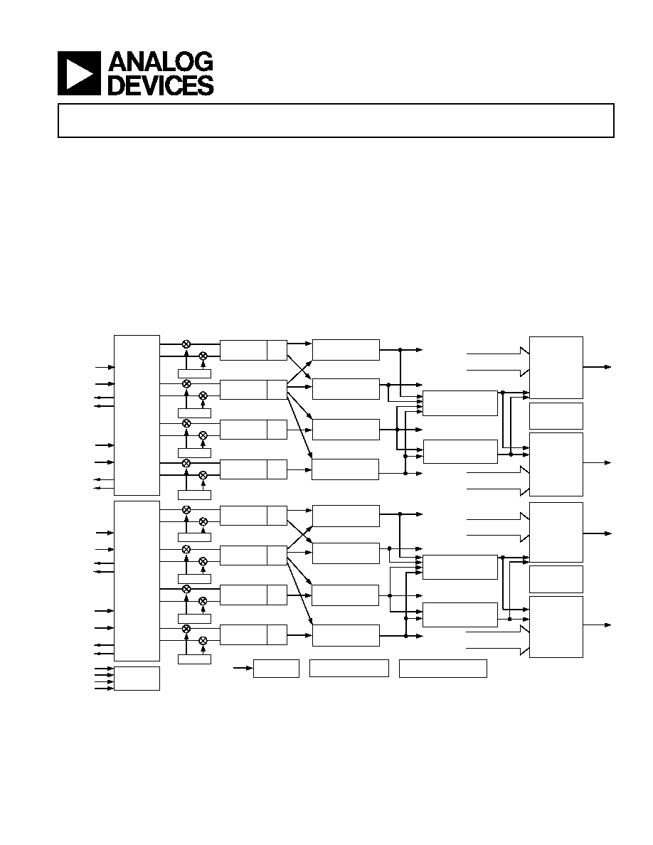
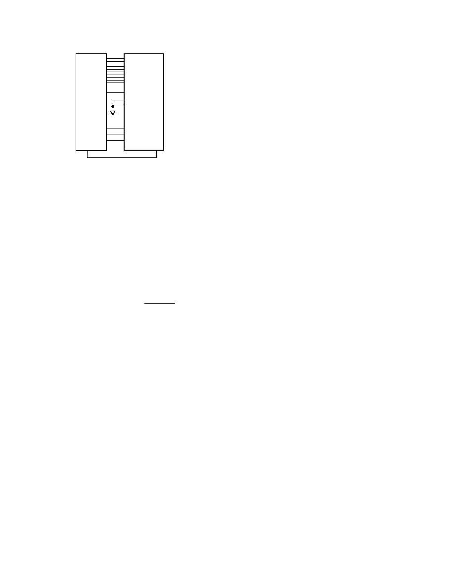
ARCHITECTURE
Each channel of the AD6635 has four signal processing stages:
a Frequency Translator, a second-order Resampling Cascaded
Integrator Comb FIR Filter (rCIC2), a fifth-order Cascaded
Integrator Comb FIR Filter (CIC5), and a RAM Coefficient
FIR Filter (RCF). Multiple modes are supported for clocking
data into and out of the chip, and for providing flexibility for inter-
facing to a wide variety of digitizers. Programming and control is
accomplished via serial and/or microprocessor interfaces.
Frequency translation is accomplished with a 32-bit complex
Numerically Controlled Oscillator (NCO). Real data entering
this stage is separated into inphase (I) and quadrature (Q) com-
ponents by multiplying with the complex NCO word. This stage
translates the input signal from a digital intermediate frequency
(IF) to digital baseband. Phase and amplitude dither may be
enabled on-chip to improve spurious performance of the NCO.
A phase-offset word is available to create a known phase rela-
tionship between multiple AD6635s or between channels.
Following frequency translation is a fixed coefficient, high speed,
second-order, Resampling Cascade Integrator Comb (rCIC2) filter
that reduces the sample rate based on the ratio between the deci-
mation and interpolation registers.
The next stage is a fifth-order Cascaded Integrator Comb (CIC5)
filter whose response is defined by the decimation rate. The pur-
pose of these filters is to reduce the data rate to the final filter stage
(RCF), so that it can calculate more taps for the same RCF band-
width. The CIC5 filter has better antialiasing (filtering) compared
to rCIC2. In light of this, the user is advised to use this filter only if
resampling is required or if the required decimation cannot be
handled by CIC5 alone.
The final stage is a sum-of-products FIR filter with program-
mable 20-bit coefficients, and decimation rates programmable
from 1 to 256 (1 to 32 in practice). The RAM Coefficient FIR
Filter (RCF) can handle a maximum of 160 taps.
The data coming out of the RCF can be sent to output ports or
to an interleaver. This section can interleave data from more
than one channel. One carrier can be processed using more than
one channel and the interleaver will interleave the data back into
the output section. This way, processing power from more than
one channel can be used for one carrier.
The interleaved data is sent into a fixed coefficient half-band
interpolation filter where data is interpolated by a factor of two.
Digital AGC following the half-band filter has a gain range of
96.3 dB. This AGC section is completely programmable in
terms of its response. Four each of half-band filters and AGCs
are present in the AD6635, as shown in the Functional Block
Diagram. These half-band filters and AGC sections can be
bypassed independent of each other.
The overall filter response for the AD6635 is the composite of
all decimating and interpolating stages. Each successive filter
stage is capable of narrower transition bandwidths, but requires
a greater number of CLK cycles to calculate the output. More
decimation in the first filter stage will minimize overall power
consumption. Each independent filter stage can be bypassed in
a unique way. Data from the chip is interfaced to the DSP via
either a high speed parallel port or a TigerSHARC compatible
link port. Each output can be independently configured to use
either the parallel port or the link port.
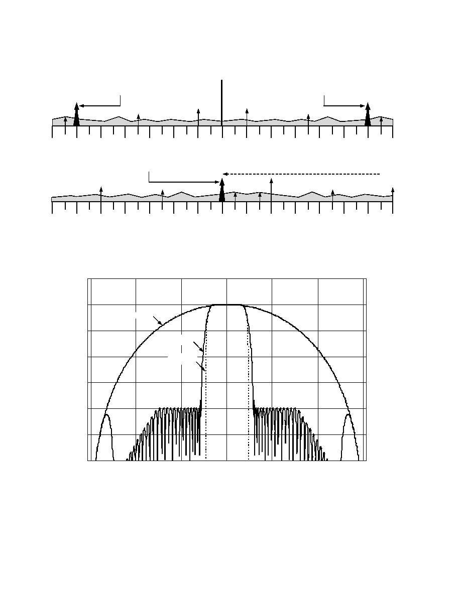
Figure 1 illustrates the tuning function of the AD6635 NCOs to
select and filter a single channel from a wide input spectrum.
The frequency translator "tunes" the desired carrier to base-
band. Figure 2 shows the combined filter response of the rCIC2,
CIC5, and RCF filters for a sample filter configuration.
REV. 0
6
AD6635
f
S
/2
3
f
S
/8
5
f
S
/16
f
S
/4
3
f
S
/16
f
S
/8
f
S
/16
dc
f
S
/16
f
S
/8
3f
S
/16
f
S
/4
5f
S
/16
3f
S
/8
f
S
/2
FREQUENCY TRANSLATION (e.g., SINGLE 1MHz CHANNEL TUNED TO BASEBAND)
AFTER FREQUENCY TRANSLATION
NCO "TUNES" SIGNAL TO BASEBAND
f
S
/2
3
f
S
/8
5
f
S
/16
f
S
/4
3
f
S
/16
f
S
/8
f
S
/16
dc
f
S
/16
f
S
/8
3f
S
/16
f
S
/4
5f
S
/16
3f
S
/8
f
S
/2
SIGNAL OF INTEREST "IMAGE"
SIGNAL OF INTEREST
WIDEBAND INPUT SPECTRUM
(
f
SAMPLE
/2 TO
f
SAMPLE
/2)
WIDEBAND INPUT SPECTRUM (e.g., 30MHz FROM HIGH SPEED ADC)
Figure 1. AD6635 Frequency Translation of Wideband Input Spectrum
1.5
10
4
kHz
20
dBc
0
20
40
60
80
100
120
1.0
10
4
5000
0
5000
1.0
10
4
1.5
10
4
CIC RESPONSE
COMPOSITE
RESPONSE
DESIRED
RESPONSE
Figure 2. Composite Filter Response of rCIC2, CIC5, and RCF for a Sample Filter Configuration

REV. 0
AD6635
7
Test
AD6635BB
Parameter
Temp
Level
Min
Typ
Max
Unit
VDD
IV
2.25
2.5
2.75
V
VDDIO
IV
3.0
3.3
3.6
V
T
AMBIENT
IV
40
+25
+85
C
RECOMMENDED OPERATING CONDITIONS
Test
AD6635BB
Parameter (Conditions)
Temp
Level
Min
Typ
Max
Unit
LOGIC INPUTS (5 V TOLERANT)
Logic Compatibility
Full
IV
3.3 V CMOS
Logic 1 Voltage
Full
IV
2.0
5.0
V
Logic 0 Voltage
Full
IV
0.3
+0.8
V
Logic 1 Current
Full
IV
1
10
A
Logic 0 Current
Full
IV
1
10
A
Logic 1 Current (inputs with pull-down)
Full
IV
Logic 0 Current (inputs with pull-up)
Full
IV
Input Capacitance
25
C
V
4
pF
LOGIC OUTPUTS
Logic Compatibility
Full
IV
Logic 1 Voltage (I
OH
= 0.25 mA)
Full
IV
2.4
VDD 0.2
V
Logic 0 Voltage (I
OL
= 0.25 mA)
Full
IV
0.2
0.4
V
IDD SUPPLY CURRENT
CLK = 80 MHz, (VDD = 2.75 V, VDDIO = 3.6 V)
Full
IV
I
VDD
880
mA
I
VDDIO
150
mA
CLK = GSM Example (65 MSPS, VDD = 2.5 V,
VDDIO = 3.3 V, 4 Channels)
25
C
V
I
VDD
485
mA
I
VDDIO
60
mA
CLK = WCDMA Example (76.8 MSPS,
VDD = 2.5V, VDDIO = 3.3 V, 2 Channels)
25
C
V
I
VDD
830
mA
I
VDDIO
120
mA
POWER DISSIPATION
CLK = 80 MHz
Full
IV
2.8
W
CLK = 65 MHz GSM/EDGE Example
V
1.4
mW
CLK = 76.8 MHz WCDMA Example
V
2.5
W
CLK = 78.64 MHz cdma2000 Example
V
2.3
W
All Channels in Sleep Mode
Full
IV
570
W
Specifications subject to change without notice.
ELECTRICAL CHARACTERISTICS
SPECIFICATIONS

REV. 0
8
AD6635
SPECIFICATIONS
(continued)
GENERAL TIMING CHARACTERISTICS
1, 2
Test
AD6635BB
Parameter (Conditions)
Temp
Level
Min
Typ
Max
Unit
CLKn TIMING REQUIREMENTS
t
CLK
CLKn Period
Full
I
12.5
ns
t
CLKL
CLKn Width Low
Full
IV
5.6
0.5 t
CLK
ns
t
CLKH
CLKn Width High
Full
IV
5.6
0.5 t
CLK
ns
RESET TIMING REQUIREMENTS
t
RESL
RESET Width Low
Full
I
30.0
ns
INPUT WIDEBAND DATA TIMING REQUIREMENTS
t
SI
Input to
CLKn Setup Time
Full
IV
2.0
ns
t
HI
Input to
CLKn Hold Time
Full
IV
1.0
ns
LEVEL INDICATOR OUTPUT SWITCHING CHARACTERISTICS
t
DLI
CLKn to LIx-y Output Delay Time
Full
IV
3.3
10.0
ns
SYNC TIMING REQUIREMENTS
t
SS
SYNC(A, B, C, D) to
CLKn Setup Time
Full
IV
2.0
ns
t
HS
SYNC(A, B, C, D) to
CLKn Hold Time
Full
IV
1.0
ns
SERIAL PORT CONTROL TIMING REQUIREMENTS
SWITCHING CHARACTERISTICS
2
t
SCLK
SCLKn (n = 0, 4) Period
Full
IV
16
ns
t
SCLKL
SCLKn Low Time
Full
IV
3.0
ns
t
SCLKH
SCLKn High Time
Full
IV
3.0
ns
INPUT CHARACTERISTICS
t
SSI
SDIn to
ØSCLKn Setup Time
Full
IV
1.0
ns
t
HSI
SDIn to
ØSCLKn Hold Time
Full
IV
1.0
ns
PARALLEL PORT TIMING REQUIREMENTS
(MASTER MODE) SWITCHING CHARACTERISTICS
3
t
DPOCLKL
ØCLKn to PCLKn Delay (Divide by 1)
Full
IV
6.5
10.5
ns
t
DPOCLKLL
ØCLKn to PCLKn Delay (Divide by 2, 4, or 8) Full
IV
8.3
14.6
ns
t
DPREQ
CLKn to PxREQ Delay
1.0
ns
t
DPP
CLKn to Px[15:0] Delay
0.0
ns
INPUT CHARACTERISTICS
t
SPA
PxACK to
ØPCLKn Setup Time
7.0
ns
t
HPA
PxACK to
ØPCLKn Hold Time
3.0
ns
PARALLEL PORT TIMING REQUIREMENTS
(SLAVE MODE) SWITCHING CHARACTERISTICS
3
t
POCLK
PCLKn Period
Full
I
12.5
ns
t
POCLKL
PCLKn Low Period (when PCLK Divisor = 1)
Full
IV
2.0
0.5 t
POCLK
ns
t
POCLKH
PCLKn High Period (when PCLK Divisor = 1)
Full
IV
2.0
0.5 t
POCLK
ns
t
DPREQ
CLKn to PxREQ Delay
10.0
ns
t
DPP
CLKn to Px[15:0] Delay
11.0
ns

REV. 0
AD6635
9
GENERAL TIMING CHARACTERISTICS
1, 2
Test
AD6635BB
Parameter (Conditions)
Temp
Level
Min
Typ
Max
Unit
INPUT CHARACTERISTICS
t
SPA
PxACK to
ØPCLKn Setup Time
1.0
ns
t
HPA
PxACK to
ØPCLKn Hold Time
1.0
ns
LINK PORT TIMING REQUIREMENTS
SWITCHING CHARACTERISTICS
3
t
RDLCLK
PCLKn to LxCLKOUT Delay
Full
IV
2.5
ns
t
FDLCLK
ØPCLKn to ØLxCLKOUT Delay
Full
IV
0
ns
t
RLCLKDAT
LxCLKOUT to Lx[7:0] Delay
Full
IV
0
2.9
ns
t
FLCLKDAT
ØLxCLKOUT to Lx[7:0] Delay
Full
IV
0
2.2
ns
NOTES
1
All Timing Specifications valid over VDD range of 2.25 V to 2.75 V, and VDDIO range of 3.0 V to 3.6 V.
2
C
LOAD
= 40 pF on all outputs unless otherwise specified.
3
The timing parameters for Px[15:0], PxREQ, PxACK, LxCLKOUT, and Lx[7:0] apply for output ports A, B, C, and D. (x stands for A, B, C, or D.)
Specifications subject to change without notice.

REV. 0
10
AD6635
MICROPROCESSOR PORT TIMING CHARACTERISTICS
1, 2
Test
AD6635BB
Parameter (Conditions)
Temp
Level
Min
Typ
Max
Unit
MICROPROCESSOR PORT, MODE MNM (MODE = 0)
MODE INM WRITE TIMING
t
SC
Control
3
to
CLKn Setup Time
Full
IV
2.0
ns
t
HC
Control
3
to
CLKn Hold Time
Full
IV
2.5
ns
t
HWR
WR(RW) to RDY(DTACK) Hold Time
Full
IV
7.0
ns
t
SAM
Address/Data to
WR(RW) Setup Time
Full
IV
3.0
ns
t
HAM
Address/Data to RDY(
DTACK) Hold Time
Full
IV
5.0
ns
t
DRDY
WR(RW) to RDY(DTACK) Delay
Full
IV
8.0
ns
t
ACC
WR(RW) to RDY(DTACK) High Delay
Full
IV
4 t
CLK
5 t
CLK
9 t
CLK
ns
MODE INM READ TIMING
t
SC
Control
3
to
CLKn Setup Time
Full
IV
5.0
ns
t
HC
Control
3
to
CLKn Hold Time
Full
IV
2.0
ns
t
SAM
Address to
RD(DS) Setup Time
Full
IV
0.0
ns
t
HAM
Address to Data Hold Time
Full
IV
5.0
ns
t
DRDY
RD(DS) to RDY(DTACK) Delay
Full
IV
8.0
ns
t
ACC
RD(DS) to RDY(DTACK) High Delay
Full
IV
8 t
CLK
10 t
CLK
13 t
CLK
ns
MICROPROCESSOR PORT, MODE MNM (MODE = 1)
MODE MNM WRITE TIMING
t
SC
Control
3
to
CLKn Setup Time
Full
IV
2.0
ns
t
HC
Control
3
to
CLKn Hold Time
Full
IV
2.5
ns
t
HDS
DS(RD) to DTACK(RDY) Hold Time
Full
IV
8.0
ns
t
HRW
RW(
WR) to DTACK(RDY) Hold Time
Full
IV
7.0
ns
t
SAM
Address/Data to RW(
WR) Setup Time
Full
IV
3.0
ns
t
HAM
Address/Data to RW(
WR) Hold Time
Full
IV
5.0
ns
t
DDTACK
DS(RD) to DTACK(RDY) Delay
Full
IV
8.0
ns
t
ACC
RW(
WR) to DTACK(RDY) Low Delay
Full
IV
4 t
CLK
5 t
CLK
9 t
CLK
ns
MODE MNM READ TIMING
t
SC
Control
3
to
CLKn Setup Time
Full
IV
5.0
ns
t
HC
Control
3
to
CLKn Hold Time
Full
IV
2.0
ns
t
HDS
DS(RD) to DTACK(RDY) Hold Time
Full
IV
8.0
ns
t
SAM
Address to
DS(RD) Setup Time
Full
IV
0.0
ns
t
HAM
Address to Data Hold Time
Full
IV
5.0
ns
t
DDTACK
DS(RD) to DTACK(RDY) Delay
Full
IV
8.0
ns
t
ACC
DS(RD) to DTACK(RDY) Low Delay
Full
IV
8 t
CLK
10 t
CLK
13 t
CLK
ns
NOTES
1
All Timing Specifications valid over VDD range of 2.25 V to 2.75 V, and VDDIO range of 3.0 V to 3.6 V.
2
C
LOAD
= 40 pF on all outputs unless otherwise specified.
3
Specification pertains to control signals: R/W, (
WR), DS, (RD), CS0, CS1.
Specifications subject to change without notice.

REV. 0
AD6635
11
CAUTION
ESD (electrostatic discharge) sensitive device. Electrostatic charges as high as 4000 V readily
accumulate on the human body and test equipment and can discharge without detection. Although the
AD6635 features proprietary ESD protection circuitry, permanent damage may occur on devices
subjected to high energy electrostatic discharges. Therefore, proper ESD precautions are recommended
to avoid performance degradation or loss of functionality.
ABSOLUTE MAXIMUM RATINGS
*
Supply Voltage . . . . . . . . . . . . . . . . . . . . . . . . . . . . . . . . . 3.6 V
Input Voltage . . . . . . . . . . . . . 0.3 V to +5.3 V (5 V Tolerant)
Output Voltage Swing . . . . . . . . . . . 0.3 V to VDDIO + 0.3 V
Load Capacitance . . . . . . . . . . . . . . . . . . . . . . . . . . . . . 200 pF
Junction Temperature Under Bias . . . . . . . . . . . . . . . . . 150
C
Storage Temperature Range . . . . . . . . . . . . . 65
C to +150C
Lead Temperature (5 sec) . . . . . . . . . . . . . . . . . . . . . . . 280
C
*Stresses greater than those listed above may cause permanent damage to the device
These are stress ratings only; functional operation of the devices at these or any
other conditions greater than those indicated in the operational sections of this
specification is not implied. Exposure to absolute maximum rating conditions for
extended periods may affect device reliability.
Thermal Characteristics
324-Lead BGA:
JA
= 16.87
C/W, no airflow.
Thermal measurements made in the horizontal position on a
4-layer board.
EXPLANATION OF TEST LEVELS
I
100% Production Tested.
II
100% Production Tested at 25
C, and Sample Tested at
Specified Temperatures.
III
Sample Tested Only.
IV
Parameter Guaranteed by Design and Analysis.
V
Parameter is Typical Value Only.
VI
100% Production Tested at 25
C, and Sample Tested at
Temperature Extremes.
ORDERING GUIDE
Model
Temperature Range
Package Descriptions
Package Option
AD6635BB
40ºC to +85ºC
324-Lead PBGA (Ball Grid Array)
B-324
AD6635BB/PCB
Evaluation Board with AD6635 and Software
REV. 0
12
AD6635
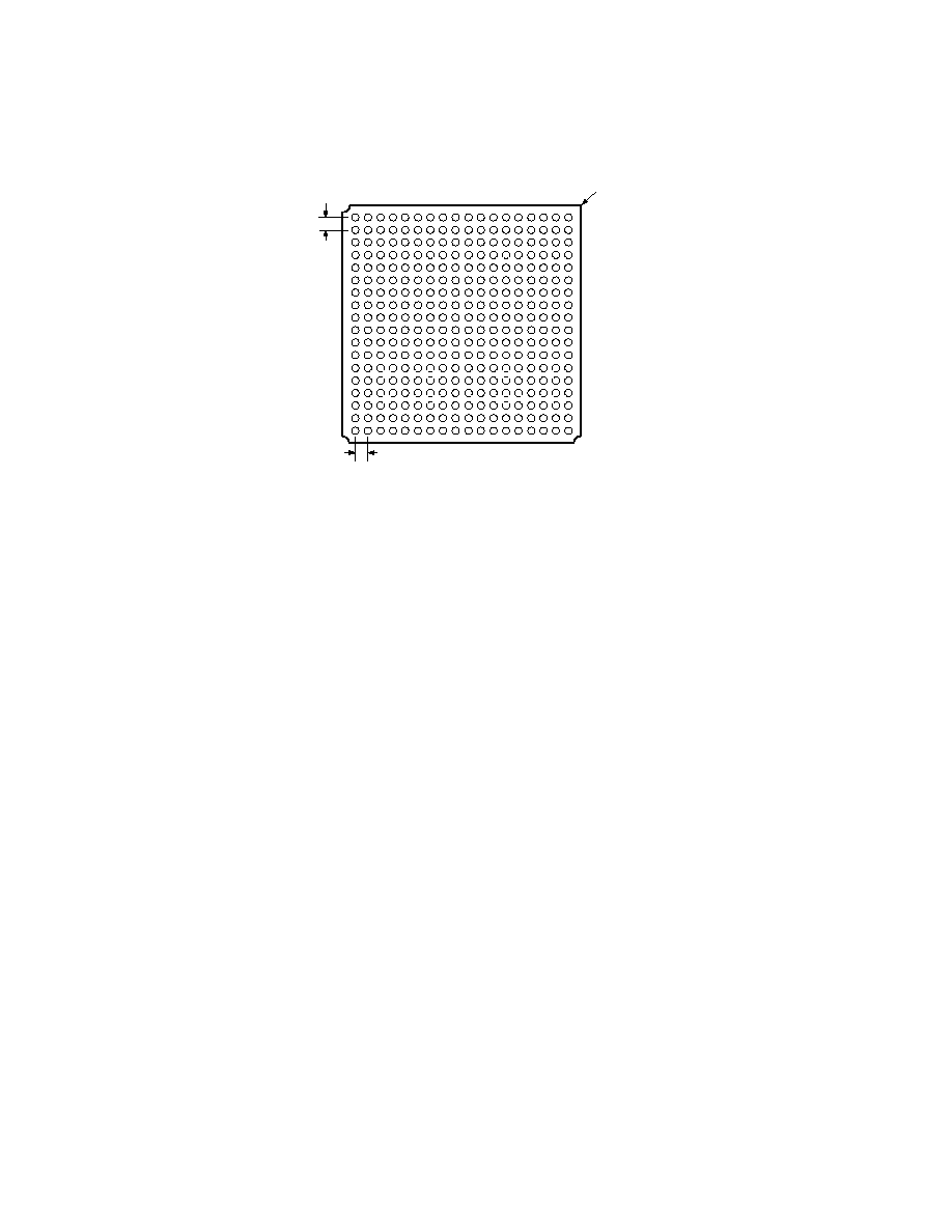
PIN CONFIGURATION
19mm 19mm 18
2
BALL ZAPHOD PACKAGE
1.00
BSC
1.00
BSC
BOTTOM VIEW
A
B
C
D
E
F
G
H
J
K
L
M
N
P
R
T
U
V
1
2
3
4
5
6
7
8
9
10
18 17 16 15 14 13 12 11
A1 BALL
CORNER

REV. 0
AD6635
13
PIN CONFIGURATION (PIN OUT)
1
2
3
4
5
6
7
8
9
10
11
12
13
14
15
16
17
18
A
IENC
INC0
INC7
INC12
IND2
IND3
IND7
IND8
IND11
EXPD1
PDREQ
PD14
PD10
PD8
PD5_LD5
PDCH1_
LDCLK
IN
A
B
CLK0
VDDIO
(Reserved)
INC1
INC8
INC11
IND1
IND4
IND6
IND9
IND12
EXPD2
PDACK
PD12
PD11
PD4_LD4
PD3_LD3
PD7_LD7
PDCH0_
LDCLK
OUT
B
C
CLK1
PAREQ
INC2
INC9
LID-B
IND0
IND5
IND10
IND13
EXPD0
PD15
PD9
PD1_LD1
PD2_LD2
PD0_LD0
SDI4
PDIQ
C
D
PAACK
CHIP0_ID0
LID-A
INC3
INC10
INC13
IEND
EXPC0
VDD
VDD
VDD
PD13
PCACK
CHIP1_ID1
PCIQ
PD6_LD6
PCLK1
D
E
CHIP0_ID1 CHIP0_ID2
INC4
INC5
INC6
EXPC2
EXPC1
VDD
VDD
VDD
VDDIO
(Reserved)
DNC
CHIP1_ID0 CHIP1_ID2
SCLK4
E
F
SCLK0
PAIQ
VDD
VDD
VDD
VDDIO
VDDIO
VDDIO
GND
GND
GND
VDDIO
VDDIO
VDDIO
PCREQ
PC14
PC15
F
G
PCLK0
SDI0
PB6_LB6
VDD
VDD
VDD
VDDIO
VDDIO
VDDIO
GND
GND
GND
VDDIO
VDDIO
VDDIO
PC11
PC13
PC12
G
H
PBCH0_
LBCLK
OUT
PBIQ
PB7_LB7
GND
GND
GND
GND
GND
GND
GND
GND
GND
GND
GND
GND
PC10
PC9
DNC
H
J
PBCH1_
LBCLK
IN
PB0_LB0
PB3_LB3
GND
GND
GND
GND
GND
GND
GND
GND
GND
GND
GND
GND
PC8
PC0_LC0
GND
(Reserved)
J
K
PB2_LB2
PB4_LB4
PB5_LB5
GND
GND
GND
GND
GND
GND
GND
GND
GND
GND
GND
GND
PC1_LC1
PC3_LC3
PC2_LC2
K
L
PB11
PB1_LB1
PB8
GND
GND
GND
GND
GND
GND
GND
GND
GND
GND
GND
GND
A1
PC5_LC5
PC4_LC4
L
M
PB13
PB9
PB10
VDDIO
VDDIO
VDDIO
VDD
VDD
VDD
VDDIO
VDDIO
VDDIO
VDD
VDD
VDD
PC6_LC6
PC7_L
C7
PCCH1_
LCCLK
IN
M
N
PB12
PB14
VDDIO
VDDIO
VDDIO
VDD
VDD
VDD
VDDIO
VDDIO
VDDIO
VDD
VDD
VDD
A0
A2
PCCH0_
LCCLK
OUT
N
P
PBREQ
PB15
PBACK
PA15
PA14
PA13
PA10
PA12
PA11
PA3_LA3
LIC-A
DNC
DNC
DNC
D7
D0
D1
DS
P
R
EXPB0
INB10
INB11
INB12
INB13
EXPA0
EXPA2
PA9
PA8
LIC-B
PA5_LA5
CS0
DNC
D4
D3
CS1
R/W
R
T
EXPB1
INB9
INB4
INB3
INB0
EXPA1
INA9
INA8
PA0_LA0
PA2_LA2
PA1_LA1
SYNCD
DTACK
RESET
PA7_LA7
DNC
D5
D2
T
U
EXPB2
INB8
INB5
INB2
LIB-B
INA13
INA10
INA7
INA5
INA3
INA1
LIA-A
SYNCA
SYNCC
PA6_LA6
PA4_LA4
MODE
D6
U
V
INB7
INB6
INB1
IENB
INA12
INA11
INA6
INA4
INA2
INA0
IENA
LIB-A
LIA-B
SYNCB
PACH0_
LACLK
OUT
PACH1_
LACLK
IN
V
1
2
3
4
5
6
7
8
9
10
11
12
13
14
15
16
17
18
VDDIO
(Reserved)
VDDIO
(Reserved)
VDDIO
(Reserved)

REV. 0
14
AD6635
PIN FUNCTION DESCRIPTION
Name
Type
Function
POWER SUPPLY
VDD
P
2.5 V Core Supply (also called DVCORE)
VDDIO
P
3.3 V IO Supply (also called DVRING)
GND
G
Ground
INPUTS
INA[13:0]
1
I
A Input Data (Mantissa)
EXPA[2:0]
1
I
A Input Data (Exponent)
IENA
2
I
Input Enable--Input A
INB[13:0]
1
I
B Input Data (Mantissa)
EXPB[2:0]
1
I
B Input Data (Exponent)
IENB
2
I
Input Enable--Input B
INC[13:0]
1
I
C Input Data (Mantissa)
EXPC[2:0]
1
I
C Input Data (Exponent)
IENC
2
I
Input Enable--Input C
IND[13:0]
1
I
D Input Data (Mantissa)
EXPD[2:0]
1
I
D Input Data (Exponent)
IEND
2
I
Input Enable--Input D
RESET
I
Active Low Reset Pin
CLK0
I
Input Clock 0 (Master Clock for Channels 03 and Ports A, B)
CLK1
I
Input Clock 1 (Master Clock for Channels 47 and Ports C, D)
PCLK0
I/O
Link/Parallel Port Clock for Output Ports A and B
PCLK1
I/O
Link/Parallel Port Clock for Output Ports C and D
LACLKIN
I
Link Port A Data Ready
LBCLKIN
I
Link Port B Data Ready
LCCLKIN
I
Link Port C Data Ready
LDCLKIN
I
Link Port D Data Ready
SYNCA
1
I
All Sync Pins Go to All Eight Channels
SYNCB
1
I
All Sync Pins Go to All Eight Channels
SYNCC
1
I
All Sync Pins Go to All Eight Channels
SYNCD
1
I
All Sync Pins Go to All Eight Channels
CHIP0_ID[2:0]
1
I
Chip ID Selector for Channels 03 and Ports A, B
CHIP1_ID[2:0]
1
I
Chip ID Selector for Channels 47 and Ports C, D
CONTROL
PAACK
I
Parallel Port A Acknowledge
PAREQ
O
Parallel Port A Request
PBACK
I
Parallel Port B Acknowledge
PBREQ
O
Parallel Port B Request
PCACK
I
Parallel Port C Acknowledge
PCREQ
O
Parallel Port C Request
PDACK
I
Parallel Port D Acknowledge
PDREQ
O
Parallel Port D Request

REV. 0
AD6635
15
PIN FUNCTION DESCRIPTION (continued)
Name
Type
Function
MICROPORT CONTROL
D[7:0]
I/O/T
Bidirectional Microport Data
A[2:0]
I
Microport Address Bus
DS (RD)
I
Active Low Data Strobe (Active Low Read)
DTACK (RDY)
2
O/T
Active Low Data Acknowledge (Microport Status Bit)
R/W (
WR)
I
Read Write (Active Low Write)
MODE
I
Intel or Motorola Mode Select
CS0
1
I
Chip Select for Channels 03 and Ports A, B
CS1
1
I
Chip Select for Channels 47 and Ports C, D
SERIAL PORT CONTROL
SDI0
1
I
Serial Port Control Data Input for Channels 03 and Ports A, B
SCLK0
1
I
Serial Port Control Clock for Channels 03 and Ports A, B
SDI4
1
I
Serial Port Control Data Input for Channels 47 and Ports C, D
SCLK4
1
I
Serial Port Control Clock for Channels 47 and Ports C, D
OUTPUTS
LIA-A
O
Level Indicator--Input A, Interleaved-Data A
LIA-B
O
Level Indicator--Input A, Interleaved-Data B
LIB-A
O
Level Indicator--Input B, Interleaved-Data A
LIB-B
O
Level Indicator--Input B, Interleaved-Data B
LIC-A
O
Level Indicator--Input C, Interleaved-Data A
LIC-B
O
Level Indicator--Input C, Interleaved-Data B
LID-A
O
Level Indicator--Input D, Interleaved-Data A
LID-B
O
Level Indicator--Input D, Interleaved-Data B
LACLKOUT
O
Link Port A Clock Output
LBCLKOUT
O
Link Port B Clock Output
LCCLKOUT
O
Link Port C Clock Output
LDCLKOUT
O
Link Port D Clock Output
LA[7:0]
O
Link Port A Output Data
LB[7:0]
O
Link Port B Output Data
LC[7:0]
O
Link Port C Output Data
LD[7:0]
O
Link Port D Output Data
PA[15:0]
O
Parallel Output Data Port A
PB[15:0]
O
Parallel Output Data Port B
PC[15:0]
O
Parallel Output Data Port C
PD[15:0]
O
Parallel Output Data Port D
PACH[1:0]
O
Parallel Output Port A Channel Indicator
PBCH[1:0]
O
Parallel Output Port B Channel Indicator
PCCH[1:0]
O
Parallel Output Port C Channel Indicator
PDCH[1:0]
O
Parallel Output Port D Channel Indicator
PAIQ
O
Parallel Port A I/Q Data Indicator
PBIQ
O
Parallel Port B I/Q Data Indicator
PCIQ
O
Parallel Port C I/Q Data Indicator
PDIQ
O
Parallel Port D I/Q Data Indicator
NOTES
1
Pins with a pull-down resistor of nominal 70 k
W.
2
Pins with a pull-up resistor of nominal 70 k
W.
REV. 0
16
AD6635
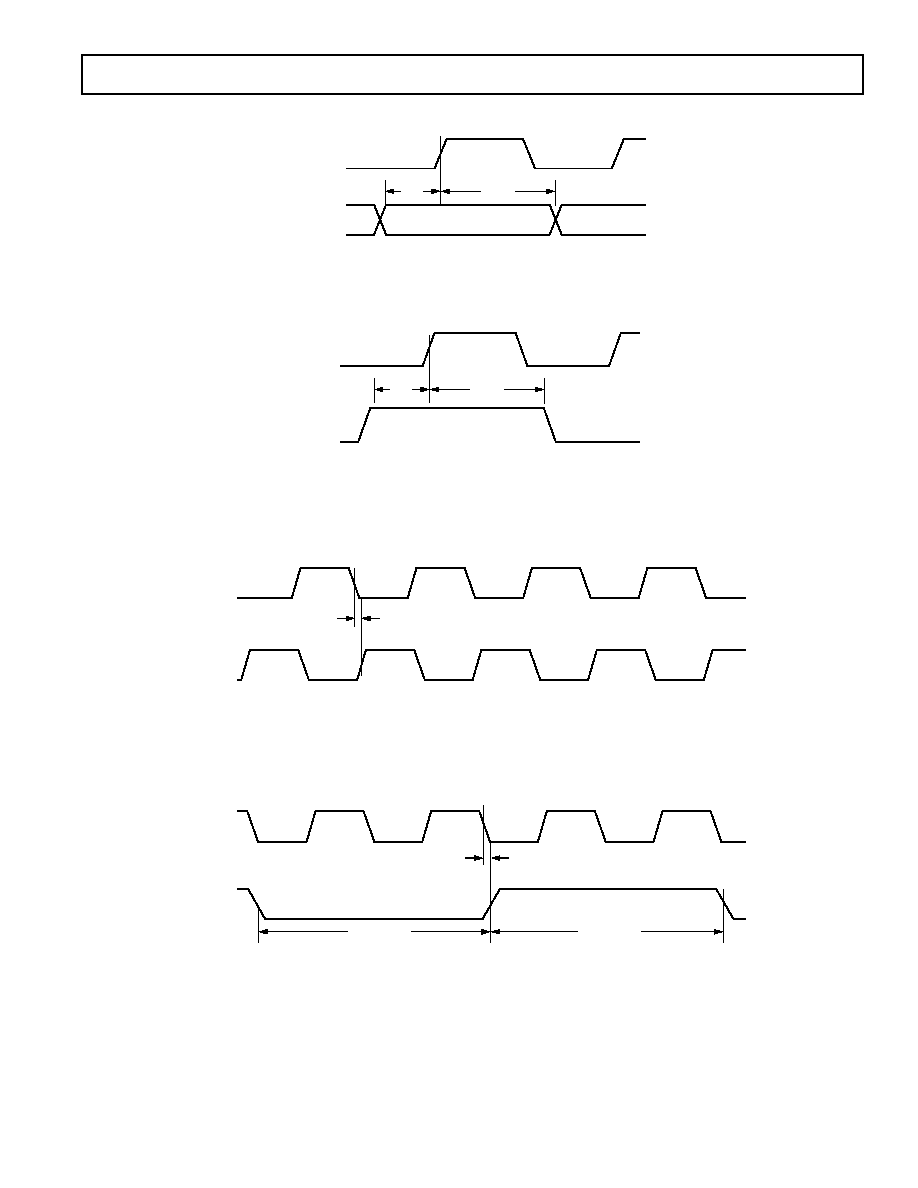
TIMING DIAGRAMS
CLKn
t
DLI
t
CLKL
t
CLK
t
CLKH
LIxy
Figure 3. Level Indicator Output Switching Characteristics (x = A, B, C, D; and y = A, B)
(For x = A and B, n = 0; and for x = C or D, n = 1)
RESET
t
RESL
Figure 4. Reset Timing Requirements
t
SCLKH
t
SCLKL
SCLKn
Figure 5. SCLK Switching Characteristics (n = 0, 4)
SCLKn
SDIn
DATA
t
SSI
t
HSI
Figure 6. Serial Port Input Timing Characteristics (n = 0, 4)
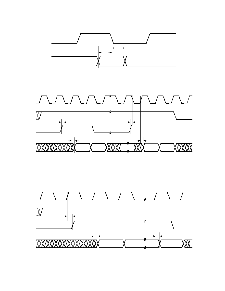
REV. 0
AD6635
17
CLKn
INx[13:0]
EXPx[2:0]
IENx
t
HI
t
SI
Figure 7. Input Timing for A and B Channels
t
HS
t
SS
CLKn
SYNCA
SYNCB
SYNCC
SYNCD
Figure 8. SYNC Timing Inputs
CLKn
PCLKn
t
DPOCLKL
Figure 9. PCLKn to CLKn Switching Characteristics Divide by 1
CLKn
PCLKn
t
DPOCLKLL
t
POCLKL
t
POCLKLH
Figure 10. PCLKn to CLKn Switching Characteristics Divide by 2, 4, or 8
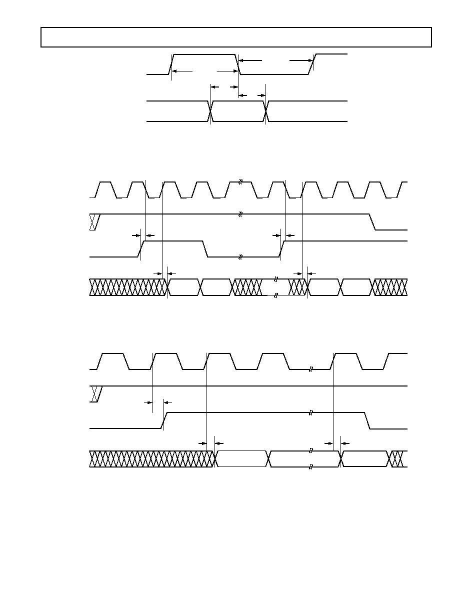
REV. 0
18
AD6635
PCLKn
PxACK
t
SPA
t
HPA
Figure 11. Master Mode PxACK to PCLKn Setup and Hold Characteristics
(n = 0 and x = A, B; or n = 1 and x = C, D)
DATA 1
DATA 2
DATA N1
DATA N
PCLKn
PxREQ
PxACK
Px[15:0]
t
SPA
t
DPP
t
SPA
t
DPP
Figure 12. Master Mode PxACK to PCLKn Switching Characteristics
(n = 0 and x = A, B; or n = 1 and x = C, D)
PCLKn
DATA 1
DATA N
t
DPP
t
DPP
t
DPREQ
PxACK
PxREQ
Px[15:0]
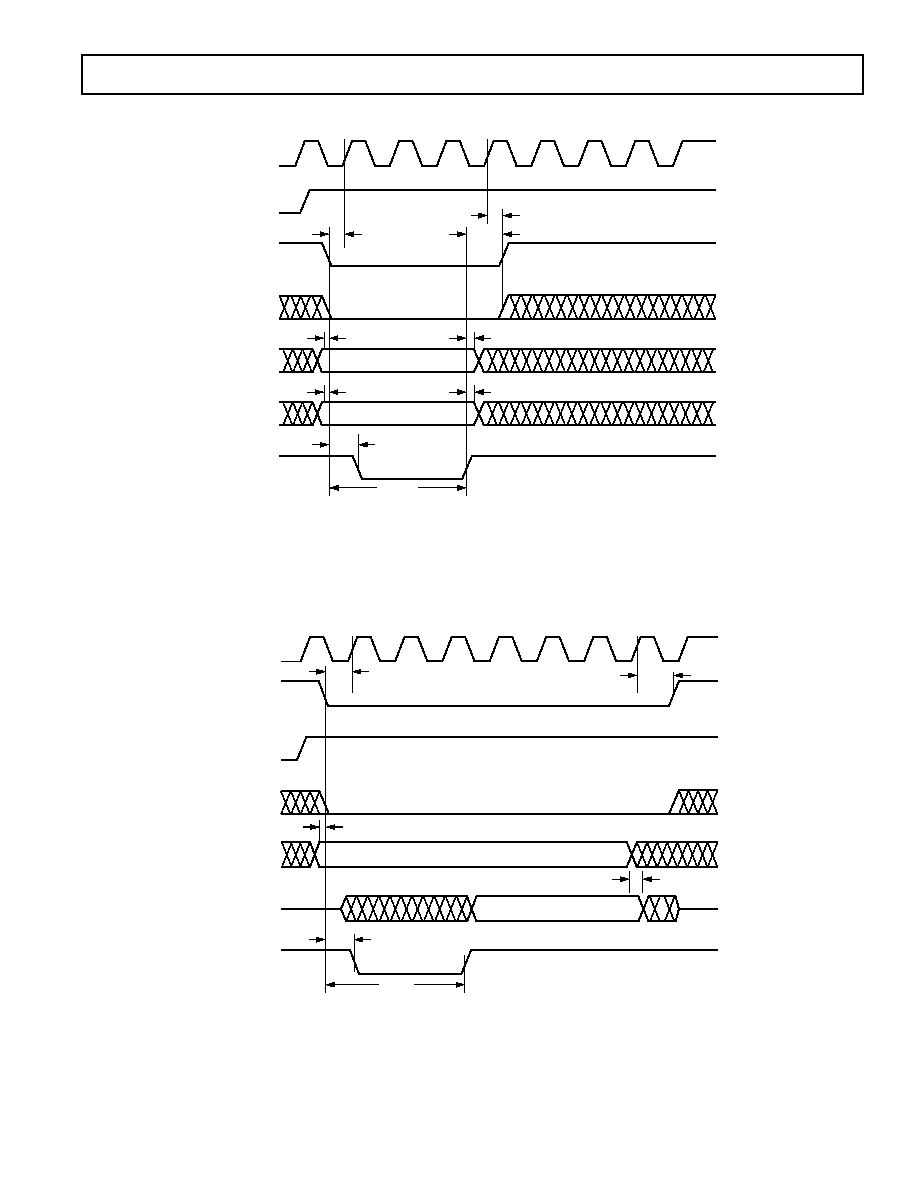
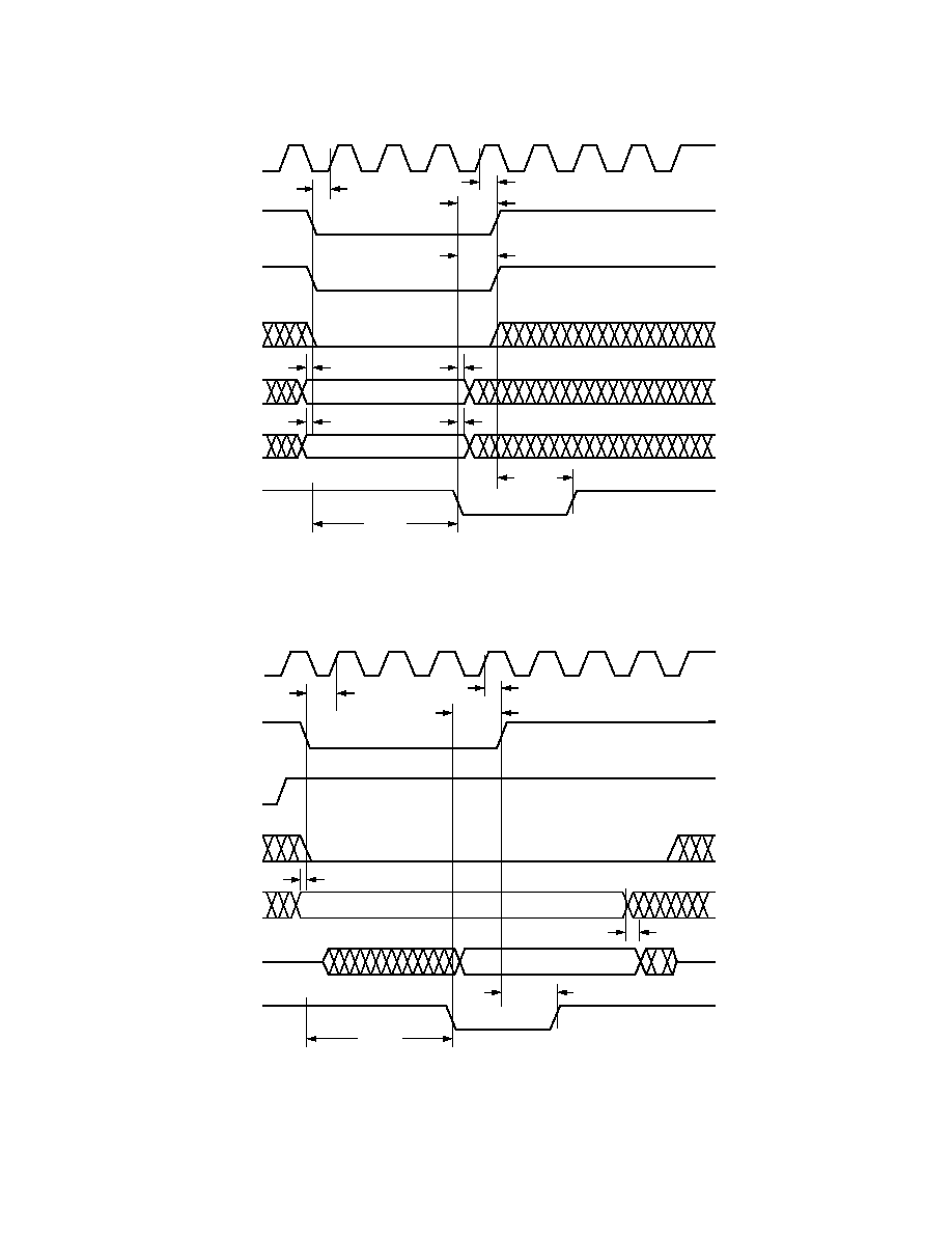
Figure 13. Master Mode PxREQ to PCLKn Switching Characteristics
(n = 0 and x = A, B; or n = 1 and x = C, D)
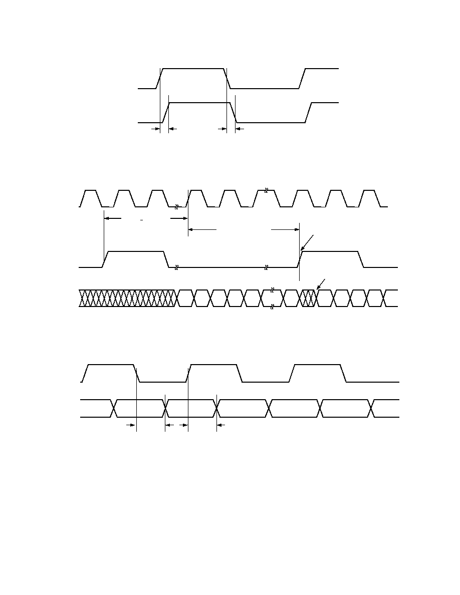
REV. 0
AD6635
19
t
SPA
t
HPA
t
POCLKL
t
POCLKH
PCLKn
PxACK
Figure 14. Slave Mode PxACK to PCLKn Setup and Hold Characteristics
(n = 0 and x = A, B; or n = 1 and x = C, D)
DATA 1
DATA 2
DATA N1
DATA N
PCLKn
PxREQ
PxACK
Px[15:0]
t
SPA
t
DPP
t
SPA
t
DPP
Figure 15. Slave Mode PxACK to PCLKn Switching Characteristics
(n = 0 and x = A, B; or n = 1 x = C, D)
PCLKn
DATA 1
DATA N
t
DPP
t
DPP
t
DPREQ
PxACK
PxREQ
Px[15:0]
Figure 16. Slave Mode PxREQ to PCLKn Switching Characteristics
(n = 0 and x = A, B; or n = 1 and x = C, D)
REV. 0
20
AD6635
PCLKn
LxCLKOUT
t
RDLCLK
t
FDLCLK
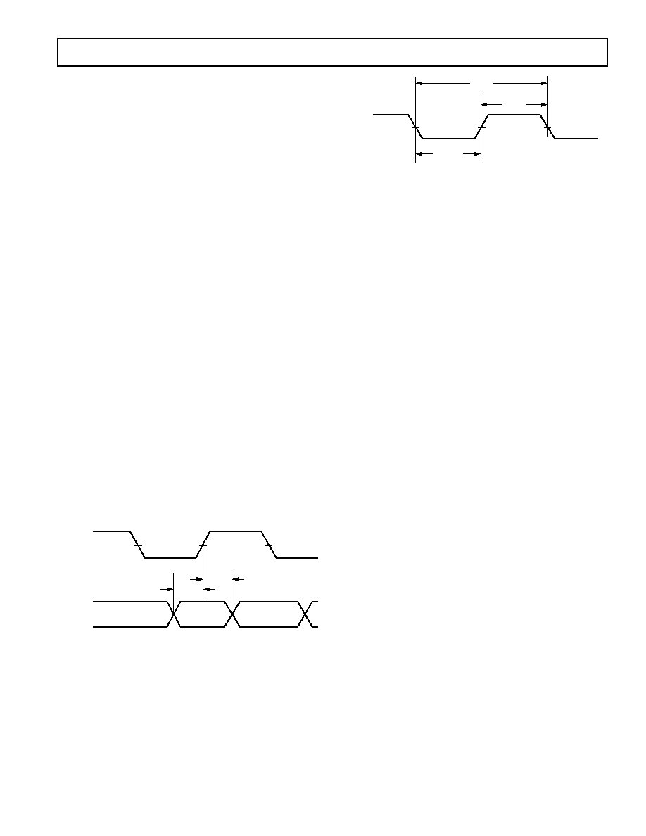
Figure 17. LxCLKOUT to PCLKn (n = 0 and x = A, B; or n = 1 and x = C, D) Switching Characteristics
LxCLKOUT
LxCLKIN
Lx[7:0]
WAIT > 6 CYCLES
ONE TIME CONNECTIVITY CHECK
NEXT TRANSFER
ACKNOWLEDGE
NEXT TRANSFER
BEGINS
8 LxCLKOUT CYCLES
D0
D1
D2
D3
D4
D15
D0
D1
D2
D3
Figure 18. LxCLKIN to LxCLKOUT Data Switching Characteristics
LxCLKOUT
Lx[7:0]
t
FDLCLKDAT
t
RDLCLKDAT
Figure 19. LxCLKOUT to Lx[7:0] Data Switching Characteristics
REV. 0
AD6635
21
TIMING DIAGRAMS INM Microport Mode (MODE = 0)
CLK0
CLK1
RD (DS)
WR (RW)
CS0
CS1
A[2:0]
D[7:0]
RDY
(
DTACK)
VALID ADDRESS
VALID DATA
NOTES
1.
t
ACC
ACCESS TIME DEPENDS ON THE ADDRESS ACCESSED. ACCESS TIME IS MEASURED
FROM FE OF
WR TO RE OF RDY.
2.
t
ACC
REQUIRES A MAXIMUM OF 9 CLK PERIODS.
t
SC
t
HC
t
HWR
t
HAM
t
SAM
t
HAM
t
SAM
t
DRDY
t
ACC
Figure 20. INM Microport Write Timing Requirements. CLK0 corresponds to
CS0, and CLK1 to CS1.
CS0 and CS1 both active (low) at the same time will cause errors in writing.
t
SC
CLK0
CLK1
RD (DS)
WR (RW)
A[2:0]
D[7:0]
RDY
(
DTACK)
CS0
CS1
NOTES
1.
t
ACC
ACCESS TIME DEPENDS ON THE ADDRESS ACCESSED. ACCESS TIME IS MEASURED
FROM FE OF
WR TO RE OF RDY.
2.
t
ACC
REQUIRES A MAXIMUM OF 13 CLK PERIODS AND APPLIES TO A[2:0] = 7, 6, 5, 3, 2, 1.
t
HC
t
SAM
t
HAM
VALID ADDRESS
VALID DATA
t
DRDY
t
ACC
Figure 21. INM Microport Read Timing Requirements. CLK0 corresponds to
CS0, and CLK1 to CS1.
CS0 and CS1 both active (low) at the same time will cause contention on data bus.
REV. 0
22
AD6635
TIMING DIAGRAMS MNM Microport Mode (MODE = 1)
VALID ADDRESS
VALID DATA
CLK0
CLK1
DS (RD)
RW (
WR)
CS0
CS1
A[2:0]
D[7:0]
DTACK
(RDY)
NOTES
1.
t
ACC
ACCESS TIME DEPENDS ON THE ADDRESS ACCESSED. ACCESS TIME IS MEASURED
FROM FE OF
DS TO THE FE OF DTACK.
2.
t
ACC
REQUIRES A MAXIMUM OF 9 CLK PERIODS.
t
SC
t
HC
t
HDS
t
HRW
t
HAM
t
ACC
t
SAM
t
HAM
t
SAM
t
DDTACK
Figure 22. MNM Microport Write Timing Requirements. CLK0 corresponds to
CS0, and CLK1 to CS1.
CS0 and CS1 both active (low) at the same time will cause errors in writing.
CLK0
CLK1
DS (RD)
RW (
WR)
A[2:0]
D[7:0]
DTACK
(RDY)
t
SC
t
ACC
t
DDTACK
NOTES
1.
t
ACC
ACCESS TIME DEPENDS ON THE ADDRESS ACCESSED. ACCESS TIME IS MEASURED
FROM THE FE OF
DS TO THE FE OF DTACK.
2.
t
ACC
REQUIRES A MAXIMUM OF 13 CLK PERIODS.
VALID ADDRESS
VALID DATA
t
SAM
t
HC
t
HDS
t
HAM
CS0
CS1
Figure 23. MNM Microport Read Timing Requirements. CLK0 corresponds to
CS0, and CLK1 to CS1.
CS0 and CS1 both active (low) at the same time will cause contention on data bus.
REV. 0
AD6635
23
INPUT DATA PORTS
The AD6635 features four high speed ADC Input Ports, A, B,
C, and D. The input ports allow for the most flexibility with a
single tuner chip. These can be diversity inputs or truly inde-
pendent inputs such as separate antenna segments. Channels 0
through 3 can take data from either of the input ports A or B
independently. Similarly, Channels 4 through 7 can take data
from either of the Input Ports C or D independently. For added
flexibility, each input port can be used to support multiplexed
inputs, such as found on the AD6600 or other ADCs with multi-
plexed outputs. This added flexibility allows up to eight different
analog sources to be processed simultaneously by the eight
internal AD6635 channels.
In addition, the front end of the AD6635 contains circuitry that
enables high speed signal level detection and control. This is
accomplished with a unique high speed level detection circuit
that offers minimal latency and maximum flexibility to control
up to four analog signal paths. The overall signal path latency
from input to output on the AD6635 can be expressed in high
speed clock cycles. The equation below can be used to calculate
the latency.
T
M
M
N
LATENCY
rCIC
CIC
TAPS
=
+ +
+
2
5
7
26
(
)
M
rCIC2
and M
CIC5
are decimation values for the rCIC2 and CIC5
filters, respectively. N
TAPS
is the number of RCF taps chosen.
Input Data Format
Each input port consists of a 14-bit mantissa and 3-bit exponent. If
interfacing to a standard ADC, the exponent bits can be grounded.
If connected to a floating point ADC, such as the AD6600, the
exponent bits from that ADC product can be connected to the
input exponent bits of the AD6635. The mantissa data format is
twos complement, and the exponent is unsigned binary.
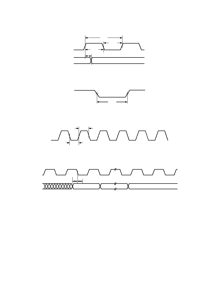
Input Timing
The data from each high speed input port is latched on the
rising edge of CLK. This clock signal is used to sample the
input port and clock the synchronous signal processing stages
that follow in the selected channels.
CLK
IN[13:0]
EXP[2:0]
DATA
t
SI
t
HI
Figure 24. Input Data Timing Requirements
The clock signals can operate up to 80 MHz and have a 50%
duty cycle. In applications using high speed ADCs, the ADC
sample clock or data valid strobe is typically used to clock the
AD6635.
t
CLKL
t
CLK
t
CLKH
CLKn
Figure 25. CLKn Timing Requirements (n = 0, 1)
Input Enable Control
There are four Input Enable pins IENx (x = A, B, C, or D)
corresponding to individual Input Ports A through D. There are
four modes of operation possible while using each IEN pin.
Using these modes, it is possible to emulate operation of the
other RSPs such as the AD6620, which offer dual channel
modes normally associated with diversity operations. These
modes are IEN transition to Low, IEN transition to High, IEN
High, and Blank on IEN Low.
In the IEN High mode, the inputs and normal operations occur
when the Input Enable is High. In the IEN transition to Low
mode, normal operations occur on the first rising edge of the
clock after the IEN transitions to Low. Likewise in the IEN
transition to High mode, operations occur on the rising edge of
the clock after the IEN transitions to High. See the numerically
Controlled Oscillator section for more details on configuring the
Input Enable Modes. In Blank on IEN Low mode, the input
data is interpreted as zero when IEN is low.
A typical application for input modes would be to take the data
from an AD6600 Diversity ADC to one of the inputs of the
AD6635. The A/B_OUT from that chip would be tied to the
IEN of the corresponding input port. Then one channel within
the AD6635 would be set so that IEN transition to Low is
enabled. Another channel would be configured so that IEN
transition to High is enabled. This would allow two of the
AD6635 channels to be configured to emulate that AD6620 in
diversity mode and receive interleaved input data. Though the
NCO frequencies and other channel characteristics would need
to be set similarly, this feature allows the AD6635 to handle
interleaved data streams such as found on the AD6600.
The difference between the IEN transition to High and the
IEN High is found when a system clock is provided that is
higher than the data rate of the converter. It is often advanta-
geous to supply a clock that runs faster than the data rate so
that additional filter taps can be computed. This indeed leads
to better filtering. To ensure that other parts of the circuit
properly recognize the faster clock in the simplest manner,
the IEN transition to Low or High should be used. In this
mode, only the first clock edge that meets the setup and hold
times will be used to latch and process the input data. All other
clocks pulses are ignored by front end processing. However,
each clock cycle will still produce a new filter computation pair.
Gain Switching
The AD6635 includes circuitry that is useful in applications where
either large dynamic ranges exist, or where gain ranging converters
are employed. This circuitry allows digital thresholds to be set such
that an upper and a lower threshold can be programmed.
One such use of this may be to detect when an ADC is about to
reach full scale with a particular input condition. The results
REV. 0
24
AD6635
would be to provide a flag that could be used to quickly insert
an attenuator that would prevent ADC overdrive. If 18 dB (or
any other arbitrary value) of attenuation is switched in, then the
signal dynamic range of the system will have been increased by
18 dB. The process begins when the input signal reaches the
upper programmed threshold. In a typical application, this may
be set 1 dB (user definable) below full scale. When this input
condition is met, the appropriate LI signal (LIA-A, LIB-A, LIC-A,
or LID-A) associated with its corresponding input port (A through
D) is made active. This can be used to switch the gain or attenua-
tion of the external circuit. The LI line stays active until the input
condition falls below the lower programmed threshold. To provide
hysteresis, a dwell time register (see Memory Map for Input Con-
trol Registers) is available to hold off switching of the control line
for a predetermined number of clocks. Once the input condition is
below the lower threshold, the programmable counter begins
counting high speed clocks. As long as the input signal stays
below the lower threshold for the number of high speed clock
cycles programmed, the attenuator will be removed on the
terminal count. However, if the input condition goes above
the lower threshold with the counter running, the counter is
reset and input must fall below the lower threshold again to
initiate the process. This will prevent unnecessary switching
between states.
This is illustrated in Figure 26. When the input signal goes
above the upper threshold, the appropriate LI signal becomes
active. Once the signal falls below the lower threshold, the
counter begins counting. If the input condition goes above the
lower threshold, the counter is reset and starts again as shown.
Once the counter has terminated to 0, the LI line goes inactive.
"HIGH"
MANTISSA
DWELL TIME
"LOW"
UPPER
THRESHOLD
LOWER
THRESHOLD
COUNTER
RESTARTS
TIME
Figure 26. Threshold Settings for LI
The LI line can be used for a variety of functions. It can be used
to set the controls of an attenuator, DVGA, or it can be inte-
grated and used with an analog VGA. To simplify the use of this
feature, the AD6635 includes two separate gain settings, one
when this LI line is inactive (rCIC2_QUIET[4:0] stored in Bits 9:5
of 0x92 register) and the other when active (rCIC2_LOUD[4:0]
stored in Bits 4:0 of 0x92 register). This allows the digital gain to
be adjusted to the external changes. In conjunction with the
gain setting, a variable holdoff is included to compensate for the
pipeline delay of the ADC and the switching time of the gain
control element. Together, these two features provide seamless
gain switching.
Another use of this pin is to facilitate a gain-range holdoff within a
gain-ranging ADC. For converters that use gain-ranging to
increase total signal dynamic range, it may be desirable to prohibit
internal gain ranging from occurring in some instances. For such
converters, the LI (A or B) line can be used to hold this off. For
this application, the upper threshold would be set based on similar
criteria. However, the lower threshold would be set to a level
consistent with the gain ranges of the specific converter. Then
the holdoff delay can be set appropriately for any of a number of
factors, such as fading profile, signal peak-to-average ratio, or
any other time based characteristics that might cause unnecessary
gain changes.
The AD6635 has a total of eight gain control circuits to support
all channels, and hence can be used even when all input ports
have interleaved data. When data is interleaved on a certain
input port, the appropriate bit should be set in the Gain Range
Control Register. This way both interleaved channel data can be
monitored, and LIA-B, LIB-B, LIC-B, or LID-B pins associ-
ated with their corresponding Input Ports A through D act as
output indicators for the interleaved channel. LIx-A pins act as
indicators for input data corresponding to IENx Low, and LIx-B
act as indicators for input data corresponding to IENx High in
this mode. When interleaved channels are not used, LIx-B pins
are complimentary to LIx-A pins acting as indicators with oppo-
site polarity. It should be noted that the gain control circuits are
wideband and are implemented prior to any filtering elements to
minimize loop delay.
The chip also provides appropriate scaling of the internal data
based on the attenuation associated with the LI signal. In this
manner, data to the DSP maintains a correct scale value through-
out the process, making it entirely independent. Since there
often are finite delays associated with external gain switching
components, the AD6635 includes a variable pipeline delay that
can be used to compensate for external pipeline delays or gross
settling times associated with gain/attenuator devices. This delay
may be set for up to seven high speed clocks. These features
ensure smooth switching between gain settings.
Input Data Scaling
The AD6635 has four data input ports. Each accepts a 14-bit
mantissa (twos complement integer) IN[13:0], a 3-bit exponent
(unsigned integer) EXP[2:0], and the Input Enable(IEN). Input
Ports A and B are clocked by CLK0 and Input Ports C and D
are clocked by CLK1. These pins allow direct interfacing to both
standard fixed-point ADCs such as the AD9238 and AD6645, as
well as to gain-ranging ADCs such as the AD6600. For normal
operation with ADCs having fewer than 14 bits, the active bits
should be MSB justified and the unused LSBs should be tied low.
The 3-bit exponent, EXP[2:0] is interpreted as an unsigned
integer. The exponent will subsequently be modified by either
of rCIC2_LOUD[4:0] or rCIC2_QUIET[4:0], depending on
whether the LI line is active or not. These 5-bit scale values are
stored in the rCIC2 scale register (0x92) and the scaling is applied
before the data enters the rCIC2 resampling filter. These 5-bit
registers contain scale values to compensate for the rCIC2 gain,
external attenuator (if used), and the Exponent Offset (Expoff). If
no external attenuator is used, both the rCIC2_QUIET and
rCIC2_LOUD registers contain the same value. A detailed
explanation and equation for setting the attenuating scale
register is given in the Scaling with Floating-Point ADCs section.
Scaling with Fixed-Point ADCs
For fixed-point ADCs the AD6635 exponent inputs, EXP[2:0],
are typically not used and should be tied low. The ADC outputs
are tied directly to the AD6635 inputs, MSB-justified. The
ExpOff bits in 0x92 should be programmed to 0. Likewise, the
Exponent Invert bit should be 0. Thus for fixed-point ADCs,
the exponents are typically static and no input scaling is used in
the AD6635.
REV. 0
AD6635
25
IN13
IN2
IN1
IN0
EXP2
EXP1
EXP0
IEN
VDD
D11 (MSB)
D0 (LSB)
AD6645
AD6635
(ExpOff = 0, ExpInv = 0)
Figure 27. Typical Interconnection of the AD6645
Fixed-Point ADC and the AD6635
Scaling with Floating-Point or Gain-Ranging ADCs
An example of the exponent control feature combines the
AD6600 and the AD6635. The AD6600 is an 11-bit ADC with
3 bits of gain ranging. In effect, the 11-bit ADC provides the
mantissa, and the 3 bits of relative signal strength indicator
(RSSI) for the exponent. Only five of the eight available steps
are used by the AD6600. See the AD6600 data sheet for addi-
tional details.
For gain-ranging ADCs such as the AD6600,
scaled
input
in
Exp rCIC
_
mod(
,
)
= ¥
+
2
7
2 32
ExpInv = 1, ExpWeight = 0
where IN is the value of IN[13:0], Exp is the value of EXP[2:0],
and rCIC2 is the rCIC scale register value (0x92 bits 9-5 and 4-0).
"mod" is the remainder function. For example, mod(1,32) = 1,
mod(2,32) = 2, and mod(34,32) = 2.
The RSSI output of the AD6600 grows numerically with increas-
ing signal strength of the analog input (RSSI = 5 for a large
signal, RSSI = 0 for a small signal). When the Exponent Invert
Bit (ExpInv) is set to zero, the AD6635 will consider the small-
est signal at the IN[13:0] to be the largest, and as the EXP word
increases, it shifts the data down internally (EXP = 5 will shift a
14-bit word to the right by 5 internal bits before passing the
data to the rCIC2). In this example, if ExpInv = 0, the AD6635
regards the RSSI[2:0] = 5 as smallest signal and RSSI[2:0] = 0
as the largest signal possible on the AD6600. Thus, we can use
the Exponent Invert Bit to make the AD6635 exponent agree
with the AD6600 RSSI. Setting ExpInv = 1 forces the AD6635
to shift the data up (left) for growing EXP instead of down.
The exponent invert bit should always be set high for use
with the AD6600.
The Exponent Offset is used to shift the data up. For example,
Table I shows that with no rCIC2 scaling, 12 dB of range is
lost when the ADC input is at the largest level. This is not
desired because it lowers the dynamic range and SNR of the
system by reducing the signal of interest relative to the quan-
tization noise floor.
Table I. AD6600 Transfer Function with
AD6635 ExpInv = 1, and no ExpOff
ADC
Signal
Input
AD6600
AD6635
Reduction
Level
RSSI[2:0]
Data
(dB)
Largest
101 (5)
/4 (>> 2)
12
100 (4)
/8 (>>3)
18
011 (3)
/16 (>> 4)
24
010 (2)
/32 (>> 5)
30
001 (1)
/64 (>> 6)
36
Smallest
000 (0)
/128(>> 7)
42
ExpInv = 1, rCIC2 Scale = 0)
To avoid this automatic attenuation of the full-scale ADC sig-
nal, the ExpOff is used to move the largest signal (RSSI = 5) up
to the point where there is no downshift. In other words, once
the Exponent Invert bit has been set, the Exponent Offset should
be adjusted so that mod(7-5 + ExpOff,32) = 0. This is the case
when Exponent Offset is set to 30 since mod(32,32) = 0. Table II
illustrates the use of ExpInv and ExpOff when used with the
AD6600 ADC.
Table II. AD6600 Transfer Function with
AD6620 ExpInv = 1, and ExpOff = 30
ADC
Signal
Input
AD6600
AD6635
Reduction
Level
RSSI[2:0]
Data
(dB)
Largest
101 (5)
/1 (>> 0)
0
100 (4)
/2 (>>1)
6
011 (3)
/4 (>> 2)
12
010 (2)
/8 (>> 3)
18
001 (1)
/16 (>> 4)
24
Smallest
000 (0)
/32(>> 5)
30
ExpInv = 1, ExpOff = 30, Exp Weight = 0)
This flexibility in handling the exponent allows the AD6635 to
interface with other gain-ranging ADCs besides the AD6600.
The Exponent Offset can be adjusted to allow up to seven
RSSI(EXP) ranges to be used as opposed to the AD6600's five.
It also allows the AD6635 to be tailored in a system that employs
the AD6600 but does not utilize all of its signal range. For
example, if only the first four RSSI ranges are expected to
occur, then the ExpOff could be adjusted to 29, which would
make RSSI = 4 correspond to the 0 dB point of the AD6635.
Note that the above scale factor set in the rCIC2 register is only
to account for the ExpOff required. This register should also
account for compensating rCIC2 filter gain. The value required
for this will be given in the CIC2 filter section. Hence the final
value set in the rCIC2 register will be the sum total of ExpOff
and rCIC2 scale required.
REV. 0
26
AD6635
IN13
IN2
IN1
IN0
IEN
D10 (MSB)
D0 (LSB)
AD6600
AD6635
EXP1
RSSI1
EXP2
RSSI2
EXP0
RSSI0
AB_OUT
Figure 28. Typical Interconnection of the AD6600
Gain-Ranging ADC and the AD6635.
NUMERICALLY CONTROLLED OSCILLATOR
Frequency Translation
This processing stage comprises a digital tuner consisting of two
multipliers and a 32-bit complex NCO. Each channel of the
AD6635 has an independent NCO. The NCO serves as a quadra-
ture local oscillator capable of producing an NCO frequency
between CLK/2 and +CLK/2 with a resolution of CLK/2
32
in the
complex mode. The worst-case spurious signal from the NCO is
better than 100 dBc for all output frequencies.
The NCO frequency value in registers 0x85 and 0x86 are inter-
preted as a 32-bit unsigned integer. The NCO frequency is
calculated using the equation below.
NCO FREQ
f
CLKn
CHANNEL
_
mod
,
=
¥
Ê
Ë
Á
^
¯
~
2
1
32
where NCO_FREQ is the 32-bit integer (registers 0x85 and
0x86) that the user needs to set in order to tune to a desired
frequency f
CHANNEL
, and CLKn is the AD6635 master clock rate
or Input data rate, depending on the Input Enable mode used.
See the Input Enable Control section to determine when it is
CLK and when it is Input data rate. For Channels 0 through 3
use CLK0, and for Channels 4 through 7 use CLK1.
"mod" is similar to the remainder function. For example if
f
CHANNEL
= 220 MHz and CLK = 80 MHz, then mod(220/80,1)
= mod(2.75,1) = 0.75.
But for negative frequencies, for example,
mod(220/80,1) = mod(1.75,1) = 0.25.
This definition works if NCO_FREQ register is treated as a
signed number.
NCO Frequency Holdoff Register
When the NCO frequency registers are written, data is actually
passed to a shadow register. Data may be moved to the main
registers by one of two methods: when the channel comes out of
sleep mode, or when a SYNC hop occurs. In either event, a
counter can be loaded with the NCO Frequency Holdoff regis-
ter value. The 16-bit unsigned integer counter (0x84) starts
counting down, clocked by the Master clock, and when it reaches
zero, the new frequency value in the shadow register is written
to the NCO frequency register. The NCO could also be set up
to SYNC immediately, in which case the Frequency Holdoff
counter is bypassed (by writing a value of 1) and new frequency
values are updated immediately. If a zero is written, then SYNC
will never occur.
Phase Offset
The Phase Offset register (0x87) adds an offset to the phase
accumulator of the NCO. The NCO phase accumulator starts
with the value in this register in the event of a START SYNC.
This is a 16-bit register and is interpreted as a 16-bit unsigned
integer. A 0x0000 in this register corresponds to a 0 radian
offset, and a 0xFFFF corresponds to an offset of 2
¥ (1 1/(2
16
))
radians. This register allows multiple NCOs to be synchronized to
produce sine waves with a known and steady phase difference.
NCO Control Register
The NCO control register located at 0x88 is used to configure
the features of the NCO. These are controlled on a per channel
basis and are described below.
Bypass
The NCO in the front end of the AD6635 can be bypassed.
Bypass mode is enabled by setting Bit 0 of 0x88 high. When the
NCO is bypassed, down conversion is not performed and the
AD6635 channel functions simply as a real filter on complex
data. This is useful for a baseband sampling application where
the A input is connected to the I signal path within the filter,
and the B input is connected to the Q signal path for Channels 0
through 3. Similarly, input C is connected to I signal path and
input D to Q signal path for Channels 4 through 7. This may be
desired if the digitized signal has already been converted to
baseband in prior analog stages or by other digital preprocessing.
Phase Dither
The AD6635 provides a phase dither option for improving the
spurious performance of the NCO. Phase dither is enabled by
setting Bit 1 of the NCO control register. When phase dither is
enabled by setting this bit high, spurs due to phase truncation in
the NCO are randomized. The energy from these spurs is
spread into the noise floor and spurious-free dynamic range is
increased at the expense of very slight decreases in the SNR.
The choice of whether phase dither is used in a system will
ultimately be decided by the system goals. If lower spurs are
desired at the expense of a slightly raised noise floor, it should
be employed. If a low noise floor is desired and the higher spurs
can be tolerated or filtered by subsequent stages, phase dither is
not needed.
Amplitude Dither
Amplitude dither can also be used to improve spurious perfor-
mance of the NCO. Amplitude dither is enabled by setting Bit 2.
Amplitude dither improves performance by randomizing the
amplitude quantization errors within the angular-to-Cartesian
conversion of the NCO. This option may reduce spurs at the
expense of a slightly raised noise floor. Amplitude dither and phase
dither can be used together, separately, or not at all.
Clear Phase Accumulator on Hop
When Bit 3 is set, the NCO phase accumulator is cleared prior
to a frequency hop. This ensures a consistent phase of the NCO
on each hop. The NCO phase offset is unaffected by this setting
and is still in effect. If phase-continuous hopping is desired, this
bit should be cleared and the last phase in the NCO phase regis-
ter will be the initiating point for the new frequency.
Input Enable Control
There are four different modes of operation for the input enable.
Each of the high speed input ports includes an IEN line. Any of
the four filter Channels 0 through 3 can be programmed to take
data from either of the two Input Ports A or B (see the WB
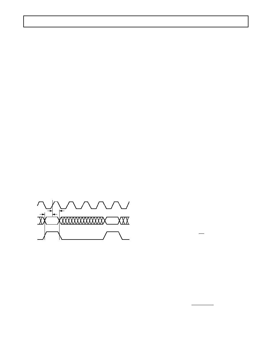
REV. 0
AD6635
27
Input Select section). Similarly, any of the four filter Channels
4 through 7 can be programmed to take data from either of the
two Input Ports C or D. Along with data is the IENx signal. Each
filter channel can be configured to process the IEN signal in one
of four modes. Three of the modes are associated with when
data is processed based on a time division multiplexed data
stream. The fourth mode is used in applications that employ time
division duplex, such as radar, sonar, ultrasound, and com-
munications that involve TDD.
Mode 00: Blank on IEN Low
In this mode, data is blanked while the IEN line is low. While
the IEN line is high, new data is strobed on each rising edge of
the input clock. When the IEN line is lowered, input data is
replaced with zero values. During this period, the NCO contin-
ues to run such that when the IEN line is raised again, the
NCO value will be at the same value it would have been had the
IEN line never been lowered. This mode has the effect of blank-
ing the digital inputs when the IEN line is lowered. Back end
processing (rCIC2, CIC5, and RCF) continues while the IEN
line is high. This mode is useful for time division multiplexed
applications.
Mode 01: Clock on IEN High
In this mode, data is clocked into the chip while the IEN line is
high. While the IEN line is high, new data is strobed on each
rising edge of the input clock. When the IEN line is lowered,
input data is no longer latched into the channel. Additionally,
NCO advances are halted. However, back end processing
(rCIC2, CIC5, and RCF) continues during this period. The
primary use for this mode is to allow for a clock that is faster
than the input sample data rate so that more filter taps can be
computed than would otherwise be possible. In the diagram
below, input data is strobed only while IEN is high, despite the
fact that the CLK continues to run at a rate four times faster
than the data.
n + 1
n
IN[13:0]
E[2:0]
CLK
IEN
t
SI
t
HI
Figure 29. Fractional Rate Input Timing (4
¥ CLK)
in Mode 01
Mode 10: Clock on IEN Transition to High
In this mode, data is clocked into the chip only on the first
clock edge after the rising transition of the IEN line. Although
data is only latched on the first valid clock edge, the back end
processing (rCIC2, CIC5, and RCF) continues on each avail-
able clock that may be present, similar to Mode 01. The NCO
phase accumulator is incremented only once for each new input
data sample, not once for each input clock.
Mode 11: Clock on IEN Transition to Low
In this mode, data is clocked into the chip only on the first clock
edge after the falling transition of the IEN line. Although data is
only latched on the first valid clock edge, the back end process-
ing (rCIC2, CIC5, and RCF) continues on each available clock
that may be present, similar to Mode 01. The NCO phase accu-
mulator is incremented only once for each new input data sample,
not once for each input clock.
WB Input Select
Bit 6 in this register controls which input port is selected for
signal processing. For Channels 0 through 3, if this bit is set
high, then Input Port B (INB, EXPB, and IENB) is connected
to the selected AD6635 channel. If this bit is cleared, Input Port A
(INA, EXPA, and IENA) is connected to the selected filter
channel. Similarly for Channels 4 through 7 Input Port D is
selected when Bit 6 is set and Input Port C is selected when this
bit is cleared.
Sync Select
Bits 7 and 8 of this register determine which external sync pin is
associated with the selected channel. The AD6635 has four sync
pins named SYNCA, SYNCB, SYNCC, and SYNCD. Any of
these sync pins can be associated with any of the eight receiver
channels within the AD6635. Additionally, if only one sync
signal is required for the system, all eight receiver channels can
reference the same sync pin. Bit value 00 selects SYNCA, 01
selects SYNCB, 10 selects SYNCC, and 11 selects SYNCD.
SECOND-ORDER rCIC FILTER
The rCIC2 filter is a second-order resampling Cascaded Inte-
grator Comb filter. The resampler is implemented using a
unique technique that does not require the use of a high speed
clock, thus simplifying the design and saving power. The
resampler allows noninteger relationships between the master
clock and the output data rate. This allows easier implementa-
tion of systems that are either multimode or require a master
clock that is not a multiple of the data rate to be used.
Interpolation up to 512 and decimation up to 4096 is allowed in
the rCIC2. The resampling factor for the rCIC2 (L) is a 9-bit
integer. When combined with the 12-bit decimation factor M,
the total rate change can be any fraction in the form of:
R
L
M
R
rCIC
rCIC
2
2
1
=
£
The only constraint is that the ratio L/M must be less than or
equal to 1. This implies that the rCIC2 decimates by 1 or more.
Resampling is implemented by apparently increasing the input
sample rate by the factor L using zero stuffing for the new data
samples. Following the resampler is a second-order cascaded
integrator comb filter. Filter characteristics are determined only
by the fractional rate change (L/M).
The filter can process signals at the full rate of the input port
80 MHz. The output rate of this stage is given by the equa-
tion below.
f
L
f
M
SAMP
rCIC
SAMP
rCIC
2
2
=
2

REV. 0
28
AD6635
Both L
rCIC2
and M
rCIC2
are unsigned integers. The interpolation
rate (L
rCIC2
) may be from 1 to 512 and the decimation (M
rCIC2
)
may be from 1 to 4096. The stage can be bypassed by setting
the decimation/interpolation to 1/1.
The frequency response of the rCIC2 filter is given by the fol-
lowing equations.
H z
L
z
z
SrCIC
rCIC
MrCIC
LrCIC
( )
=
¥
¥
Ê
Ë
Á
Á
Á
^
¯
~
~
~
1
2
1
1
2
2
2
2
1
2
H f
L
M
f
L
f
f
f
SrCIC
rCIC
rCIC
rCIC
SAMP
SAMP
( )
=
¥
¥
¥
¥
Ê
Ë
Á
^
¯
~
Ê
Ë
Á
^
¯
~
Ê
Ë
Á
Á
Á
Á
^
¯
~
~
~
~
1
2
2
2
2
2
2
sin
sin
p
p
The scale factor, S
rCIC2
is a programmable unsigned 5-bit value
between 0 and 31. This serves as an attenuator that can reduce
the gain of the rCIC2 in 6 dB increments. For the best dynamic
range, S
rCIC2
should be set to the smallest value possible (i.e.,
lowest attenuation) without creating an overflow condition.
This can be safely accomplished using the equation below,
where input_level is the largest fraction of full scale possible at
the input to the AD6635 (normally 1). The rCIC2 scale factor
is always used, whether or not the rCIC2 is bypassed.
S
ceil
M
floor
M
L
M
L
floor
M
L
rCIC
rCIC
rCIC
rCIC
rCIC
rCIC
rCIC
rCIC
2
2
2
2
2
2
2
2
2
2
1
=
+
Ê
Ë
Á
^
¯
~ ¥
¥
¥
+
Ê
Ë
Á
^
¯
~
Ê
Ë
Á
^
¯
~
Ê
Ë
Á
Á
Á
Á
^
¯
~
~
~
~
È
Î
Í
Í
Í
Í
Í
°
log
OL
M
L
input
level
CIC
rCIC
rCIC
SrCIC
2
2
2
2
2
2
=
(
)
¥
¥
_
The ceil function used above denotes the next whole integer,
and the floor function denotes the previous whole integer. For
example, ceil(4.5) is 5, while floor(4.5) is 4.
There are two scale registers (rCIC2_LOUD[4:0] Bits 40 in
0x92), and (rCIC2_QUIET[4:0] Bits 95 in 0x92), which are
used to implement the S
rCIC2
scale factor. The value written into
the these programmable registers is the sum total of S
rCIC2
, ExpOff
required for floating point ADCs (explained in the Input Port
section), and any compensation for external attenuation that
may be activated using the LI (level indicator) pins. The third
component can have different values when the LI pin is active
and when it is inactive, and hence two registers, rCIC2_LOUD
and rCIC2_QUIET. The sum total of these components is
supplied to the AD6635 as rCIC2_LOUD and rCIC2_QUIET
registers, and these registers can contain a maximum number of
31. It should also be noted that the scaling specified by these
register is applied at only one place in the AD6635 channel
(before the rCIC2 filter).
The gain and passband droop of the rCIC2 should be calculated
by the equations above, as well as the filter transfer equations
mentioned previously. Excessive passband droop can be com-
pensated for in the RCF stage by peaking the pass band by the
inverse of the roll-off.
scaled
input
IN
ExpInv
scaled
input
IN
ExpInv
Exp rCIC
Exp rCIC
_
,
_
,
mod(
,
mod(
,
=
¥
=
¥
+
+
2
2
2
7
2
32)
32)
= 0
= 1
where IN is the value of INx[13:0] (x = A, B, C, D), Exp is the
value of EXPx[2:0], and rCIC2 is the value of the 0x92
(rCIC2_QUIET[4:0] or rCIC2_LOUD[4:0], depending on
LI pin) scale register.
rCIC2 Rejection
Table III illustrates the amount of bandwidth in percent of the
data rate into the rCIC2 stage. The data in this table may be
scaled to any other allowable sample rate up to 80 MHz. The
table can be used as a tool to decide how to distribute the deci-
mation between rCIC2, CIC5 and the RCF.
Table III. SSB rCIC2 Alias Rejection Table (f
SAMP
= 1)
Bandwidth Shown as Percentage of f
SAMP.
(input rate)
M
rCIC2
/L
rCIC2
50 dB 60 dB 70 dB 80 dB
90 dB 100 dB
2
1.790
1.007
0.566
0.318
0.179
0.101
3
1.508
0.858
0.486
0.274
0.155
0.087
4
1.217
0.696
0.395
0.223
0.126
0.071
5
1.006
0.577
0.328
0.186
0.105
0.059
6
0.853
0.490
0.279
0.158
0.089
0.050
7
0.739
0.425
0.242
0.137
0.077
0.044
8
0.651
0.374
0.213
0.121
0.068
0.038
9
0.581
0.334
0.190
0.108
0.061
0.034
10
0.525
0.302
0.172
0.097
0.055
0.031
11
0.478
0.275
0.157
0.089
0.050
0.028
12
0.439
0.253
0.144
0.082
0.046
0.026
13
0.406
0.234
0.133
0.075
0.043
0.024
14
0.378
0.217
0.124
0.070
0.040
0.022
15
0.353
0.203
0.116
0.066
0.037
0.021
16
0.331
0.190
0.109
0.061
0.035
0.020
Example Calculations
Goal: Implement a filter with an input sample rate of 10 MHz
requiring 100 dB of alias rejection for a
±7 kHz pass band.
Solution: First determine the percentage of the sample rate that
is represented by the pass band.
BW
kHz
MHz
FRACTION
=
¥
=
100
7
10
0 07
.
In the 100 dB column on the right of the table, look for a
value greater than or equal to your passband percentage of the
clock rate. Then look across to the extreme left column and
find the corresponding rate change factor (M
rCIC2
/L
rCIC2)
. Referring
to the table, notice that for a M
rCIC2
/L
rCIC2
of 4, the frequency
having 100 dB of alias rejection is 0.071%, which is slightly
greater than the 0.07% calculated. Therefore, for this example,
the maximum bound on rCIC2 rate change is 4. Choosing a
higher M
rCIC2
/L
rCIC2
results in less alias rejection than the
required 100 dB.
An M
rCIC2
/L
rCIC2
of less than 4 would still yield the required
rejection, however the power consumption can be minimized by
decimating as much as possible in this rCIC2 stage. Decimation
in rCIC2 lowers the data rate, and thus reduces power consumed
in subsequent stages. It should also be noted that there is more
than one way to get the decimation of 4. A decimation of 4 is
the same as an L/M ratio of 0.25. Thus, any integer combination

REV. 0
AD6635
29
of L/M that yields 0.25 will work (1/4, 2/8, or 4/16). However,
for the best dynamic range, the simplest ratio should be used.
For example, 1/4 gives better performance than 4/16.
Decimation and Interpolation Registers
rCIC2 decimation values are stored in register 0x90. This 12-bit
register contains the decimation portion less 1. The interpola-
tion portion is stored in register 0x91. This 9-bit value holds the
interpolation less 1.
rCIC2 Scale
Register 0x92 contains the scaling information for this section of
the circuit. The primary function is to store the scale value
computed in the sections above.
Bits 40 (rCIC2_LOUD[4:0]) of this register are used to contain
the scaling factor for the rCIC2 during conditions of strong
signals. These five bits represent the rCIC2 scalar calculated
above, plus any external signal scaling with an attenuator.
Bits 95 (rCIC2_QUIET[4:0]) of this register are used to con-
tain the scaling factor for the rCIC2 during conditions of weak
signals. In this register, no external attenuator would be consid-
ered and is not included. Only the value computed above for
rCIC2 compensation is stored in these bits.
Bit 10 of this register is used to indicate the value of the external
exponent. If this bit is set low, then external exponent represents
6 dB per step as in the AD6600. If this bit is set high, each
exponent represents a 12 dB step.
Bit 11 of this register is used to invert the external exponent
before internal calculation. This bit should be set high for gain-
ranging ADCs that use an increasing exponent to represent an
increasing signal level. This bit should be set low for gain-ranging
ADCs that use a decreasing exponent for representing an
increasing signal level.
In applications that do not require the features of the rCIC2, it
may be bypassed by setting the L/M ratio to 1/1. This effectively
bypasses all circuitry of the rCIC2 except the scaling which is
still in effect.
FIFTH-ORDER CIC FILTER
The third signal processing stage, CIC5, implements a sharper,
fixed-coefficient, decimating filter sharper than rCIC2. The
input rate to this filter is f
SAMP2
. The maximum input rate to this
filter is equal to the input rate into the AD6635, so bypassing
the rCIC2 filter is allowed.
The decimation ratio, MCIC5, may be programmed from 2 to
32 (all integer values). The frequency response of the filter is
given by the following equations. The gain and passband droop
of CIC5 should be calculated by these equations. Both parameters
may be compensated for in the RCF stage.
H z
z
z
H f
M
f
f
f
f
SCIC
MCIC
SCIC
CIC
SAMP
SAMP
( )
sin
sin
=
¥
Ê
Ë
Á
^
¯
~
( )
=
¥
¥
Ê
Ë
Á
^
¯
~
Ê
Ë
Á
^
¯
~
Ê
Ë
Á
Á
Á
Á
^
¯
~
~
~
~
+
+
1
2
1
1
1
2
5 5
5
1
5
5 5
5
2
2
p
p
The scale factor SCIC5 is a programmable, unsigned integer
between 0 and 20. It serves to control the attenuation of the
data into the CIC5 stage in 6 dB increments. For the best dynamic
range, SCIC5 should be set to the smallest value possible (low-
est attenuation) without creating an overflow condition. This
can be safely accomplished using the equation below, where
OLrCIC2 is the largest fraction of full scale possible at the input
to this filter stage. This value is output from the rCIC2 stage,
then pipelined into the CIC5.
S
ceil
M
OL
OL
M
OL
CIC
CIC
CIC
CIC
CIC
S
CIC
CIC
5
2
5
2
5
5
5
5 5
5
5
2
=
¥
(
)
(
)
=
( )
¥
+
log
The output rate of this stage is given by the equation below.
f
f
M
SAMP
SAMP
CIC
5
5
5
=
CIC5 Rejection
Table IV illustrates the amount of bandwidth in percentage of the
clock rate (input rate) that can be protected with various decima-
tion rates and alias rejection specifications. The maximum input
rate into the CIC5 is 80 MHz when the rCIC2 decimates by 1. As
in the previous table, these are the 1/2 bandwidth characteristics
of the CIC5. Notice that the CIC5 stage can protect a much wider
band to any given rejection level compared to the rCIC2 stage.
This table helps to calculate an upper bound on decimation,
M
CIC5
, for given desired filter characteristics.
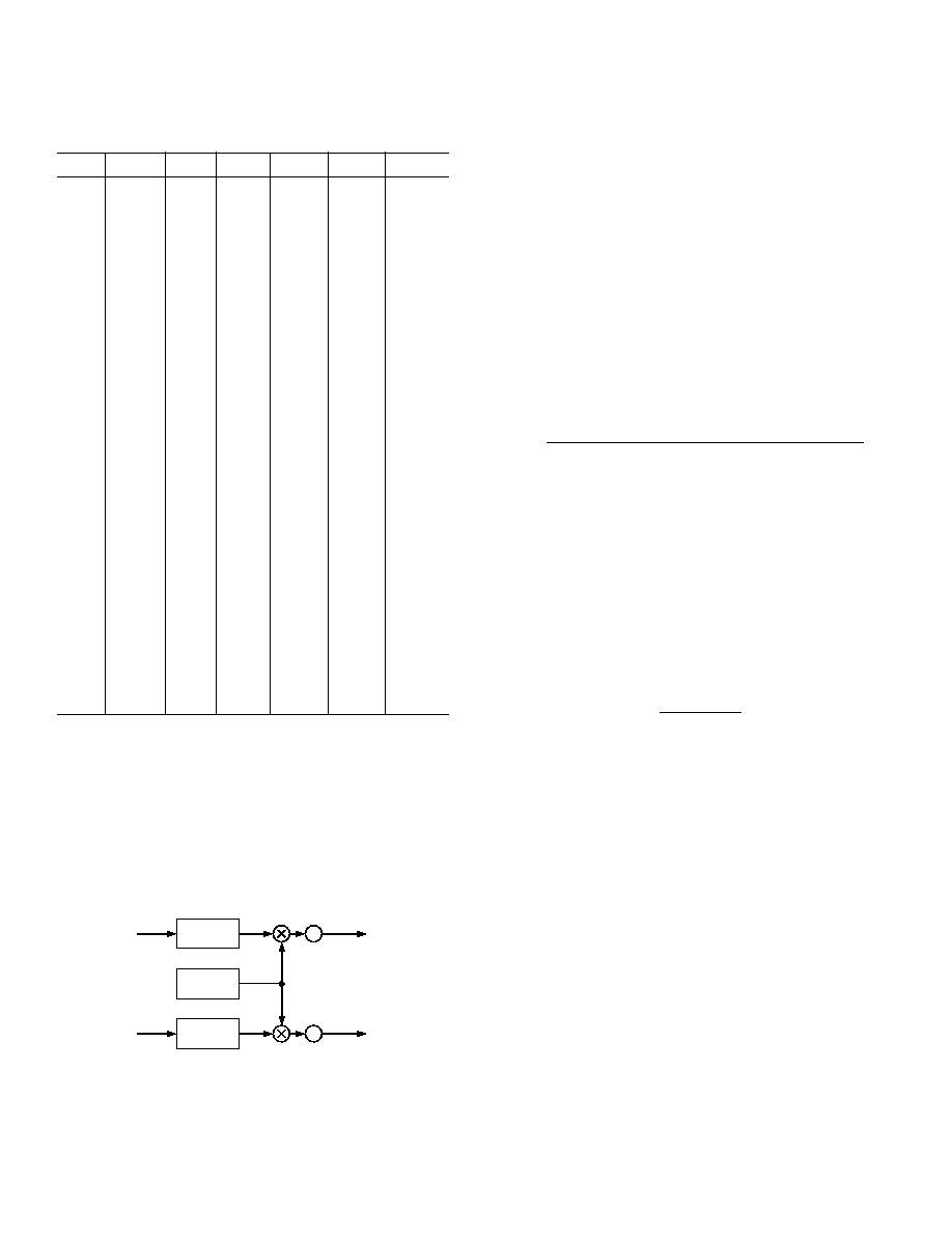
REV. 0
30
AD6635
Table IV. SSB CIC5 Alias Rejection Table (f
SAMP2
= 1).
Bandwidths are given as percentage of f
SAMP2
.
M
CIC5
50 dB 60 dB 70 dB 80 dB
90 dB 100 dB
2
10.227 8.078
6.393
5.066
4.008
3.183
3
7.924
6.367
5.110
4.107
3.297
2.642
4
6.213
5.022
4.057
3.271
2.636
2.121
5
5.068
4.107
3.326
2.687
2.170
1.748
6
4.267
3.463
2.808
2.270
1.836
1.480
7
3.680
2.989
2.425
1.962
1.588
1.281
8
3.233
2.627
2.133
1.726
1.397
1.128
9
2.881
2.342
1.902
1.540
1.247
1.007
10
2.598
2.113
1.716
1.390
1.125
0.909
11
2.365
1.924
1.563
1.266
1.025
0.828
12
2.170
1.765
1.435
1.162
0.941
0.760
13
2.005
1.631
1.326
1.074
0.870
0.703
14
1.863
1.516
1.232
0.998
0.809
0.653
15
1.740
1.416
1.151
0.932
0.755
0.610
16
1.632
1.328
1.079
0.874
0.708
0.572
17
1.536
1.250
1.016
0.823
0.667
0.539
18
1.451
1.181
0.960
0.778
0.630
0.509
19
1.375
1.119
0.910
0.737
0.597
0.483
20
1.307
1.064
0.865
0.701
0.568
0.459
21
1.245
1.013
0.824
0.667
0.541
0.437
22
1.188
0.967
0.786
0.637
0.516
0.417
23
1.137
0.925
0.752
0.610
0.494
0.399
24
1.090
0.887
0.721
0.584
0.474
0.383
25
1.046
0.852
0.692
0.561
0.455
0.367
26
1.006
0.819
0.666
0.540
0.437
0.353
27
0.969
0.789
0.641
0.520
0.421
0.340
28
0.934
0.761
0.618
0.501
0.406
0.328
29
0.902
0.734
0.597
0.484
0.392
0.317
30
0.872
0.710
0.577
0.468
0.379
0.306
31
0.844
0.687
0.559
0.453
0.367
0.297
32
0.818
0.666
0.541
0.439
0.355
0.287
RAM COEFFICIENT FILTER
The final signal processing stage for each individual channel is a
sum-of-products decimating filter with programmable coeffi-
cients. A simplified block diagram is shown below. The data
memories I-RAM and Q-RAM store the 160 most recent com-
plex samples from the previous filter stage with 20-bit resolution.
The coefficient memory, CMEM, stores up to 256 coefficients
with 20-bit resolution. On every CLK cycle, one tap for I and
one tap for Q are calculated using the same coefficients. The
RCF output consists of 24-bit data.
160 20B
I-RAM
IIN
IOUT
256 20B
C-RAM
160 20B
Q-RAM
QIN
QOUT
Figure 30. RAM Coefficient Filter (RCF) Block Diagram
RCF Decimation Register
Each RCF channel can be used to decimate the data rate. The
decimation register is an 8-bit register and can decimate from
1 to 256. The RCF decimation is stored in 0xA0 in the form of
MRCF 1. The input rate to the RCF is f
SAMP5
.
RCF Decimation Phase
The RCF decimation phase can be used to synchronize multiple
filters within a chip. This is useful when using multiple channels
within the AD6635 to implement a polyphase filter allowing the
resources of several RCF filters to be paralleled. In such an
application, two RCF filters would be processing the same data
from the CIC5. However, each filter will be delayed by one half
the decimation rate, thus creating a 180
phase difference between
the two halves.
The AD6635 filter channel uses the value stored in this register
to preload the RCF counter. Therefore, instead of starting from
0 (coefficient number 0), the counter is loaded with
Counter
decimation phase
Number of channels used
f
RCF decimationin each channel
f
CLK
RCF
=
¥
¥
¥
thus creating an offset in the processing that should be equiva-
lent to the required processing delay. The number of channels
or RCFs used to process one carrier is used in the above equa-
tion. f
CLK
is the input clock rate to the AD6635 and f
RCF
is the
input sample rate to the RCF from the CIC5 stage. This data is
stored in 0xA1 as an 8-bit number. The RCF decimation phase
can be used only when the ratio of RCF decimation and num-
ber of RCFs used is an integer.
RCF Filter Length
The maximum number of taps this filter can calculate, N
TAPS
, is
given by the equation below. The value N
TAPS
1 is written to
the Channel register within the AD6635 at address 0xA2.
N
f
M
f
TAPS
CLK
RCF
SAMP
£
¥
Ê
Ë
Á
^
¯
~
min
,
5
160
The function "min" used above gives the minimum of all the
expressions inside the parenthesis.
The RCF coefficients are located in addresses 0x00 to 0x7F and
are interpreted as 20-bit twos complement numbers. When
writing the coefficient RAM, the lower addresses will be multi-
plied by relatively older data from the CIC5 and the higher
coefficient addresses will be multiplied by relatively newer data
from the CIC5. The coefficients need not be symmetric and the
coefficient length, N
TAPS
, may be even or odd. If the coefficients
are symmetric, then both sides of the impulse response must be
written into the coefficient RAM.
Although the base memory for coefficients is only 128 words
long, the actual length is 256 words long. There are two pages,
each 128 words long. The page is selected by Bit 8 of 0xA4.

REV. 0
AD6635
31
Table VI. Output Mode Formats
Floating Point 12 + 4
1x
Floating Point 8 + 4
01
Fixed Point
00
Normally, the AD6635 will determine the exponent value that
optimizes numerical accuracy. However, if Bit 6 of this control
register is set, the values stored in Bits 30 is used to scale the
output. This ensures that consistent scaling and accuracy dur-
ing conditions that may warrant predictable output ranges. If
Bits 30 are represented by RCF Scale, then the scaling factor in
dB is given by:
Scaling Factor = RCF Scale 3
20
dB
10
(
)
¥
( )
log
2
For RCF Scale of 0, the Scaling Factor is equal to
18.06 dB, and for maximum RCF Scale of 15, the Scaling
Factor is equal to 72.25 dB.
If Bit 7 of this register is set, the same exponent will be used for
both the real and imaginary (I and Q) outputs. The exponent
used will be the one that prevents numeric overflow at the
expense of small signal accuracy. However, this is seldom a
problem, as small numbers would represent 0 regardless of
the exponent used.
Bit 8 of this register is the RCF bank select bit used to program
the register. When this bit is 0, the lowest block of 128 is selected
(taps 0 through 127). When high, the highest block is selected
(taps 128 through 255). It should be noted that while the chip
is computing filters, tap 127 is adjacent to 128 and there are no
paging issues.
Bit 9 of this register selects where the input to each RCF comes
from. If Bit 9 is clear, the RCF input comes from the CIC5
normally associated with the RCF. For Channels 0 through 3, if
the bit is set, the input comes from CIC5 Channel 1. The only
exception is Channel 1, which uses the output of CIC5 from
Channel 0 as its alternate. Using this feature, each RCF can
operate either on its own channel's NCO + rCIC2 + CIC5 data
or be paired with the RCF of Channel 1. The RCF of Channel 1
can also be paired with Channel 0. This control bit is used with
polyphase distributed filtering.
Similarly for Channels 4 through 7, if the bit is set, the input
comes from CIC5 Channel 5. The only exception is Channel 5,
which uses the output of CIC5 Channel 4 as its alternate source.
If Bit 10 is clear, the AD6635 channel operates in normal
mode. However, if Bit 10 is set, then the RCF is bypassed to
perform Channel BIST. See the Channel BIST (Built-in Self
Test) section below for more details.
Note that the outputs of the RCF can be sent directly to the
output ports (parallel or link) using the appropriate setting in
Port Control register (see Memory Map for Output Port Con-
trol Registers). Alternately, data from more than one channel
can be interleaved into the interpolating half-band filters and
AGCs (even if half-band filters and AGCs are bypassed, inter-
leaving function is still accomplished). This feature to interleave
data internal to the AD6635 allows the usage of multiple chan-
nels to process a single carrier.
Although this data must be written in pages, the internal core
handles filters that exceed the length of 128 taps. Therefore, the
full length of the data RAM may be used as the filter length
(160 taps). Though the RCF can calculate only 160 tap filters,
the filter coefficient memory is 256 words long so that more
than one filter configuration can be stored in the memory, and
can be selected using the Coefficient Offset 0xA3 register.
The RCF stores the data from the CIC5 into a 160
¥ 40 RAM.
160
¥ 20 is assigned to I data, and 160 ¥ 20 is assigned to Q
data. The RCF uses the RAM as a circular buffer so that it is
difficult to know in which address a particular data element is
stored. To avoid start-up transients due to undefined data RAM
values, the data RAM should be cleared upon initialization.
When the RCF is triggered to calculate a filter output, it starts
by multiplying the oldest value in the data RAM by the first
coefficient, which is pointed to by the RCF Coefficient Offset
register (0xA3). This value is accumulated with the products of
newer data-words multiplied by the subsequent locations in the
coefficient RAM until the coefficient address RCF
OFF
+ N
TAPS
1
is reached.
Table V. Three-Tap Filter
Coefficient Address
Impulse Response
Data
0
h(0)
N(0) oldest
1
h(1)
N(1)
2 = (N
TAPS
1)
h(2)
N(2) newest
The RCF Coefficient Offset register can be used for two pur-
poses. The main purpose of this register is allow for multiple
filters to be loaded into memory and selected simply by chang-
ing the offset as a pointer for rapid filter changes. The other use
of this register is to form part of symbol timing adjustment. If
the desired filter length is padded with zeros on the ends, the
starting point can be adjusted to form slight delays in when the
filter is computed with reference to the high speed clock. This
allows for vernier adjustment of the symbol timing. Course
adjustments can be made with the RCF Decimation Phase.
The output rate of this filter is determined by the output rate of
the CIC5 stage and M
RCF
:
f
f
M
SAMPR
SAMP
RCF
=
5
RCF Output Scale Factor and Control Register
Register 0xA4 is a compound register and is used to configure
several aspects of the RCF register. Bits 30 are used to set the
scale of the fixed-point output mode. This scale value may also
be used to set the floating-point outputs in conjunction with
Bit 6 of this register.
Bits 4 and 5 determine the output mode. Mode 00 sets the chip
up in fixed-point mode. The number of bits is determined by
the parallel or link port configuration.
Mode 01 selects floating-point mode 8 + 4. In this mode, an
8-bit mantissa is followed by a 4-bit exponent. In mode 1x (x
is don't care), the mode is 12 + 4, or 12-bit mantissa and 4-bit
exponent.
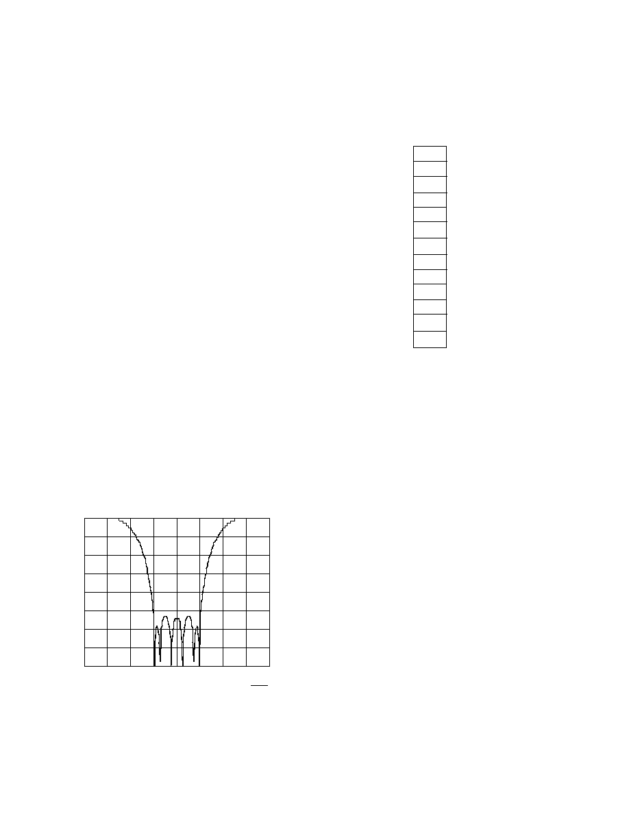
REV. 0
32
AD6635
INTERPOLATING HALF-BAND FILTERS
The AD6635 has four interpolating half-band FIR filters that
immediately precede the four digital AGCs and immediately
follow the RCF channel outputs. Each interpolating half-band
takes I and Q data from the preceding RCF and outputs I and
Q data to the AGC. The half-band filters and AGC operate
independently of each other, so the AGC can be bypassed, in
which case the output of the half-band filter is sent directly to
the output data port. The half-band filters also operate indepen-
dently of each otherany one can be enabled or disabled using
the Half-Band Control registers.
Half-band filters also perform the function of interleaving data
from various RCF channel outputs prior to the actual function
of interpolation. This interleaving of data is allowed even when
the actual function of the half-band filter is bypassed. This
feature allows for the usage of multiple channels (implementing
a polyphase filter) on the AD6635 to process a single carrier.
Either RCF phase decimation or a start holdoff counter for the
channels is used to appropriately phase the channels. For example,
if two channels of AD6635 are used to process one cdma2000
carrier, RCF filters for both channels should be 180
out of
phase. This can be done using RCF phase decimation or an
appropriate start holdoff counter followed by appropriate NCO
phase offsets.
Half-band filter A can listen to either Channels 0 to 3, Channels
0 and 1, or only Channel 0. Half-band filter B can listen to
Channels 2 and 3 or to only Channel 2. Each half-band filter
interleaves the channels specified in its control register. The
interleaved data so combined is interpolated by 2. The inter-
leaving function can be used independently of the interpolating
function, in which case the half-band filter is bypassed using the
Half-Band Control registers. When the half-band filter is bypassed,
the interleaving function is still performed. For one channel
running at twice the chip rate, the half-band can be used to
output channel data at 4
¥ the chip rate.
In Figure 31, the frequency response of the interpolating half-band
FIR filter is shown in the graph with respect to the chip rate.
FREQUENCY IN MULTIPLES OF CHIP RATE
0
0
1.0
2.0
3.0
3.5
4.0
AMPLITUDE dB
dB(INTERP(f))
20
40
60
70
80
0.5
1.5
2.5
10
30
50
f
SAMP
f
CHIP
Figure 31. Interpolating Half-Band Filter
Frequency Response
The SNR of the interpolating half-band filter is approximately
149.6 dB. The highest error spurs due to fixed-point arithmetic
are around 172.9 dB. The coefficients of the 13-tap interpolat-
ing half-band FIR filter are given in the Table VII.
Table VII. Half-Band Coefficients
0
14
0
66
0
309
512
309
0
66
0
14
0
AUTOMATIC GAIN CONTROL
The AD6635 is equipped with four independent automatic gain
control (AGC) loops for direct interface with a RAKE receiver.
Each AGC circuit has 96 dB of range. It is important that the
decimating filters of the AD6635 preceding the AGC reject
undesired signals so that each AGC loop is operating on only
the carrier of interest, and carriers at other frequencies do not
affect the ranging of the loop.
The AGC compresses the 23-bit complex output from the inter-
polating half-band filter into a programmable word size of 48,
10, 12, or 16 bits. Since the small signals from the lower bits are
pushed into higher bits by adding gain, the clipping of the lower
bits does not compromise the SNR of the signal of interest. The
AGC maintains a constant mean power on the output despite
the level of the signal of interest, allowing operation in environ-
ments where the dynamic range of the signal exceeds the
dynamic range of the output resolution.
The AGC and the interpolation filters are not tied together, and
any one or both of them can be selected without the other. The
AGC section can be bypassed if desired by setting Bit 0 of the
AGC control word. When bypassed, the I/Q data is passed to
the output port after clipping to 16-bit I/Q data.
There are three sources of error introduced by the AGC func-
tion: underflow, overflow, and modulation. Underflow is caused
by truncation of bits below the output range. Overflow is caused
by clipping errors when the output signal exceeds the output
range. Modulation error occurs when the output gain varies
during the reception of a data.
The desired signal level should be set based on the probability
density function of the signal so that the errors due to underflow
and overflow are balanced. The gain and damping values of the
loop filter should be set so that the AGC is fast enough to track
long term amplitude variations of the signal that might cause exces-
sive underflow or overflow, but slow enough to avoid excessive loss
of amplitude information due to the modulation of the signal.
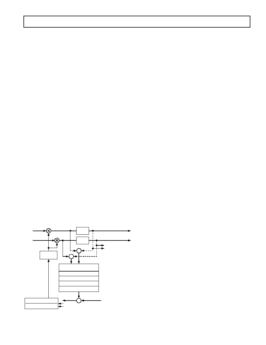
REV. 0
AD6635
33
The AGC Loop
The AGC loop is implemented using a log-linear architecture. It
contains four basic operations: power calculation, error calcula-
tion, loop filtering, and gain multiplication.
The AGC can be configured to operate in one of two modes:
Desired Signal Level mode or Desired Clipping Level mode, as
set by Bit 4 of AGC control word (0x0A, 0x12). The AGC adjusts
the gain of the incoming data according to how far it is from a
given desired signal level or desired clipping level, depending on
the mode of operation selected. Two data paths to the AGC
loop are provided: one before the clipping circuitry and one
after the clipping circuitry, as shown in Figure 32. For Desired
Signal Level mode, only the I/Q path from before the clipping is
used. For Desired Clipping Level mode, the difference of the I/Q
signals from before and after the clipping circuitry is used.
Desired Signal Level Mode
In this mode of operation, the AGC strives to maintain the
output signal at a programmable set level. This mode of operation
is selected by putting a value of zero in Bit 4 of AGC control
word (0x0A, 0x12). First, the loop finds the square (or power)
of the incoming complex data signal by squaring I and Q and
adding them. This operation is implemented in exponential
domain using 2x (power of 2).
The AGC loop has an average and decimate block. This average
and decimate operation takes place on power samples and before
the square root operation. This block can be programmed to
average 116384 power samples and the decimate section can
be programmed to update the AGC once every 14096 samples.
The limitation on the averaging operation is that the number of
averaged power samples should be a multiple of the decimation
value (1, 2, 3, or 4 times).
The averaging and decimation effectively means the AGC can
operate over averaged power of 116384 output samples. The
choice of updating the AGC once every 14096 samples and
operating on average power facilitates the implementation of a
loop filter with slow time constants, where the AGC error con-
verges slowly and makes infrequent gain adjustments. It would
also be useful in scenarios where the user wants to keep the gain
scaling constant over a frame of data (or a stream of symbols).
CLIP
I
23 BITS
Q
CLIP
MEAN SQUARE (I + jQ)
AVERAGE 116384 SAMPLES
DECIMATE 14096 SAMPLES
SQUARE ROOT
USED ONLY FOR
DESIRED
CLIPPING LEVEL
MODE
GAIN
MULTIPLIER
I
Q
2
X
POWER OF 2
Kz
1
1 (1 + P)z
1
+ Pz
2
ERROR
'K' GAIN
'P' POLE
+
'R' DESIRED
PROGRAMMABLE
BIT WIDTH
LOG
2
(X)
Figure 32. Block Diagram of the AGC
Due to the limitation on the number of average samples being a
multiple of the decimation value, only the multiple number 1, 2,
3, or 4 is programmed. This number is programmed in Bits 1, 0
of the 0x10 and 0x18 registers. These averaged samples are then
decimated with decimation ratios programmable from 1 to
4096. This decimation ratio is defined in the 12-bit registers
0x11 and 0x19.
The average and decimate operations are tied together and
implemented using a first-order CIC filter and some FIFO
registers. There is a gain and bit growth associated with CIC
filters, which depend on the decimation ratio. To compensate
for the gain associated with these operations, attenuation scaling
is provided before the CIC filter.
This scaling operation accounts for the division associated with
the averaging operation as well as the traditional bit growth in
CIC filters. Since this scaling is implemented as a bit shift
operation, only coarse scaling is possible. Fine scaling is imple-
mented as an offset in the Request Level explained later. The
attenuation scaling (SCIC) is programmable from 0 to 14 using
four bits of the 0x10 and 0x18 registers and is given by:
S
ceil
M
N
CIC
CIC
AVG
=
¥
(
)
[
]
log
2
where M
CIC
is the decimation ratio (14096) and N
AVG
is the
number of averaged samples programmed as a multiple of the
decimation ratio (1, 2, 3, or 4).
For example if a decimation ratio, M
CIC
, is 1000, and N
AVG
is
selected to be 3 (decimation of 1000 and averaging of 3000
samples), the actual gain due to averaging and decimation is
3000 or 69.54 dB (= 20 log 3000). Since attenuation is
implemented as a bit shift operation, only multiples of 6.02 dB
attenuations are possible. SCIC in this case is 12, corresponding
to 72.24 dB. This way SCIC scaling always attenuates more
than sufficiently to compensate for the gain changes in the aver-
age and decimate sections, and hence prevents overflows in the
AGC loop. But it is also evident that the CIC scaling is intro-
ducing a gain error (difference between gain due to CIC and
attenuation provided) of up to 6.02 dB. This error should be
compensated for in the Request signal level as explained below.
Logarithm to the base 2 is applied to the output from the aver-
age and decimate section. These decimated power samples (in
logarithmic domain) are converted to rms signal samples by
applying a square root. This square root is implemented using a
simple shift operation. The rms samples so obtained are sub-
tracted from the request signal level `R' specified in registers
(0x0B, 0x14) leaving an error term to be processed by the loop
filter, G(z).
The user sets this programmable request signal level `R' according
to the desired output signal level. The request signal level `R'
is programmable from 0 to 23.99 dB in steps of 0.094 dB. The
request signal level should also compensate for any error due to
the CIC scaling as explained previously. Hence, the request
signal level is offset by the amount of error induced in the CIC
given by
Offset
M
N
S
CIC
AVG
CIC
=
¥
(
)
¥
20
6 02
10
log
.
where, the offset is in dB.
Continuing with the previous example, this offset is given by
72.24 69.54 = 2.7 dB. So the request signal level is given by

REV. 0
34
AD6635
R
ceil
DSL
Offset
=
(
)
È
Î
Í
Í
°
¥
.
.
0 094
0 094
where R is the request signal level and DSL (desired signal
level) is the output signal level that the user desires. So, in the
previous example if the desired signal level is 13.8 dB, the
request level `R' is programmed to be 16.54 dB.
The AGC provides a programmable second order loop filter.
The programmable parameters, gain `K' and pole `P,' com-
pletely define the loop filter characteristics. The error term after
subtracting the request signal level is processed by the loop
filter, G(z). The open loop poles of the second-order loop filter
are 1 and `P,' respectively. The loop filter parameters, pole `P'
and gain `K,' allow adjustment of the filter time constant that
determines the window for calculating the peak-to-average ratio.
The open loop transfer function for the filter, including the gain
parameter is given by
G z
Kz
P z
Pz
( )
=
+
( )
+
1
1
2
1
1
If the AGC is properly configured (in terms of offset in Request
level), there are no gains except the filter gain K. Under these
circumstances a closed loop expression for the AGC loop is
possible, and is given by
G
z
G z
G z
Kz
K
P z
Pz
CLOSED
( )
=
( )
+
( )
=
+
(
)
+
1
1
1
1
1
2
The gain parameter `K,' and pole `P' are programmable through
registers (0x0E and 0x0F for AGC A and AGC C; 0x16 and
0x17 for AGC B and AGC D) from 0 to 0.996 in steps of
0.0039 using 8-bit representation. Though the user defines the
open loop pole `P' and gain `K,' they will directly impact the
placement of the closed loop poles and filter characteristics.
These closed loop poles P
1
and P
2
are the roots of the denomi-
nator in the above closed loop transfer function and are given by
P
P
K
P
K
P
1
2
1
1
4
2
,
P
2
=
+
(
)
+
+
(
)
Typically, the AGC loop performance is defined in terms of its
time constant or settling time. In such a case, the closed loop
poles should be set to meet the time constants required by the
AGC loop. The following relation between time constant and
closed loop poles can be used for this purpose.
P
M
Sample Rate
CIC
1
1
,
,
exp
2
2
=
¥
È
Î
Í
°
t
where
t
1,2
are the time constants corresponding to the poles
P
1, 2
. The time constants can also derived from settling times
as given below.
t =
2
5
%
%
settling time
4
settling time
3
or
M
CIC
(CIC decimation is from 1 to 4096) and either the settling
time or time constant should be chosen by the user. The sample
rate is the combined sample rate of all the interleaved channels
coming into the AGC/half-band interpolated filters. If two chan-
nels are being used to process one carrier of UMTS at 2 chip
rate, then each channel works at 3.84 MHz, and the combined
sample rate coming into the half-band interpolated filters is
7.68 MSPS. This rate should be used in the calculation of poles
in the above equation.
The loop filter output corresponds to the signal gain that is
updated by the AGC. Since all computation in the loop filter is
done in logarithmic domain (to the base 2) of the samples, the
signal gain is generated using the exponent (power of 2) of the
loop filter output.
The gain multiplier gives the product of the signal gain with both
the I and Q data entering the AGC section. This signal gain is
applied as a coarse 4-bit scaling and then a fine scale 8-bit
multiplier. Hence, the applied signal gain is between 48.16 dB
and +48.13 dB in steps of 0.024 dB. The initial value for
signal gain is programmable using the registers 0x0D and 0x15
for AGC A (AGC C) and AGC B (AGC D), respectively.
The products of the gain multiplier are the AGC scaled outputs
in 19-bit representation. These are in turn used as I and Q for
calculating the power and AGC error and loop filtered to pro-
duce signal gain for the next set of samples. These AGC scaled
outputs can be programmed as 4, 5, 6, 7, 8, 10, 12, or 16 bits
using the AGC control word (0x0A, 0x12). The AGC scaled
outputs are truncated to the required bit widths using the clip-
ping circuitry, as shown in the Functional Block Diagram.
Open Loop Gain Setting: If filter gain K occupies only 1 LSB
or 0.0039, then during the multiplication with the error term,
errors of up to 6.02 dB could be truncated. This truncation is
due to the lower bit widths available in the AGC loop. If filter
gain K were the maximum value, truncated errors would be a
less than 0.094 dB (equivalent to 1 LSB of error term represen-
tation). Generally, a small filter gain is used to achieve a large
time constant loop (or slow loops), but in this case, it would
cause large errors to go undetected. Due to this peculiarity, the
designers recommend that if a user wants slow AGC loops, they
should rather use fairly high values for filter gain K and then
use CIC decimation to achieve a slow loop. In this way, the
AGC loop will make large, infrequent gain changes compared
to small and frequent gain changes, as in the case of a normal
small gain loop filter. However, though the AGC loop makes
large, infrequent gain changes, a slow time constant is still
achieved and there is less truncation of errors.
Average Samples Setting: Though it is complicated to express
the exact effect of the number of averaging samples, thinking
intuitively, it has a smoothing effect on the way the AGC loop
attacks a sudden increase or a spike in the signal level. If averag-
ing of four samples is used, the AGC will attack a sudden
increase in signal level more slowly compared to no averaging.
The same would apply to the manner in which the AGC would
attack a sudden decrease in the signal level.
Desired Clipping Level Mode
As noted previously, each AGC can be configured so that the
loop locks on to a desired clipping level or a desired signal level.
The Desired Clipping Level mode can be selected by setting
Bit 4 of the individual AGC control words (0x0A, 0x12). For
signals that tend to exceed the bounds of the peak-to-average
ratio, desired clipping level option offers a way to keep from
truncating those signals and still provides an AGC that attacks
quickly and settles to the desired output level. The signal path
for this mode of operation is shown with the dashed arrows in

REV. 0
AD6635
35
Figure 32 (Block Diagram of the AGC), and the operation is
similar to the Desired Signal Level mode.
First, the data from the gain multiplier is truncated to a lower
resolution (4, 5, 6, 7, 8, 10, 12, or 16 bits) as set by the AGC
control word. An error term (both I and Q) is generated that is
the difference between the signals before and after truncation.
This term is passed to the complex squared magnitude block for
averaging and decimating the update samples and taking their
square root to find rms samples, just as in Desired Signal
Level mode. In place of the request desired signal level, a
desired clipping level is subtracted, leaving an error term to be
processed by the second-order loop filter. The rest of the loop
operates the same way as the Desired Signal Level mode. This
way the truncation error is calculated and the AGC loop oper-
ates to maintain a constant truncation error level.
Apart from Bit 4 of the AGC control words, the only other
register setting change, compared to the Desired Signal Level
mode, is that the Desired Clipping level is stored in the AGC
Desired Level registers (0x0C, 0x15) instead of the Request
Signal Level (as in Desired Signal Level mode).
Synchronization
In scenarios where AGC output is connected to a RAKE receiver,
the RAKE receiver can synchronize the average and update sec-
tion to update the average power for AGC error calculation and
loop filtering. This external sync signal synchronizes the AGC
changes to the RAKE receiver and makes sure that the AGC
gain does not change over a symbol period, resulting in more
accurate estimation. Such synchronization can be accomplished
by setting the appropriate bits of the AGC control register.
When the channel comes out of sleep, it loads the AGC holdoff
counter value and starts counting down, clocked by the Master
clock. When this counter reaches zero, the CIC filter of the
AGC starts decimation and updates the AGC loop filter based
on the set CIC decimation value.
Further, whenever the user wants to synchronize the start of
decimation for a new update sample, an appropriate holdoff
value can be set in the AGC Holdoff counter (0x0B, 0x13) and
then the Sync now bit (Bit 3) in the AGC control word is set.
Upon setting this bit, the holdoff counter value is counted down
and a CIC decimated value is updated on the count of zero.
Along with updating a new value, the CIC filter accumulator
can be reset if Init on Sync bit (Bit 2) of the AGC control word
is set. Each sync will initiate a new sync signal unless first sync
only bit (Bit 1) of the AGC control word is set. If this bit is not
set, again the holdoff counter is loaded with the value in the
Holdoff register to count down and repeat the same process.
These additional features make the AGC synchronization more
flexible and applicable to varied circumstances.
Addresses 0x0A0x11 have been reserved for configuring AGC
A, and addresses 0x120x19 have been reserved for configuring
AGC B. The register specifications are detailed in the Memory
Map for Output Port Control Registers section.
USER-CONFIGURABLE BUILT-IN SELF TEST (BIST)
The AD6635 includes two built-in test features to test the integ-
rity of each channel. The first is a RAM BIST and is intended
to test the integrity of the high speed random access memory
within the AD6635. The second is Channel BIST, which is
designed to test the integrity of the main signal paths of the
AD6635. Each BIST function is independent of the other,
meaning that each channel can be tested independently at the
same time.
RAM BIST
The RAM BIST can be used to validate functionality of the
on-chip RAM. This feature provides a simple pass/fail test,
which will give confidence that the channel RAM is operational.
The following steps should be followed to perform this test.
1. The channels to be tested should be put into Sleep mode via
the external address register 0x011.
2. The RAM BIST Enable bit in the RCF register 0xA8
should be set high.
3. Wait 1600 clock cycles.
4. Register 0xA8 should be read back. If Bit 0 is high, the test
is not yet complete. If Bit 0 is low, the test is complete and
Bits 1 and 2 indicate the condition of the internal ram. If
Bit 1 is high, then CMEM is bad. If Bit 2 is high, then
DMEM is bad.
Table VIII. BIST Register 0xA8
0xA8
Coefficient MEM
Data MEM
XX1
Test incomplete
Test incomplete
000
PASS
PASS
010
FAIL
PASS
100
PASS
FAIL
110
FAIL
FAIL
Channel BIST
The Channel BIST is a thorough test of the selected AD6635
signal path. With this test mode, it is possible to use externally
supplied vectors or an internal pseudorandom generator. An
error signature register in the RCF monitors the output data of
the channel, and is used to determine whether the proper data
exits the RCF. If errors are detected, each internal block may be
bypassed and another test can be run to debug the fault. The I
and Q paths are tested independently. The following steps
should be followed to perform this test.
1. The channels to be tested should be configured as required
for the application, setting the decimation rates, scalars,
and RCF coefficients.
2. The channels should remain in the Sleep mode.
3. The Start Holdoff counter of the channels to be tested
should be set to 1.
4. Memory locations 0xA5 and 0xA6 should be set to 0.
5. The Channel BIST located at 0xA7 should be enabled by
setting Bits 190 to the number of RCF outputs to observe.
6. Bit 4 of External Address Register 5 should be set high to
start the soft sync.
7. Set the SYNC bits high for the channels to be tested.
8. Bit 6 must be set to 0 to allow the user to provide test
vectors. The internal pseudorandom number generator
may also be used to generate an input sequence by setting
Bit 7 high.
9. An internal full-scale sine wave can be inserted when Bit 6
is set to 1 and Bit 7 is cleared.
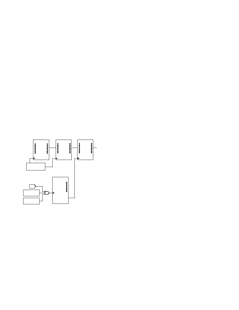
REV. 0
36
AD6635
10. When the SOFT_SYNC is addressed, the selected channels
will come out of the sleep mode and processing will occur.
11. If the user is providing external vectors, then the chip may
be brought out of Sleep mode by one of the other methods,
provided that either of the IEN inputs is inactive until the
channel is ready to accept data.
12. After a sufficient amount of time, the Channel BIST Signa-
ture registers 0xA5 and 0xA6 will contain a numeric value
that can be compared to the expected value for a known
good AD6635 with the exact same configuration. If the
values are the same, then there is a very low probability that
there is an error in the channel.
CHIP SYNCHRONIZATION
Two types of synchronization can be achieved with the
AD6635. These are Start and Hop. Each is described in detail
below. The synchronization is accomplished with the use of a
shadow register and a holdoff counter. See Figure 33 for a
simplified schematic of the NCO shadow register and NCO
Frequency Holdoff counter to understand its basic operation.
Enabling the clock (AD6635 CLK) for the holdoff counter can
occur with either a Soft_Sync (via the Microport) or a pin sync
(via any of the four AD6635 SYNC Pins A, B, C, or D).
I0
I31
Q0
Q31
MICRO
REGISTER
I0
I31
Q0
Q31
SHADOW
REGISTER
I0
I31
Q0
Q31
NCO
FREQUENCY
REGISTER
FROM
MICROPORT
B0
B15
NCO FREQUENCY
UPDATE HOLD OFF
COUNTER
TC
ENB
TO
NCO
SOFT SYNC
ENABLE
AD6635
CLK
PIN SYNC
ENABLE
Figure 33. NCO Shadow Register and Holdoff Counter
The four SYNC pins available on the AD6635 are common to
the entire chip, i.e., all 8 channels and all 4 AGCs. On the other
hand, the 4 Soft Sync channels specific to Channels 0 to 3 and
AGCs A and B are different from the 4 Soft Sync channels
specific to Channels 4 to 7 and AGCs C and D. This is the
effect of using different chip selects (
CS0 and CS1) for these
different sets of sync channels. When using
CS1 to program the
microport, the SOFT_SYNC register (external address 0x5)
and the SOFT SYNCs for Channels 4, 5, 6, and 7 are pro-
grammed. It should be noted that the SYNC pins are separate
from SOFT_SYNC Channels 0, 1, 2, and 3.
Start
Start refers to the startup of an individual channel, chip, or
multiple chips. If a channel is not used, it should be put in the
Sleep mode to reduce power dissipation. Following a hard reset
(low pulse on the AD6635
RESET pin), all channels are
placed into Sleep mode. Channels may also be manually put to
sleep by writing to the external address 0x3 controlling the
sleep function.
Start with No Sync
If no synchronization is needed to start multiple channels or
multiple AD6635s, the following method should be used to
initialize the device:
1. To program a channel, it must first be set to Sleep mode (bit
high, Ext address 3). All appropriate control and memory
registers (filter) are then loaded. The Start Update Holdoff
counter (0x83) should be set to 1:
2. Set the Sleep bits low (Ext address 3). This enables the chan-
nel. Note that when using external addresses, appropriate
chip selects should be used for the different channels. Chan-
nels 03 are started when
CS0 is used, and Channels 4 7
when
CS1 is used.
Start with Soft Sync
The AD6635 includes the ability to synchronize channels or
chips under microprocessor control. One action to synchronize
is the start of channels or chips. The Start Update Holdoff
counter (0x83) in conjunction with the Start bit and Sync bit
(Ext address 5) allow this synchronization. Basically, the Start
Update Holdoff counter delays the start of a channel(s) by its
value (number of AD6635 CLKs). The following method is
used to synchronize the start of multiple channels via micropro-
cessor control:
1. Set the appropriate channels to Sleep mode (a hard reset to
the AD6635
RESET pin brings all four channels up in
Sleep mode).
2. Note that the time from when the RDY (
DTACK) pin goes
high to when the NCO begins processing data is the contents
of the Start Update Holdoff Counter(s) (0x83) plus six mas-
ter clock cycles.
3. Write the Start Update Holdoff counter(s) (0x83) to the
appropriate value (greater than 1 and less than 216 1). If
the chip(s) is not initialized, all other registers should be
loaded at this step.
4. Write the Start bit and the SYNC bit high (Ext address 5).
5. This starts the Start Update Holdoff counter counting
down. The counter is clocked with the AD6635 CLK signal.
When it reaches a count of one, the Sleep bit of the appropri-
ate channel(s) is set low to activate the channel(s).
6. Note that Channels 0 to 3 and 4 to 7 will receive syncs
during different microport writes (separate syncs have to be
used for Channels 0 to 3 and 4 to 7). This time difference
for the two sets of channels (separate microport writes)
should be noted.
Start with Pin Sync
The AD6635 has four Sync Pins, A, B, C, and D, that can
provide for very accurate synchronization channels. Each chan-
nel can be programmed to listen to any of the four Sync pins.
Additionally, any or all channels can monitor a single Sync pin
or each can monitor a separate pin, providing complete flexibil-
ity in synchronization. Synchronization of Start with one of the
external signal is accomplished with the following method.

REV. 0
AD6635
37
1. Set the appropriate channels to Sleep mode (a hard reset to
the AD6635
RESET pin brings all four channels up in sleep
mode).
2. Note that the time from when the Sync pin goes high to
when the NCO begins processing data is the contents of the
Start Update Holdoff counter(s) (0x83) plus three master
clock cycles.
3. Write the Start Update Holdoff counter(s) (0x83) to the
appropriate value (greater than 1 and less than 216 1). If
the chip(s) is not initialized, all other registers should be
loaded at this step.
4. Set the Start on Pin Sync bit and the appropriate Sync Pin
Enable high (Ext address 4; A, B, C, or D).
5. When the Sync pin is sampled high by the AD6635 CLK,
this enables the countdown of the Start Update Holdoff
counter. The counter is clocked with the AD6635 CLK
signal. When it reaches a count of one, the Sleep bit of the
appropriate channel(s) is set low to activate the channel(s).
6. Unlike Soft Syncs, Pin Syncs have effect on all the channels at
the same time. See Step 6 of the previous section, Start with
Soft Sync to understand the delays between the two sets of
channels. These delays do not occur with Pin Sync since the
Sync pins are shared between all the AD6635 channels.
Hop
Hop is a jump from one NCO frequency to a new NCO fre-
quency. This change in frequency can be synchronized via
microprocessor control (Soft Sync) or an external Sync signal
(Pin Sync) as described below.
To set the NCO frequency without synchronization, the follow-
ing method should be used.
Set Frequency No Hop
1. Set the NCO Freq Holdoff counter to 0.
2. Load the appropriate NCO frequency. The new frequency
will be immediately loaded to the NCO.
Hop with Soft Sync
The AD6635 includes the ability to synchronize a change in
NCO frequency on multiple channels or chips under micropro-
cessor control. The NCO Freq Holdoff counter (0x84) in
conjunction with the Hop bit and the Sync bit (Ext address 4)
allow this synchronization. Basically, the NCO Freq Holdoff
counter delays the new frequency being loaded into the NCO
by its value (number of AD6635 CLKs). The following method
is used to synchronize a hop in frequency on multiple channels
via microprocessor control.
1. Note that the time from when the RDY (
DTACK) pin goes
high to when the NCO begins processing data is the contents
of the NCO Freq Holdoff counter (0x84) plus seven master
clock cycles.
2. Write the NCO Freq Hold Off (0x84) counter to the appro-
priate value (greater than 1 and less than 216 1).
3. Write the NCO Frequency register(s) to the new desired
frequency.
4. Write the Hop bit and the Sync(s) bit high (Ext address 4).
5. This starts the NCO Freq Holdoff counter counting down.
The counter is clocked with the AD6635 CLK signal. When
it reaches a count of one, the new frequency is loaded into
the NCO.
6. Note that channels 0 to 3 and 4 to 7 will receive syncs during
different microport writes (separate syncs have to be used for
Channels 0 to 3 and 4 to 7). This time difference for the two
sets of channels (separate microport writes) should be noted.
Hop with Pin Sync
The AD6635 includes four Sync pins to provide the most accu-
rate synchronization, especially between multiple AD6635s.
Synchronization of hopping to a new NCO frequency with an
external signal is accomplished with the following method.
1. Note that the time from when the SYNC pin goes high to
when the NCO begins processing data is the contents of the
NCO Freq Holdoff counter (0x84) plus five master clock
cycles.
2. Write the NCO Freq Holdoff counter(s) (0x84) to the
appropriate value (greater than 1 and less than 216 1).
3. Write the NCO Frequency register(s) to the new desired
frequency.
4. Set the Hop on Pin Sync bit and the appropriate Sync Pin
Enable high.
5. When the selected Sync pin is sampled high by the AD6635
CLK, this enables the countdown of the NCO Freq Holdoff
counter. The counter is clocked with the AD6635 CLK
signal. When it reaches a count of one, the new frequency is
loaded into the NCO.
6. Unlike Soft Syncs, Pin Syncs have effect on all the channels
at the same time. See Step 6 of the section, Start with Soft
Sync, to understand the delays between the two sets of chan-
nels. These delays do not occur with Pin Sync since all the
Sync pins are shared between all the AD6635 channels.
PARALLEL OUTPUT PORTS
The AD6635 incorporates four independent 16-bit parallel
ports and link ports for output data transfer. The parallel ports
and link ports share pins and internal mux circuitry. For each
data path, i.e., for each Output Port (A, B, C, or D), either a
parallel port or a link port can be selected, but not both. A
parallel port and a link port can be used simultaneously, but
only if they do not share the same data path; for example, Paral-
lel Port A along with Link Port B, or Parallel Port B with Link
Port A. Figure 34 illustrates a simplified block diagram showing
the AD6635's output data routing configuration for one output
port. It also shows the shared pins; eight pins of AD6635 are
shared with link port data pins and the parallel port channel
indicator pins are shared with the link port clock in and clock
out pins.
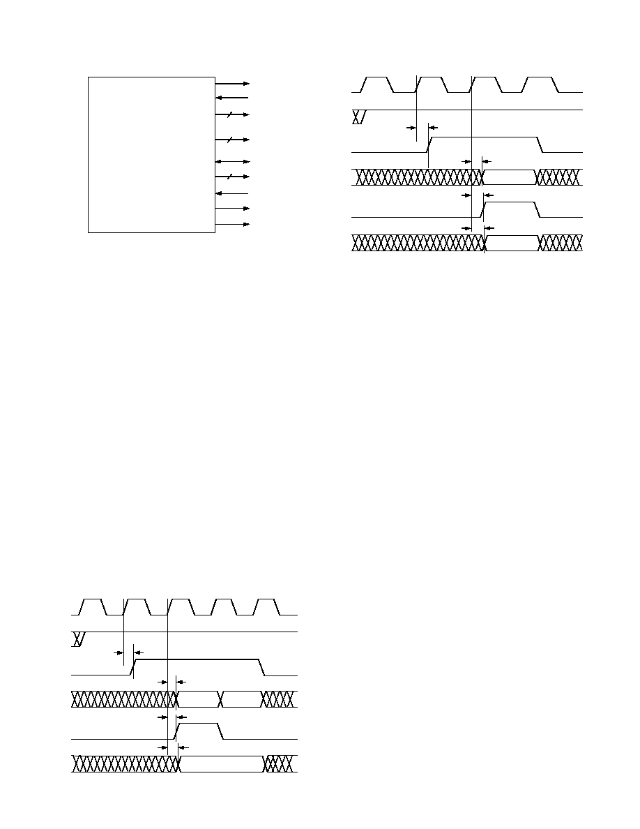
REV. 0
38
AD6635
LINK PORT A CLOCK OUT
LINK PORT A CLOCK IN
2
LINK PORT A DATA
OR 8 LSBs OF
PARALLEL PORT A
DATA (SHARED PINS)
PCLKO
PARALLEL PORT A
MSB DATA
PARALLEL PORT A ACK
PARALLEL PORT A REQ
PARALLEL PORT A
I AND Q INDICATOR
PORT A
AD6635
ABOVE PINS SHARED
WITH PARALLEL PORT A
CHANNEL INDICATOR
8
8
Figure 34. Data Routing for Output Port A
Parallel port configuration is specified by accessing Port Control
register addresses 0x1A and 0x1C. Port clock Master/Slave
mode (described later) is configured using the Port Clock Con-
trol register at address 0x1E. It should be noted that Output
Ports A and B have a separate clock (PCLK0) from Output
Ports C and D (PCLK1). Note that to access these registers,
Bit 5 (Access Port Control registers) of external address 3
(SLEEP register) must be set. The address is then selected by
programming the CAR register at external address 6.
The parallel ports are enabled by setting Bit 7 of the Link Con-
trol registers at addresses 0x1B and 0x1D.
Each parallel port is capable of operating in either Channel
mode or AGC mode. Each mode is described in detail below.
Channel Mode
Parallel port Channel mode is selected by setting Bit 0 of addresses
0x1A and 0x1B. In Channel mode, I and Q words from each
channel are directed to the parallel port, bypassing the interleaver,
the interpolating half-band filter, and AGC. The specific chan-
nels output by the port are selected by setting Bits 14 of the
Input Port Control register 0x1A and 0x1C. Each Channel
03 can be independently output on either Port A, Port B, or
both. Similarly, each Channel 47 can be independently output
on either Port C, Port D, or both.
Channel mode provides two data formats. Each format requires
a different number of parallel port clock (PCLK) cycles to com-
plete the transfer of data. In each case, each data element is
transferred during one PCLK cycle. See Figures 35 and 36,
which present Channel mode parallel port timing.
t
DPCH
t
DPIQ
t
DPP
PCLKn
PxACK
PxREQ
t
DPREQ
Px[15:0]
I[15:0]
Q[15:0]
PxlQ
PxCH[1:0]
PxCH[1:0] = CHANNEL NO.
Figure 35. Channel Mode Interleaved Format (16-bit I/Q)
t
DPREQ
t
DPCH
t
DPIQ
t
DPP
PCLKn
PxREQ
PxlQ
PxCH[1:0]
PxCH[1:0] =
CHANNEL NO.
Px[15:0]
I[15:8]; Q[7:0]
PxACK
Figure 36. Channel Mode 8I/8Q Parallel Format
The 16-bit interleaved format provides I and Q data for each
output sample on back-to-back PCLK cycles. Both I and Q
words consist of the full port width of 16 bits. Data output is
triggered on the rising edge of PCLK when both REQ and ACK
are asserted. I data is output during the first PCLK cycle, and
the PxIQ output indicator pins are set high to indicate that I
data is on the bus. Q data is output during the subsequent
PCLK cycle, and the PxIQ output indicator pins are low during
this cycle.
The 8-bit concurrent format provides 8 bits of I data and 8 bits
of Q data simultaneously during one PCLK cycle, also triggered
on the rising edge of PCLK. The I byte occupies the most sig-
nificant byte of the port, while the Q byte occupies the least
significant byte. The PxIQ (where x = A, B, C, or D) output
indicator pins are set high during the PCLK cycle. Note that if
data from multiple channels are output consecutively, the PxIQ
output indicator pins will remain high until data from all chan-
nels has been output. It should be noted that output Ports
(either parallel or link) A and B can output data only from
Channels 03, and similarly, Output Ports C and D can output
data only from Channels 47.
The PACH[1:0] and PBCH[1:0] pins provide a 2-bit binary
value indicating the source channel of the data currently being
output. This value will convey the channel numbers 0 to 3.
Similarly PCCH[1:0] and PDCH[1:0] pins provide a 2-bit
binary value indicating the source channel of the data currently
being output, the channels being 4 to 7. Binary value 00 indi-
cates Channel 4, and value 11 indicates Channel 7.
Care should be taken to read data from the port as soon as
possible. If not, the sample will be overwritten when the next
new data sample arrives. This occurs on a per channel basis;
i.e., a Channel 0 sample will only be overwritten by a new
Channel 0 sample, and so on.
The order of data output is dependent on when data arrived at
the port, which is a function of total decimation rate, Start
Holdoff values, and so on. Priority order is, from highest to
lowest, Channels 0, 1, 2, and 3, and similarly on Ports C and D
it is Channels 4, 5, 6, and 7.
AGC Mode
Parallel port channel mode is selected by clearing Bit 0 of
addresses 0x1A and 0x1C. I and Q data output in AGC mode
are output from the AGC, not the individual channels. Parallel
Ports A and B can provide data from either AGC A, AGC B, or
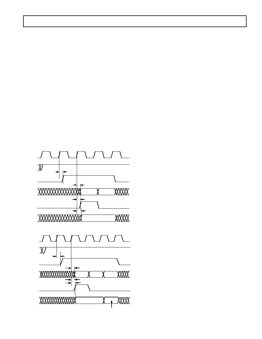
REV. 0
AD6635
39
both. Bits 1 and 2 of register addresses 0x1A and 0x1C control
the inclusion of data from AGCs A and B, respectively. Simi-
larly, Parallel Ports C and D can provide data from either
AGC C, AGC D, or both.
AGC mode provides only one I and Q format, which is similar
to the 16-bit Interleaved format of Channel mode. When both
REQ and ACK are asserted, the next rising edge of PCLK
triggers the output of a 16-bit AGC I word for one PCLK cycle.
The PxIQ (x = A, B, C, or D) output indicator pins are high
during this cycle, and low otherwise. A 16-bit AGC Q word is
provided during the subsequent PCLK cycle. If the AGC gain
word has been updated since the last sample, a 12-bit RSSI
word (Receive Signal Strength Indicator) is provided during the
PCLK cycle following the Q word on the 12 MSBs of the paral-
lel port data pins. The RSSI word is the bit inverse of the signal
gain word used in the gain multiplier of the AGC.
The data provided by the PACH[1:0] and PBCH[1:0] pins in
AGC mode is different than that provided in Channel mode. In
AGC mode, PACH[0] and PBCH[0] indicate the AGC source
of the data currently being output (0 = AGC A, 1 = AGC B).
PACH[1] and PBCH[1] indicate whether the current data is an
I/Q word or an AGC RSSI word (0 = I/Q word, 1 = AGC RSSI
word). The two different AGC outputs are shown in Figures 37
and 38.
I[15:0]
Q[15:0]
PxCH[0] = AGC NO.
PxCH[1] = 0
t
DPCH
t
DPP
PCLKn
PxREQ
Px[15:0]
PxACK
PxlQ
PxCH[1:0]
t
DPIQ
t
DPREQ
Figure 37. AGC with No RSSI Word
PxCH[0] = AGC NO.
PxCH[1] = 0
PxCH[0] = AGC NO.
PxCH[1] = 1
t
DPP
PCLKn
PxREQ
Px[15:0]
PxACK
PxlQ
PxCH[1:0]
I[15:0]
Q[15:0]
RSSI[11:0]
t
DPREQ
t
DPIQ
t
DPCH
Figure 38. AGC with RSSI Word
Master/Slave PCLKn Modes
The parallel ports may operate in either Master or Slave mode.
The mode is set via the Port Clock Control register (address
0x1E). The parallel ports power up in Slave mode to avoid
possible contentions on the PCLKn pin. Parallel Ports A and B
can be set up in Master mode while Ports C and D are set up in
Slave mode, or vice versa. But, both the Ports A and B, or C
and D, should be in the same mode, since they share the paral-
lel port clock PCLK0 and PCLK1, respectively.
In Master mode, PCLK is an output whose frequency is the
AD6635 clock frequency divided by the PCLK divisor. Since
values for PCLK_divisor [2:1] can be set to 0, 1, 2, or 3, integer
divisors of 1, 2, 4, or 8, respectively, can be obtained. Since the
maximum clock rate of the AD6635 is 80 MHz, the highest
PLCK rate in Master mode is also 80 MHz. Master mode is
selected by setting Bit 0 of address 0x1E.
In Slave mode, external circuitry provides the PCLK signal.
Slave mode PCLK signals may be either synchronous or
asynchronous. The maximum Slave mode PCLK frequency
is 100 MHz.
Parallel Port Pin Functionality
The following describes the functionality of the pins used by the
parallel ports.
PCLK: Input/output. As an output (Master mode), the maxi-
mum frequency is CLK/N, where CLK is the AD6635 clock
and N is an integer divisor of 1, 2, 4, or 8. As an input (Slave
mode), it may be asynchronous relative to the AD6635 CLK.
This pin powers up as an input to avoid possible contentions.
Other port outputs change on the rising edge of PCLK.
REQ: Active high output, synchronous to PCLK. A logic high
on this pin indicates that data is available to be shifted out of
the port. The logic level remains high until all pending data has
been shifted out.
ACK: Active high asynchronous input. Applying a logic low on
this pin inhibits parallel port data shifting. Applying a logic high
to this pin when REQ is high causes the parallel port to shift out
data according to the programmed data mode. ACK is sampled
on the rising edge of PCLK. Assuming REQ is asserted, the
latency from the assertion of ACK to data appearing at the
parallel port output is no more than 1.5 PCLK cycles (see
Figure 12). ACK may be held high continuously; in this case,
when data becomes available, shifting begins one PCLK cycle
after the assertion of REQ (see Figures 35, 36, and 37).
PAIQ, PBIQ, PCIQ, PDIQ: High whenever I data is present
on the port output, low otherwise.
PxCH[1:0], PxCH[1:0], PCCH[1:0], PDCH[1:0]: These pins
serve to identify data in both of the data modes. In Channel
mode, these pins form a 2-bit binary number identifying the
source channel of the current data word. In AGC mode, [0]
indicates the AGC source (0 = AGC A, 1 = AGC B), and [1]
indicates whether the current data word is (0 = I/Q data) or
(1 = RSSI word). Similarly for parallel Ports C and D, [0]
indicates the AGC source (0 = AGC C, 1 = AGC D), and [1]
indicates whether the current data word is (0 = I/Q data) or
(1 = RSSI word).
PA[15:0], PB[15:0], PC[15:0], PD[15:0]: Parallel output data
ports. Contents and format are mode dependent.
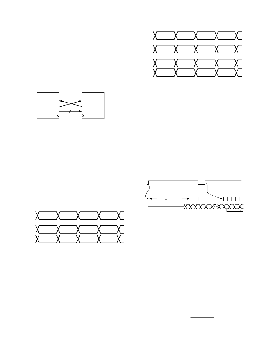
REV. 0
40
AD6635
LINK PORT
The AD6635 has four configurable link ports that provide a
seamless data interface with the TigerSHARC DSP. Each link
port allows the AD6635 to write output data to the receive
DMA channel in the TigerSHARC for transfer to memory.
Since they operate independently of each other, each link port
can be connected to a different TigerSHARC or to different link
ports on the same TigerSHARC. Figure 39 shows how to con-
nect one of the four AD6635 link ports to one of the four
TigerSHARC link ports. Individual link ports are configured
through their respective registers.
AD6635
LCLKIN
LCLKOUT
LDAT
PCLK
TigerSHARC
LCLKIN
LCLKOUT
LDAT
PCLK
8
Figure 39. Link Port Connection between AD6635
and TigerSHARC
Link Port Data Format
Each link port can output data to the TigerSHARC in five
different formats: 2-channel, 4-channel, dedicated AGC,
redundant AGC with RSSI word, and redundant AGC without
RSSI word. Each format outputs 2 bytes of I data and 2 bytes of
Q data to form a 4-byte IQ pair. Since the TigerSHARC link
port transfers data in quad-word (16-byte) blocks, four IQ pairs
can make up one quad-word. If the channel data is selected (Bit
0 of 0x1B/0x1D = 0), then 4-byte IQ words of the four channels
can be output in succession, or alternating channel pair IQ
words can be output. Figures 40 and 41 show the quad-word
transmitted for each scenario with corresponding register values
for configuring each link port.
LINK PORT
A OR B
CH 0 I, Q
(4 BYTES)
CH 1 I, Q
(4 BYTES)
CH 2 I, Q
(4 BYTES)
CH 3 I, Q
(4 BYTES)
ADDR 0x1B OR 0x1D BIT 0 = 0, BIT 1 = 0
LINK PORT A
CH 0 I, Q
(4 BYTES)
CH 1 I, Q
(4 BYTES)
CH 0 I, Q
(4 BYTES)
CH 1 I, Q
(4 BYTES)
LINK PORT B
CH 2 I, Q
(4 BYTES)
CH 3 I, Q
(4 BYTES)
CH 2 I, Q
(4 BYTES)
CH 3 I, Q
(4 BYTES)
ADDR 0x1B OR 0x1D BIT 0 = 0, BIT 1 = 1
Figure 40. Link Port Data from RCF
If AGC output is selected (Bit 0 of 0x1B/0x1D = 1), then RSSI
information can be sent with the IQ pair from each AGC. Each
link port can be configured to output data from one AGC or
both link ports can output data from the same AGC. If both link
ports are transmitting the same data, then RSSI information
must be sent with the IQ words (Bit 2 = 0). Note that the actual
AGC RSSI is only 2 bytes (12 bits of RSSI word appended with
four zeros), so the link port sends 2 bytes of 0s immediately after
each RSSI word to make a full 16-byte quad-word.
LINK PORT
A OR B
AGC A I, Q
(4 BYTES)
AGC B I, Q
(4 BYTES)
AGC A I, Q
(4 BYTES)
AGC B I, Q
(4 BYTES)
ADDR 0x1B OR 0x1D BIT 0 = 1, BIT 1 = 0, BIT 2 = 0
LINK PORT
A OR B
AGC A I, Q
(4 BYTES)
AGC A RSSI
(4 BYTES)
AGC B I, Q
(4 BYTES)
AGC B RSSI
(4 BYTES)
ADDR 0x1B OR 0x1D BIT 0 = 1, BIT 1 = 0, BIT 2 = 1
LINK PORT A
AGC A I, Q
(4 BYTES)
AGC A RSSI
(4 BYTES)
AGC A I, Q
(4 BYTES)
AGC A RSSI
(4 BYTES)
AGC B I, Q
(4 BYTES)
AGC B RSSI
(4 BYTES)
AGC B I, Q
(4 BYTES)
AGC B RSSI
(4 BYTES)
LINK PORT B
ADDR 0x1B OR 0x1D BIT 0 = 1, BIT 1 = 1, BIT 2 = 0
Figure 41. Link Port Data from AGC
Note that Bit 0 = 1, Bit 1 = 0, and Bit 2 = 1 is not a valid con-
figuration. Bit 2 must be set to 0 to output AGC A IQ and RSSI
words on link Port A, and AGC B IQ and RSSI words on link
Port B.
Link Port Timing
Link Ports A and B derive their clocks of PCLK0 and link Ports
C and D of PCLK1, which can be externally provided to the
chip (Addr 0x1E, Bit 0 = 0) or generated from the master clock
of the AD6635 (Addr 0x1E, Bit 0 = 1). This register boots to 0
(slave mode) and allows the user to control the data rate coming
from the AD6635. PCLK can be run as fast as 100 MHz.
The link port provides 1-byte data-words (Lx[7:0] pins) and
output clocks (LxCLKOUT pins) in response to a ready signal
(LxCLKIN pins) from the receiver, where x = A, B, C, or D.
Each link port transmits 8 bits on each edge of LCLKOUT,
requiring eight LCLKOUT cycles to complete transmission of
the full 16 bytes of a TigerSHARC quad-word.
D0 D1 D2 D3
D4
D15
D0 D1 D2
NEXT QUAD-WORD
TigerSHARC READY TO
RECEIVE QUAD-WORD
WAIT > 6 CYCLES
TigerSHARC READY TO
RECEIVE NEXT QUAD-WORD
LCLKIN
LCLKOUT
LDAT[7:0]
Figure 42. Link Port Data Transfer
Due to the TigerSHARC link port protocol, the AD6635 must
wait at least six PCLK cycles after the TigerSHARC is ready to
receive data, as indicated by the TigerSHARC setting the respec-
tive AD6635 LCLKIN pin high. Once the AD6635 link port
has waited the appropriate number of PCLK cycles and has
begun transmitting data, the TigerSHARC does a connectivity
check by sending the AD6635 LCLKIN low and then high
while the data is being transmitted. This tells the AD6635 link
port that the TigerSHARC's DMA is ready to receive the next
quad-word after completion of the current quad-word. Because
the connectivity check is done in parallel to the data transmis-
sion, the AD6635 is able to stream uninterrupted data to the
TigerSHARC.
The length of the wait before data transmission is a 4-bit pro-
grammable value in the link port control registers (0x1B and
0x1D, Bits 63). This value allows the AD6635 PCLK and the
TigerSHARC PCLK to be run at different rates and out of phase.
WAIT
ceil
f
f
LCLK
LCLK TSHARC
¥
Ê
Ë
Á
^
¯
~
6
34
_
_
REV. 0
AD6635
41
WAIT ensures that the amount of time the AD6635 needs to
wait to begin data transmission is at least equal to the minimum
amount of time the TigerSHARC is expecting it to wait. If the
PCLK of the AD6635 is out of phase with the PCLK of the
TigerSHARC and the argument to the ceil( ) function is an
integer, then WAIT must be strictly greater than the value given
in the above formula. If the LCLKs are in phase, the maximum
output data rate is
f
f
LCLK
LCLK
TSHARC
_
_
34
15
6
£
¥
otherwise, it is
f
f
LCLK
LCLK
TSHARC
_
_
34
14
6
£
¥
TigerSHARC Configuration
Since the AD6635 is always the transmitter in this link and the
TigerSHARC is always the receiver, the following values can be
programmed into the LCTL register for the link port used to
receive AD6635 output data. "User" means that the actual
register value depends on the user's application.
Table IX. TigerSHARC LCTLx Register Configuration
VERE
0
SPD
User
LTEN
0
PSIZE
1
TTOE
0
CERE
0
LREN
1
RTOE
1
Table X. Channel Memory Map (Part 1)
Channel Address
Register
Bit Width
Comments
007F
Coefficient Memory (CMEM)
20
128 20-Bit Memory
80
CHANNEL SLEEP
1
0: SLEEP Bit from EXT_ADDRESS 3
81
Soft_Sync Control Register
2
1: Hop
0: Start
82
Pin_SYNC Control Register
3
2: First SYNC Only
1: Hop_En
0: Start_En
83
Start Holdoff Counter
16
Start Holdoff Value
84
NCO Frequency Holdoff Counter
16
NCO_FREQ Holdoff Value
85
NCO Frequency Register 0
16
NCO_FREQ[15:0]
86
NCO Frequency Register 1
16
NCO_FREQ[31:16]
87
NCO Phase Offset Register
16
NCO_PHASE[15:0]
88
NCO Control Register
9
87: SYNC Input Select[1:0]
6: WB Input Select B/A
54: Input Enable Control
11: Clock on IEN Transition to Low
10: Clock on IEN Transition to High
01: Clock on IEN High
00: Mask on IEN Low
3: Clear Phase Accumulator on HOP
2: Amplitude Dither
1: Phase Dither
0: Bypass (A Input
Æ I-Path, B Æ Q)
898F
Unused
(C Input
Æ I-Path, D Æ Q)
MEMORY MAP
This section describes the memory maps for channel, memory,
and for the input and output control registers.

REV. 0
42
AD6635
Each individual channel of the AD6635 has a separate channel
memory map. These memory maps are addressed by using the
appropriate chip select pin (
CS0, CS1) and writing the appro-
priate 2-bit address in the two LSBs of external address 7. If
CS0 is used for programming, 00 in these two bits accesses the
memory map of Channel 0, 01 accesses that of Channel 1, 10
accesses that of Channel 2, and 11 accesses that of Channel 3.
If
CS1 is used, 00 corresponds to Channel 4, 01 to Channel 5,
10 to Channel 6, and 11 to Channel 7. It should be noted that
when doing this, Bit 5 of external address 3 (access input/out-
put control registers) is not enabled.
0x000x7F: Coefficient Memory (CMEM)
This is the Coefficient Memory (CMEM) used by the RCF. It
is memory mapped as 128 words 20 bits. A second 128
words of RAM may be accessed via this same location by writ-
ing Bit 8 of the RCF control register high at channel address
0xA4. The filter calculated will always use the same coefficients
for I and Q. By using memory from both of these 128 blocks, a
filter up to 160 taps can be calculated. Multiple filters can be
loaded and selected with a single internal access to the Coeffi-
cient Offset register at channel address 0xA3.
0x80: Channel Sleep Register
This register contains the SLEEP bit for the channel. When this
bit is high, the channel is placed in a low power state. When this
bit is low, the channel processes data. This bit can also be set
by accessing the SLEEP register at external address 3. When
the External SLEEP register is accessed, all four channels are
accessed simultaneously and the SLEEP bits of the channels are
set appropriately.
0x81: Soft_SYNC Register
This register is used to initiate SYNC events through the
microport. If the Hop bit is written high, then the Hop Holdoff
counter at address 0x84 is loaded and begins to count down.
When this value reaches 1, the NCO Frequency register used
by the NCO accumulator is loaded with the data from channel
addresses 0x85 and 0x86. When the Start bit is set high, the
Start Holdoff Counter is loaded with the value at address 0x83
and begins to count down. When this value reaches 1, the Sleep
bit in address 0x80 is dropped low and the channel is started.
0x82: Pin_SYNC Register
This register is used to control the functionality of the SYNC
pins. Any of the four SYNC pins can be chosen and monitored
by the channel. The channel can be configured to initiate either
a Start or Hop SYNC event by setting the Hop or Start bit
high. These bits function as enables so that when a SYNC pulse
occurs, either the Start or Hop Holdoff counters are activated
in the same manner as with a Soft_SYNC.
0x83: Start Holdoff Counter
The Start Holdoff counter is loaded with the value written to
this address when a Start_Sync is initiated. It can be initiated
by either a Soft_SYNC or Pin_SYNC. The counter begins
decrementing and when it reaches a value of 1, the channel is
brought out of SLEEP and begins processing data. If the chan-
nel is already running, then the phase of the filters are adjusted
such that multiple AD6635s can be synchronized. A periodic
pulse on the SYNC pin can be used in this way to adjust the
timing of the filters with the resolution of the ADC sample
clock. If this register is written to a 1, the Start will occur imme-
diately when the SYNC comes into the channel. If it is written
to a 0, no SYNC will occur.
0x84: NCO Frequency Holdoff Counter
The NCO Frequency Holdoff counter is loaded with the value
written to this address when either a Soft_SYNC or Pin_SYNC
comes into the channel. The counter begins counting down so
that when it reaches 1, the NCO frequency word is updated
with the values of addresses 0x85 and 0x86. This is known as a
Hop or Hop_SYNC. If this register is written to a 1, the NCO
frequency will be updated immediately when the SYNC comes
into the channel. If it is written to a 0, no hop will occur. NCO
hops can be either phase continuous or nonphase continuous,
depending upon the state of Bit 3 of the NCO Control register
at channel address 0x88. When this bit is low, the Phase Accu-
mulator of the NCO is not cleared but starts to add the new
NCO frequency word to the accumulator as soon as the SYNC
occurs. If this bit is high, the Phase Accumulator of the NCO is
cleared to 0 and the new word is then accumulated.
0x85: NCO Frequency Register 0
This register represents the 16 LSBs of the NCO frequency
word. These bits are shadowed and are not updated to the regis-
ter used for the processing until the channel is either brought
out of SLEEP, or a Soft_SYNC or Pin_SYNC has been issued.
In the latter two cases, the register is updated when the Fre-
quency Holdoff counter hits a value of 1. If the Frequency
Holdoff counter is set to 1, the register will be updated as soon
as the shadow is written.
0x86: NCO Frequency Register 1
This register represents the 16 MSBs of the NCO Frequency
word. These bits are shadowed and are not updated to the regis-
ter used for the processing until the channel is either brought
out of SLEEP, or a Soft_SYNC or Pin_SYNC has been issued.
In the latter two cases, the register is updated only when the
Frequency Holdoff counter hits a value of 1. If the Frequency
Holdoff counter is set to 1, the register will be updated as soon
as the shadow is written.
0x87: NCO Phase Offset Register
This register represents a 16-bit phase offset to the NCO. It is
interpreted as values ranging from 0 radians to 2 (216 1)/
(216) radians.
0x88: NCO Control Register
This 9-bit register controls features of the NCO and the chan-
nel. The bits are defined below. The numerically controlled
oscillator (NCO) section should be consulted for more detail.
Bits 87 of this register choose which of the four SYNC pins are
used by the channel. The SYNC pin selected can be used to
initiate a start, hop, or timing adjustment to the channel. The
Synchronization section provides more details.
Bit 6 of this register defines the input used by the channel. For
Channels 0 to 3, the input port can be A or B, while for Chan-
nels 4 to 7, the Input port can be C or D. For Channels 0 to 3,
if this bit is low, input Port A is selected, and if this bit is high,
Input Port B is selected. For Channels 4 to 7, if this bit is low,
Input Port C is selected, and if this bit is high, Input Port D is
selected. Each channel can select its input port individually.
Each input port consists of a 14-bit input mantissa (INx[13:0]),
a 3-bit exponent(EXPx[2:0]), and an input enable pin IENx.
The x represents either A, B, C, or D.
Bits 54 determine how the sample clock for the channel is
derived from the high speed CLK signal. There are four possible
choices. Each is defined below; for further detail the numerically
controlled oscillator (NCO) section.

REV. 0
AD6635
43
When these bits are 00 the input sample rate (f
SAMP
) of the
channel is equal to the rate of the high speed CLK signal. When
IEN is low, the data going into the channel is masked to 0. This
is an appropriate mode for TDD systems in which the receiver
may wish to mask off the transmitted data yet still remain in the
proper phase for the next receive burst.
When these bits are 01, the input sample rate is determined by
the fraction of the rising edges of CLK on which the IEN input
is high. For example, if IEN toggles on every rising edge of
CLK, then the IEN signal will only be sampled high on one out
of every two rising edges of CLK. This means that the input
sample rate f
SAMP
will be one-half the CLK rate.
When these bits are 10, the input sample rate is determined by
the rate at which the IEN pin toggles. The data that is captured
on the rising edge of CLK after IEN transitions from low to
high is processed. When these bits are 11, the accumulator and
sample CLK are determined by the rate at which the IEN pin
toggles. The data that is captured on the rising edge of CLK
after IEN transitions from high to low is processed. For
example, control modes 10 and 11 can be used to allow
interleaved data from either the A or B input ports and then
assigned to the respective channel. The IEN pin selects the data
Table XI. Channel Memory Map (Part 2)
Channel Address
Register
Bit Width
Comments
90
rCIC2 Decimation 1
12
MrCIC2 1
91
rCIC2 Interpolation 1
9
LrCIC2 1
92
rCIC2 Scale
12
11: Exponent Invert
10: Exponent Weight
95: rCIC2_QUIET[4:0]
40: rCIC2_LOUD[4:0]
93
Reserved
8
Reserved (Must Be Written Low)
94
CIC5 Decimation 1
8
MCIC5 1
95
CIC5 Scale
5
40: CIC5_SCALE[4:0]
96
Reserved
8
Reserved (Must Be Written Low)
979F
Unused
A0
RCF Decimation 1
8
MRCF 1
A1
RCF Decimation Phase
8
P
RCF
A2
RCF Number of Taps 1
8
NTaps 1
A3
RCF Coefficient Offset
8
CO
RCF
or RCF
OFF
A4
RCF Control Register
11
10: RCF Bypass BIST
9: RCF Input Select (Own 0, Other 1)
8: Program RAM Bank 1/0
7: Use Common Exponent
6: Force Output Scale
54: Output Format
1x: Floating Point 12 + 4
01: Floating Point 8 + 4
00: Fixed Point
30: Output Scale
such that one channel could be configured in Mode 10 and
another could be configured in Mode 11.
Bit 3 determines whether the phase accumulator of the NCO is
cleared when a hop occurs. The hop can originate from either
the Pin_SYNC or Soft_SYNC. When this bit is set to 0, the hop
is phase continuous and the accumulator is not cleared. When
this bit is set to 1, the accumulator is cleared to 0 before it
begins accumulating the new frequency word. This is appropriate
when multiple channels are hopping from different frequencies
to a common frequency.
Bits 21 control whether the dithers of the NCO are acti-
vated. The use of these features is heavily determined by the
system constraints. Consult the numerically controlled
oscillator (NCO) section for more detailed information on
the use of dither.
Bit 0 of this register allows the NCO frequency translation
stage to be bypassed. When this occurs, the data from the A
input port is passed down the I path of the channel and the
data from the B input port is passed down the Q path of the
channel. This allows a real filter to be performed on baseband
I and Q data. For Channels 4 to 7, C input port is I-path and
D input port is Q-path.

REV. 0
44
AD6635
Table XI. Channel Memory Map (continued)
Channel Address
Register
Bit Width
Comments
A5
BIST Signature for I path
16
BIST-I
A6
BIST Signature for Q path
16
BIST-Q
A7
# of BIST outputs to accumulate
20
190: # of outputs (Counter Value Read)
A8
RAM BIST Control Register
3
2: D-RAM Fail/Pass
1: C-RAM Fail/Pass
0: RAM BIST Enable
A9
Output Control Register
9: Map RCF Data to BIST Registers
5: Output Format
1: 16-bit I and 16-bit Q
0: 12-bit I and 12-bit Q
0x90: rCIC2 Decimation 1 (M
rCIC2
1)
This register is used to set the decimation in the rCIC2 filter.
The value written to this register is the decimation minus 1. The
rCIC2 decimation can range from 1 to 4096, depending upon
the interpolation of the channel. The decimation must always be
greater than the interpolation. M
rCIC2
must be chosen larger
than L
rCIC2
and both must be chosen such that a suitable rCIC2
scalar can be chosen. For more details, see the Second-Order
rCIC2 Filter section.
0x91: rCIC2 Interpolation 1 (L
rCIC2
-1)
This register is used to set the interpolation in the rCIC2 filter.
The value written to this register is the interpolation minus 1.
The rCIC2 interpolation can range from 1 to 512, depending
upon the decimation of the rCIC2. There is no timing error
associated with this interpolation. For more details, see the
Second-Order rCIC2 Filter section.
0x92: rCIC2 Scale
The rCIC2 scale register is used to provide attenuation to com-
pensate for the gain of the rCIC2, and to adjust the linearization
of the data from the floating-point input. The use of this scale
register is influenced both by the rCIC2 growth and floating-
point input port considerations. For more details, see the
Second-Order rCIC2 Filter section.
The rCIC2 scalar has been combined with the exponent offset
and will need to be handled appropriately in both the input port
and rCIC2 sections.
Bit 11 determines the polarity of the exponent. Normally, this
bit will be cleared unless an ADC such as the AD6600 is used,
in which case this bit will be set.
Bit 10 determines the weight of the exponent word associated
with the input port. When this bit is low, each exponent step is
considered to be worth 6.02 dB. When this bit is high, each
exponent step is considered to be worth 12.02 dB.
Bits 95 are the actual scale value used when the level indicator
(LI) pin associated with this channel is active.
Bits 40 are the actual scale value used when the level indicator
(LI) pin associated with this channel is active.
0x93:
Reserved. (Must be written low.)
0x94: CIC5 Decimation 1 (M
CIC5
1)
This register is used to set the decimation in the CIC5 filter.
The value written to this register is the decimation minus 1.
Although this is an 8-bit register, the decimation is usually lim-
ited between 1 and 32. Decimations higher than 32 require
more scaling than the CIC5 is capable of.
0x95: CIC5 Scale
The CIC5 scale factor is used to compensate for the growth of
the CIC5 filter. Consult the Fifth-Order CIC5 filter section
for details.
0x96:
Reserved. (Must be written low.)
0xA0: RCF Decimation 1 (M
RCF
1)
This register is used to set the decimation of the RCF stage. The
value written is the decimation minus 1. Although this is an
8-bit register that allows decimation up to 256, for most fil-
tering scenarios the decimation should be limited between 1 and
32. Higher decimations are allowed, but the alias protection of
the RCF may not be acceptable for some applications.
0xA1: RCF Decimation Phase (P
RCF
)
This register allows any one of the M
RCF
phases of the filter to
be used, and can be adjusted dynamically. Each time a filter is
started, this phase is updated. When a channel is synchronized,
it will retain the phase setting chosen here. This can be used as
part of a timing recovery loop with an external processor, or can
allow multiple RCFs to work together while using a single RCF
pair. Consult the RAM Coefficient Filter (RCF) section for
further details.
0xA2: RCF Number of Taps Minus 1 (N
RCF
1)
The number of taps for the RCF filter minus 1 is written here.
0xA3: RCF Coefficient Offset (CO
RCF
)
This register is used to specify which section of the 256-word
coefficient memory is used for a filter. It can be used to select
between multiple filters that are loaded into memory and refer-
enced by this pointer. This register is shadowed and the filter
pointer is updated every time a new filter is started. This allows
the coefficient offset to be written even while a filter is being
computed without disturbing operation. The next sample that
comes out of the RCF will be with the new filter.

REV. 0
AD6635
45
0xA4: RCF Control Register
The RCF control register is an 11-bit register that controls
general features of the RCF as well as output formatting. The
bits of this register and their functions are described below.
Bit 10 bypasses the RCF filter and sends the CIC5 output data
to the BIST-I and BIST-Q registers. The 16 MSBs of the CIC5
data can be accessed from this register if Bit 9 of the RCF con-
trol register 2 at channel address 0xA9 is set.
Bit 9 of this register controls the source of the input data to the
RCF. If this bit is 0, the RCF processes the output data of its
own channel. If this bit is 1, it processes the data from the
CIC5 of another channel. Table XII shows which CIC5 the
RCF is connected to when this bit is 1. These can be used to
allow multiple RCFs to be used together to process wider band-
width channels.
Table XII. RCF Input Configurations
Channel
RCF Input Source when Bit 9 is 1
0
1
1
0
2
1
3
1
4
5
5
4
6
5
7
5
Bit 8 is used as an extra address to allow a second block of 128
words of CMEM to be addressed by the channel addresses at
0x000x7F. If this bit is 0, the first 128 words are written; and
if this bit is 1, a second 128 words are written. This bit is only
used to program the coefficient memory. It is not used in
any way by the processing, and filters longer than 128 taps
can be performed.
Bit 7 is used to help control the output formatting of the
AD6635's RCF data. This bit is only used when the 8 + 4 or
12 + 4 floating-point modes are chosen. These modes are
enabled by Bits 5 and 4 of this register. When Bit 7 is 0, the I
and Q output exponents are determined separately based on
their individual magnitudes. When this bit is 1, the I and Q
data is a complex floating-point number where I and Q use a
single exponent that is determined based on the maximum
magnitude of I or Q.
Bit 6 is used to force the output scale factor in Bits 30 of this
register to be used to scale the data even when one of the float-
ing point output modes is used. If the number was too large to
represent with the output scale chosen, the mantissas of the I
and Q data clip and do not overflow.
Bits 5 and 4 choose the output formatting option used by the
RCF data. The options are defined in Table XIII. The user
should note that these options are valid only when data is out-
put from the channels (by writing 0 into Bit 0 of parallel A/B
control register or link A/B control register). The output format
when data comes from AGCs is always fixed point with the bit
width defined by the AGC.
Table XIII. Output Formats
Bit Values
Output Option
1x
12-Bit Mantissa and 4-Bit Exponent (12 + 4)
01
8-Bit Mantissa and 4-Bit Exponent (8 + 4)
00
Fixed-Point Mode
Bits 30 of this register represent the output scale factor of the
RCF. This is used to scale the data when the output format is in
fixed-point mode or when the force exponent bit is high.
0xA5: BIST Register for I
This register serves two purposes. The first is to allow the com-
plete functionality of the I data path in the channel to be tested
in the system. Consult the User Configurable Built-in Self Test
(BIST) section for further details. The second function is to
provide access to the I output data through the microport. To
accomplish this, the Map RCF Data to BIST bit in the RCF
Control register 2, 0xA9 should be set high. 16 bits of I data can
then be read through the microport in either the 8 + 4, 12 + 4,
12bit linear, or 16-bit linear output modes. This data may come
from either the formatted RCF output or the CIC5 output.
0xA6: BIST Register for Q
This register serves two purposes. The first is to allow the com-
plete functionality of Q data path in the channel to be tested in
the system. Consult the User Configurable Built-in self Test
(BIST) section for further details. The second function is to
provide access to the Q output data through the microport. To
accomplish this, the Map RCF Data to BIST bit in the RCF
control register 2, 0xA9 should be set high. 16 bits of Q data can
then be read through the microport in either the 8 + 4, 12 + 4,
12-bit linear, or 16-bit linear output modes. This data may
come from either the formatted RCF output or the CIC5 output.
0xA7: BIST Control Register
This register controls the number of outputs of the RCF or CIC
filter that are observed when a BIST test is performed. The
BIST signature registers at addresses 0xA5 and 0xA6 observe
this number of outputs and then terminate. The loading of this
register also starts the BIST engine running. Details of how to
utilize the BIST circuitry are defined in the User Configurable
Built-in Self Test (BIST) section.
0xA8: RAM BIST Control Register
This register is used to test the memories of the AD6635,
should they ever be suspected of a failure. Bit 0 of this register is
written with a 1 when the channel is in SLEEP, and the user
waits for 1600 CLKs and then polls the bits. If Bit 1 is high, the
CMEM failed the test; and if Bit 2 is high, the data memory
used by the RCF failed the test.
0xA9: Output Control Register
Bit 9 of this register allows the RCF or CIC5 data to be mapped
to the BIST registers at addresses 0xA5 and 0xA6. When this
bit is 0, the BIST register is in signature mode and ready for a
self test to be run. When this bit is 1, the output data from the
RCFafter formatting or the CIC5 datais mapped to these
registers and can be read through the microport.

REV. 0
46
AD6635
Bit 5 determines the word length used by the parallel port. If
this bit is 0, the parallel port uses 12-bit words for I and Q. If
this bit is 1, the parallel port uses 16-bit words for I and Q.
When the fixed-point output option is chosen from the RCF
control register, these bits also set the rounding correctly in the
output formatter of the RCF.
The remaining bits in this register are reserved and should be
written low when programming.
In order to access the Input Port registers, the Access Input/
Output Control registers bit (Bit 5) of the Sleep register (exter-
nal address 0x3) should be set. The CAR (Channel Address
register, external address 0x6) is then written with the address
to the correct Input Port register.
For Channels 0 to 3 and Input Ports A and B, Chip Select 0
(
CS0) should be used while programming using the microport.
Similarly for Channels 4 to 7 and Input Ports C and D, Chip
Select 1 (
CS1) should be used while programming using the
microport.
Note: For the registers in Table XIV, Input Ports A and B
should be duplicated with Input Ports C and D when Chip
Select 1 (
CS1) is used instead of (CS0) while programming the
microport. Similarly, Channels 0 to 3 should also be duplicated
with Channels 4 to 7 wherever mentioned.
Input Port Control Registers
The input port control register enables various input related
features used primarily for input detection and level control.
Depending on the mode of operation, up to four different signal
paths can be monitored with these registers. These features are
accessed by setting Bit 5 of external address 3 (Sleep register)
and then using the CAR (external address 6) to address the
eight locations available.
Response to these settings is directed to the LIA-A, LIA-B,
LIB-A, and LIB-B pins.
0x00 Lower Threshold A
This word is 10 bits wide and maps to the 10 most significant
bits of the mantissa. If the upper 10 bits of Input Port A are less
than or equal to this value, the lower threshold has been met. In
normal chip operation, this starts the dwell time counter. If the
input signal increases above this value then the counter is re-
loaded and waits for the input to drop back to this level.
0x01 Upper Threshold A
This word is 10 bits wide and maps to the 10 MSBs of the
mantissa. If the upper 10 bits of Input Port A are greater than
or equal to this value, the upper threshold has been met. In
normal chip operation, this will cause the appropriate LI pin
(LIA-A or LIA-B) to become active.
0x02 Dwell Time A
This sets the time that the input signal must be at or below the
lower threshold before the LI pin is deactivated. For the input
level detector to work, the dwell time must be set to at least 1.
If set to 0, the LI functions are disabled.
This is a 20-bit register. When the lower threshold is met fol-
lowing an excursion into the upper threshold, the dwell time
counter is loaded and begins to count high speed clock cycles as
long as the input is at or below the lower threshold. If the signal
increases above the lower threshold, the counter is reloaded and
waits for the signal to fall below the lower threshold again.
0x03 Gain Range A Control Register
Bit 4 determines the polarity of LIA-A and LIA-B. If this bit is
clear, the LI signal is high when the upper threshold has been
exceeded. However, if this bit is set, the LI pin is low when active.
This allows maximum flexibility when using this function.
Bit 3 determines if the input consists of a single channel or
TDM channels, such as when using the AD6600. If this bit is
cleared, a single ADC is assumed. In this mode, LIA-A func-
tions as the active output indicator. LIA-B provides the
compliment of LIA-A. However, if this bit is set, the input is
determined to be dual channel and determined by the state of
the IENA pin. If the IENA pin is low, the input detection is
directed to LIA-A. If the IENA pin is high, the input is directed
to LIA-B. In either case, Bit 4 determines the actual polarity of
these signals.
Bits 20 determine the internal latency of the gain detect func-
tion. When the LIA-A and LIA-B pins are made active, they are
typically used to change an attenuator or gain stage. Since this
Table XIV. Memory Map for Input Port Control Registers
Channel Address
Register
Bit Width
Comments
00
Lower Threshold A
10
90: Lower Threshold for Input A
01
Upper Threshold A
10
90: Upper Threshold for Input A
02
Dwell Time A
20
190: Minimum Time below Lower Threshold A
03
Gain Range A Control Register
5
4: Output Polarity LIA-A and LIA-B
3: Interleaved Channels
20: Linearization Holdoff Register
04
Lower Threshold B
10
90: Lower Threshold for Input B
05
Upper Threshold B
10
90: Upper Threshold for Input B
06
Dwell Time B
20
190: Minimum Time below Lower Threshold B
07
Gain Range B Control Register
5
4: Output Polarity LIB-A and LIB-B
3: Interleaved Channels
20: Linearization Holdoff Register

REV. 0
AD6635
47
is prior to the ADC, there is a latency associated with the ADC
and with the settling of the gain change. This register allows the
internal delay of the LIA-A and LIA-B signal to be programmed.
0x04 Lower Threshold B
This word is 10 bits wide and maps to the 10 MSBs of the
mantissa. If the upper 10 bits of Input Port B are less than or
equal to this value, the lower threshold has been met. In nor-
mal chip operation, this starts the dwell time counter. If the
input signal increases above this value, the counter is reloaded
and waits for the input to drop back to this level.
0x05 Upper Threshold B
This word is 10 bits wide and maps to the 10 MSBs of the
mantissa. If the upper 10 bits of Input Port B are greater than
or equal to this value, the upper threshold has been met. In
normal chip operation, this will cause the appropriate LI pin
(LIB-A or LIB-B) to become active.
0x06 Dwell Time B
This sets the time that the input signal must be at or below the
lower threshold before the LI pin is deactivated. For the input
level detector to work, the dwell time must be set to at least 1. If
set to 0, the LI functions are disabled.
This is a 20-bit register. When the lower threshold is met fol-
lowing an excursion into the upper threshold, the dwell time
counter is loaded and begins to count high speed clock cycles as
long as the input is at or below the lower threshold. If the signal
increases above the lower threshold, the counter is reloaded and
waits for the signal to fall below the lower threshold again.
0x07 Gain Range B Control Register
Bit 4 determines the polarity of LIB-A and LIB-B. If this bit
is clear, the LI signal is high when the upper threshold has
been exceeded. However, if this bit is set, the LI pin is low
when active. This allows maximum flexibility when using
this function.
Bit 3 determines if the input consists of a single channel or
TDM channels, such as when using the AD6600. If this bit is
cleared, a single ADC is assumed. In this mode, LIB-A func-
tions as the active output indicator. LIB-B provides the
compliment of LIB-A. However, if this bit is set, the input is
determined to be dual-channel and determined by the state of
the IENB pin. If the IENB pin is low, the input detection is
directed to LIB-A. If the IENB pin is high, the input is directed
to LIB-B. In either case, Bit 4 determines the actual polarity of
these signals.
Bits 20 determine the internal latency of the gain detect func-
tion. When the LIB-A and LIB-B pins are made active, they are
typically used to change an attenuator or gain stage. Since this is
prior to the ADC, there is a latency associated with the ADC and
with the settling of the gain change. This register allows the inter-
nal delay of the LIB-A and LIB-B signal to be programmed.
Table XV. Memory Map for Output Port Control Registers
Channel Address (hex)
Register
Bit Width
Comments
08
Port A Control Register
4
3: Port A Enable
21: HB A Signal Interleaving
11
All 4 Channels
10
Channels 0, 1, 2
01
Channels 0, 1
00
Channel 0
0: Bypass
09
Port B Control Register
3
2: Port B Enable
1: HB A Signal Interleaving
1
Channels 2, 3
0
Channel 2
0: Bypass
0A
AGC A Control Register
8
75: Output Word Length
111
4 bits
110
5 bits
101
6 bits
100
7 bits
011
8 bits
010
10 bits
001
12 bits
000
16 bits

REV. 0
48
AD6635
Table XV. Memory Map for Output Port Control Registers (continued)
Channel Address (hex)
Register
Bit Width
Comments
4: Clipping Error
1
Maintain level of clipping error
0
Maintain output signal level
3: Sync Now
2: Init on Sync
1: First Sync Only
0: Bypass
0B
AGC A Hold Off Counter
16
150: Holdoff Value
0C
AGC A Desired Level
8
70: Desired Output Power Level or Clipping Energy
(R Parameter)
0D
AGC A Signal Gain
12
110: Gs Parameter
0E
AGC A Loop Gain
8
70: K Parameter
0F
AGC A Pole Location
8
70: P Parameter
10
AGC A Average Samples
6
52: Scale for CIC Decimator
10: Number of Averaging Samples
11
AGC A Update Decimation
12
110: CIC Decimation Ratio
12
AGC B Control Register
8
75: Output Word Length
111
4 bits
110
5 bits
101
6 bits
100
7 bits
011
8 bits
010
10 bits
001
12 bits
000
16 bits
4: Clipping Error
1
Maintain level of clipping error
0
Maintain output signal level
3: Sync Now
2: Init on Sync
1: First Sync Only
0: Bypass
13
AGC B Hold Off Counter
16
150: Holdoff Value
14
AGC B Desired Level
8
70: Desired Output Power Level or Clipping Energy
(R Parameter)
15
AGC B Signal Gain
12
110: Gs Parameter
16
AGC B Loop Gain
8
70: K Parameter
17
AGC B Pole Location
8
70: P Parameter
18
AGC B Average Samples
6
52: Scale for CIC Decimator
10: Number of Averaging Samples
19
AGC B Update Decimation
12
110: CIC Decimation
1A
Parallel A Control
8
76: Reserved
5: Parallel Port Data Format
1: 8-Bit Parallel I, Q
0: 16-Bit Interleaved I, Q
4: Channel 3

REV. 0
AD6635
49
Table XV. Memory Map for Output Port Control Registers (continued)
Channel Address (hex)
Register
Bit Width
Comments
3: Channel 2
2: Channel 1/AGC B Enable
1: Channel 0/AGC A Enable
0: AGC_CH Select
1: Data Comes from AGCs
0: Data Comes from Channels
1B
Link A Control
8
7: Link Port A Enable
63: Wait
2: No RSSI Word
1: Don't Output RSSI Word
0: Output RSSI Word
1: Channel Data Interleaved
1: 2-Channel Mode/Separate A, B
0: 4-Channel Mode/A, B Same Port
0: AGC_CH Select
1: Data Comes from AGCs
0: Data Comes from Channels
1C
Parallel B Control
8
76: Reserved
5: Parallel Port Data Format
1: 8-Bit Parallel I, Q
0: 16-Bit Interleaved I, Q
4: Channel 3
3: Channel 2
2: Channel 1/AGC B Enable
1: Channel 0/AGC A Enable
0: AGC_CH Select
1: Data Comes from AGCs
0: Data Comes from Channels
1D
Link B Control
8
7: Link Port A Enable
63: Wait
2: No RSSI Word
1: Don't Output RSSI Word
0: Output RSSI Word
1: Channel Data Interleaved
1: 2-Channel Mode/Separate A, B
0: 4-Channel Mode/A, B Same Port
0: AGC_CH Select
1: Data Comes from AGCs
0: Data Comes from Channels
1E
Port Clock Control
3
21: PCLK Divisor
0: PCLK Master/Slave1
0: Slave
1: Master
1
PCLK boots as slave to avoid contention.

REV. 0
50
AD6635
To access the Output Port registers, the Access Input/Output
Control registers bit (Bit 5) in sleep register (0x3) should be
written high. The CAR (Channel Address Register, external
address 0x6) is then written with the address to the correct
Output Port register.
For Channels 0 to 3, Half-band Filters A and B, AGCs A and
B, and Output Ports A and B, Chip Select 0 (
CS0) should be
used while programming using the microport. Similarly, for
Channels 4 to 7, Half-band Filters C and D, AGCs C and D,
and Output Ports C and D, Chip Select 1 (
CS1) should be
used while programming using the microport.
Note: For all the registers in the Table XV, Output Ports A and
B (link or parallel) should be duplicated with Output Ports C
and D when Chip Select 1 (
CS1) is used instead of (CS0) while
programming the microport. Similarly, half-band filters A and
B, and AGCs A and B should be duplicated with Half-band
Filters C and D, and AGCs C and D, respectively. Also Chan-
nels 0 to 3 should be duplicated with Channels 4 to 7 wherever
mentioned.
0x08 Port A Control Register
Bit 0 enables the use of the interpolating half-band filter corre-
sponding to Port A. Half-band Filter A can be used to
interleave the data streams of multiple channels and interpolate
by two, providing a maximum output data rate of 4 the chip
rate. It can be configured to listen to all four channels: Chan-
nels 0, 1, 2, 3; Channels 0, 1, 2; Channels 0, 1; or only Channel
0. Half-Band Filter A is bypassed when Bit 0 = 1, in which case
the outputs of the RCFs are sent directly to the AGC. The
channel data streams still are interleaved with the Half-Band
Filter bypassed, but they are not filtered and interpolated. The
maximum data rate from this configuration would be two times
the chip rate.
0x09 Port B Control Register
Bit 0 enables the use of the interpolating half-band filter cor-
responding to Port B. Half-band Filter B can be used to
interleave the data streams of multiple channels and interpolate
by 2, providing a maximum output data rate of 4 the chip
rate. It can be configured to listen to Channels 2 and 3; or only
Channel 2. Half-band Filter B is bypassed when Bit 0 = 1, in
which case the outputs of the RCFs are sent directly to the
AGC. The channel data streams still are interleaved with the
half-band filter bypassed, but they are not filtered and interpo-
lated. The maximum data rate from this configuration would be
two times the chip rate.
0x0A AGC A Control Register
This 8-bit register controls features of the AGC A. The bits are
defined below:
Bits 75 define the output word length of the AGC. The output
word can be 48, 10, 12, or 16 bits wide. The control register
bit representation to obtain different output word lengths is
given in the Memory Map table (Table XV).
Bit 4 of this register sets the mode of operation for the AGC.
When this bit is 0, the AGC tracks to maintain the output sig-
nal level, and when this bit is 1, the AGC tracks to maintain a
constant clipping error. Consult the AGC Mode section for
more details about these modes.
Bits 31 are used to configure the synchronization of the
AGC. The CIC decimator filter in the AGC can be synchro-
nized to an external sync signal to output an update sample
for the AGC error calculation and filtering. This way the
AGC gain changes can be synchronized to an external block
like a Rake receiver. Whenever an external sync signal is
received, the holdoff counter at 0x0B is loaded and begins to
count down. When the counter reaches 1, the CIC filter
dumps an update sample and starts working toward a new
update sample. The AGC can be initialized on each SYNC or
on only the first SYNC.
Bit 3 is used to issue a command to the AGC to SYNC immedi-
ately. If this bit is set, the CIC filter will update the AGC with a
new sample immediately and start operating toward the next
update sample. The AGC can be synchronized by the microport
control interface using this method.
Bit 2 is used to determine whether or not the AGC should
initialize on SYNC. When this bit is set, the CIC filter is
cleared and new values for CIC decimation, number of aver-
aging samples, CIC scale, signal gain `Gs,' gain `K,' and
pole parameter `P' are loaded. When Bit 2 = 0, the above-
mentioned parameters are not updated and the CIC filter is
not cleared. In both cases, an AGC update sample is output
from the CIC filter and the decimator starts operating toward
the next output sample whenever a SYNC occurs.
Bit 1 is used to ignore repetitive synchronization signals. In
some applications, the synchronization signal may occur peri-
odically. If this bit is clear, each synchronization request will
resynchronize the AGC. If this bit is set, only the first occur-
rence will cause the AGC to synchronize and will update AGC
gain values periodically, depending on the decimation factor of
the AGC CIC filter.
Bit 0 is used to bypass the AGC section, when it is set. When
bypassed, the 16 MSBs coming into the AGC section are passed
to the output port (parallel/link). The output port will further
truncate the bit-width if 8-bit output is chosen.
0x0B AGC A Holdoff Counter
The AGC A Holdoff counter is loaded with the value written
to this address when either a Soft_SYNC or Pin_SYNC
comes into the channel. The counter begins counting down
so that when it reaches one, a SYNC is given to AGC A. This
SYNC may or may not initialize the AGC, as defined by the
control word. The AGC loop is updated with a new sample
from the CIC filter whenever a SYNC occurs. If this register
is written to 1, the AGC will be updated immediately when
the SYNC occurs. If this register is written to 0, the AGC
cannot be synchronized.
0x0C AGC A Desired Level
This 8-bit register contains the desired output power level or
desired clipping level, depending on the mode of operation. This
desired Request `R' level can be set in dB from 0 dB to 23.99 dB
in steps of 0.094 dB. 8-bit binary floating-point representation is
used with a 2-bit exponent followed by a 6-bit mantissa. The
mantissa is in steps of 0.094 dB, and the exponent is in 6.02 dB
steps. For example 10'100101 represents 2 6.02 + 37 0.094
= 15.518 dB. It can also be calculated as (2 + (37/64)) 6.02 =
15.518 dB.

REV. 0
AD6635
51
0x0D AGC A Signal Gain
This register is used to set the initial value for a signal gain used
in the gain multiplier. This 12-bit value sets the initial signal gain
between 0 dB and 96.296 dB in steps of 0.024 dB. 12-bit binary
floating-point representation is used with a 4-bit exponent
followed by an 8-bit mantissa. For example, 0111'10001001
is equivalent to 7 6.02 + 137 0.024 = 45.428 dB. It can
also be calculated as (7 + (137/256)) 6.02 = 45.428 dB.
0x0E AGC A Loop Gain
This 8-bit register is used to define the open loop gain `K.' Its
value can be set from 0 to 0.996 in steps of 0.0039. This
value of `K' is updated in the AGC loop each time the AGC
is initialized.
0x0F AGC A Pole Location
This 8-bit register is used to define the open loop filter pole
location `P.' Its value can be set from 0 to 0.996 in steps of
0.0039. This value of `P' is updated in the AGC loop each time
the AGC is initialized. This open loop pole location will directly
impact the closed loop pole locations as explained in the AGC
Mode section.
0x10 AGC A Average Samples
This 6-bit register contains the scale used for the CIC filter and
the number of power samples to be averaged before being fed to
the CIC filter.
Bits 52 define the scale used for the CIC filter.
Bits 10 define the number of samples to be averaged before
they are sent to the CIC decimating filter. This number can be
set between 1 and 4, with bit representation 00 meaning one
sample and bit representation 11 meaning four samples.
0x11 AGC A Update Decimation
This 12-bit register sets the AGC decimation ratio from 1 to
4096. An appropriate scaling factor should be set to avoid loss
of bits.
0x12 AGC B Control Register
This 8-bit register controls features of the AGC A. The bits are
defined below:
Bits 75 define the output word length of the AGC. The output
word can be 48, 10, 12, or 16 bits wide. The control register
bit representation to obtain different output word lengths is
given in the Memory Map table (Table XV).
Bit 4 of this register sets the mode of operation for the AGC.
When this bit is 0, the AGC tracks to maintain the output sig-
nal level, and when this bit is 1, the AGC tracks to maintain a
constant clipping error. Consult the AGC Mode section for
more details about these modes.
Bits 31 are used to configure the synchronization of the AGC.
The CIC decimator filter in the AGC can be synchronized to an
external sync signal to output an update sample for the AGC
error calculation and filtering. This way the AGC gain changes
can be synchronized to an external block like a Rake receiver.
Whenever an external sync signal is received, the holdoff counter
at 0x0B is loaded and begins to count down. When the counter
reaches 1, the CIC filter dumps an update sample and starts
working toward a new update sample. The AGC can be initial-
ized on each SYNC, or on only the first SYNC.
Bit 3 is used to issue a command to the AGC to SYNC imme-
diately. If this bit is set, the CIC filter will update the AGC with
a new sample immediately and start operating towards the next
update sample. The AGC can be synchronized by the microport
control interface using this method.
Bit 2 is used to determine whether or not the AGC should
initialize on a SYNC. When this bit is set, the CIC filter is
cleared and new values for CIC decimation, number of averag-
ing samples, CIC scale, signal gain `Gs,' gain `K,' and pole
parameter `P' are loaded. When Bit 2 = 0, the above-mentioned
parameters are not updated and the CIC filter is not cleared. In
both cases, an AGC update sample is output from the CIC
filter and the decimator starts operating toward the next output
sample whenever a SYNC occurs.
Bit 1 is used to ignore repetitive synchronization signals. In
some applications, the synchronization signal may occur peri-
odically. If this bit is clear, each synchronization request will
resynchronize the AGC. If this bit is set, only the first occur-
rence will cause the AGC to synchronize and will update AGC
gain values periodically, depending on the decimation factor of
the AGC CIC filter.
Bit 0 is used to bypass the AGC section, when it is set. When
bypassed, the 16 MSBs coming into the AGC section are
passed on to the output port (parallel/link). The output port
will further truncate the bit-width if 8-bit output is chosen.
0x13 AGC B Holdoff Counter
The AGC A Holdoff counter is loaded with the value written
to this address when either a Soft_SYNC or Pin_SYNC
comes into the channel. The counter begins counting down
so that when it reaches 1, a SYNC is given to AGC A. This
SYNC may or may not initialize the AGC, as defined by the
control word. The AGC loop is updated with a new sample
from the CIC filter whenever a SYNC occurs. If this register
is written to one, the AGC will be updated immediately when
the SYNC occurs. If this register is written to 0, the AGC
cannot be synchronized.
0x14 AGC B Desired Level
This 8-bit register contains the desired output power level or
desired clipping level, depending on the mode of operation.
This desired Request `R' level can be set in dB from 0 dB to
23.99 dB in steps of 0.094 dB. 8-bit binary floating-point
representation is used with a 2-bit exponent followed by a 6-bit
mantissa. The mantissa is in steps of 0.094 dB and the expo-
nent in 6.02 dB steps. For example 10'100101 represents 2
6.02 + 37 0.094 = 15.518 dB. It can also be calculated as
(2 + (37/64)) 6.02 = 15.518 dB.
0x15 AGC B Signal Gain
This register is used to set the initial value for a signal gain
used in the gain multiplier. This 12-bit value sets the initial
signal gain between 0 dB and 96.296 dB in steps of
0.024 dB. 12-bit binary floating-point representation is used
with a 4-bit exponent followed by an 8-bit mantissa. For
example, 0111'10001001 is equivalent to 7 6.02 + 137
0.024 = 45.428 dB. It can also be calculated as (7 + (137/256))
6.02 = 45.428 dB.
0x16 AGC B Loop Gain
This 8-bit register is used to define the open loop gain `K.' Its
value can be set from 0 to 0.996 in steps of 0.0039. This value of
`K' is updated in the AGC loop each time the AGC is initialized.

REV. 0
52
AD6635
0x17 AGC B Pole Location
This 8-bit register is used to define the open loop filter pole
location `P.' Its value can be set from 0 to 0.996 in steps of
0.0039. This value of `P' is updated in the AGC loop each time
the AGC is initialized. This open loop pole location will directly
impact the closed loop pole locations as explained in the AGC
Mode section.
0x18 AGC B Average Samples
This 6-bit register contains the scale used for the CIC filter and
the number of power samples to be averaged before being fed to
the CIC filter.
Bits 52 define the scale used for the CIC filter.
Bits 10 define the number of samples to be averaged before
they are sent to the CIC decimating filter. This number can be
set between 1 and 4, with bit representation 00 meaning one
sample, and bit representation 11 meaning four samples.
0x19 AGC B Update Decimation
This 12-bit register sets the AGC decimation ratio from 1 to
4096. An appropriate scaling factor should be set factor to avoid
loss of bits.
0x1A Parallel Port Control A
Data is output through either a parallel port interface or a link
port interface. When 0x19 Bit 7 = 0, the use of Link Port A is
disabled and the use of Parallel Port A is enabled. The parallel
port provides different data modes for interfacing with DSPs
or FPGAs.
Bit 0 selects which data is output on Parallel Port A. When Bit 0
= 0, Parallel Port A outputs data from the RCF according to the
format specified by Bits 14. When Bit 0 = 1, Parallel Port A
outputs the data from the AGCs according to the format speci-
fied by Bits 1 and 2.
In AGC mode, Bit 0 = 1, and Bit 1 determines if Parallel Port A
is able to output data from AGC A and Bit 2 determines if
Parallel Port A is able to output data from AGC B. The order of
output depends on the rate of triggers from each AGC, which in
turn is determined by the decimation rate of the channels feed-
ing it. In Channel mode, Bit 0 = 0, and Bits 14 determine
which combination of the four processing channels is output.
The output order depends on the rate of triggers received from
each channel, which is determined by the decimation rate of
each channel. The channel output indicator pins can be used to
determine which data came from which channel.
Bit 5 determines the format of the output data words. When
Bit 5 = 0, Parallel Port A outputs 16-bit words on its 16-bit
bus. This means that I and Q data are interleaved, and the IQ
indicator pin determines whether data on the port is I data or Q
data. When Bit 5 = 1, Parallel Port A is outputting an 8-bit I
word and an 8-bit Q word at the same time, and the IQ indica-
tor pins will be high.
0x1B Link Port Control A
Data is output through either a parallel port interface or a link
port interface. The link port provides an efficient data link
between the AD6635 and a TigerSHARC DSP, and can be
enabled by setting Bit 7 = 1.
Bit 0 selects which data is output on Link Port A. When Bit 0 =
0, Link Port A outputs data from the RCF according to the
format specified by Bit 1. When Bit 0 = 1, Link Port A outputs
the data from the AGCs according to the format specified by
Bits 1 and 2.
Bit 1 has two different meanings that depend on whether data is
coming from the AGCs or from the RCFs. When data is coming
from the RCFs (Bit 0 = 0), Bit 1 selects between 2- and 4-channel
data mode. Bit 1 = 1 indicates that Link Port A transmits RCF
IQ words alternately from Channels 0 and 1. When Bit 1 = 1,
Link Port A outputs RCF IQ words from each of the four chan-
nels in succession: 0, 1, 2, then 3. However, when AGC data is
selected (Bit 0 = 1), Bit 1 selects the AGC data output mode.
In this mode, when Bit 1 = 1, Link Port A outputs AGC A IQ
and RSSI words. In this mode, RSSI words must be included
by setting Bit 2 = 0. However, if Bit 0 = Bit 1 = 0, AGC A and
B are alternately output on Link Port A, and the inclusion or
exclusion of the RSSI words is determined by Bit 2.
Bit 2 selects if RSSI words are included or not in the data out-
put. If Bit 1 = 1, Bit 2 = 0. Since the RSSI words are only two
bytes long (12 bits appended with four zeros) and the IQ words
are four bytes long, the RSSI words are padded with zeros to
give a full 16-byte TigerSHARC quad-word. If AGC output is
not selected (Bit 0 = 0), then this bit can be any value.
Bits 63 specify the programmable delay value for Link Port A
between the time the link port receives a data ready from the
receiver and the time it transmits the first data-word. The link
port must wait at least six cycles of the receiver's clock, so this
value allows the user to use clocks of differing frequency and
phase for the AD6635 link port and the TigerSHARC link port.
There is more information on the limitations and relationship of
these clocks in the Link Ports section.
0x1C Parallel Port Control B
Data is output through either a parallel port interface or a link
port interface. When 0x1D Bit 7 = 0, the use of Link Port B is
disabled and the use of Parallel Port B is enabled. The parallel
port provides different data modes for interfacing with DSPs or
FPGAs.
Bit 0 selects which data is output on Parallel Port B. When Bit
0 = 0, Parallel Port B outputs data from the RCF according to
the format specified by Bits 14. When Bit 0 = 1, Parallel Port B
outputs the data from the AGCs according to the format speci-
fied by Bits 1 and 2.
In AGC mode, Bit 0 = 1, and Bit 1 determines if Parallel Port B
is able to output data from AGC A, and Bit 2 determines if
Parallel Port B is able to output data from AGC B. The order of
output depends on the rate of triggers from each AGC, which in
turn is determined by the decimation rate of the channels feed-
ing it. In Channel mode, Bit 0 = 0, and Bits 14 determine
which combination of the four processing channels is output.
The output order depends on the rate of triggers received from
each channel, which is determined by the decimation rate of
each channel. The channel output indicator pins can be used to
determine which data came from which channel.
Bit 5 determines the format of the output data words. When
Bit 5 = 0, Parallel Port B outputs 16-bit words on its 16-bit
bus. This means that I and Q data are interleaved, and the IQ
indicator pin determines whether data on the port is I data or Q
data. When Bit 5 = 1, Parallel Port B is outputting an 8-bit I
word and an 8-bit Q word at the same time, and the IQ indica-
tor pins will be high.

REV. 0
AD6635
53
0x1D Link Port Control B
Data is output through either a parallel port interface or a link
port interface. The link port provides an efficient data link
between the AD6635 and a TigerSHARC DSP, and can be
enabled by setting Bit 7 = 1.
Bit 0 selects which data is output on Link Port B. When Bit 0 = 0,
Link Port B outputs data from the RCF according to the format
specified by Bit 1. When Bit 0 = 1, Link Port B outputs the data
from the AGCs according to the format specified by Bits 1 and 2.
Bit 1 has two different meanings that depend on whether data is
coming from the AGCs or from the RCFs. When data is coming
from the RCFs (Bit 0 = 0), Bit 1 selects between 2- and
4-channel data mode. Bit 1 = 1 indicates Link Port A transmits
RCF IQ words alternately from Channels 0 and 1. When Bit 1 = 1,
Link Port B outputs RCF IQ words from each of the four chan-
nels in succession: 0, 1, 2, then 3. However, when AGC data is
selected (Bit 0 = 1), Bit 1 selects the AGC data output mode. In
this mode, when Bit 1 = 1, Link Port B outputs AGC B IQ and
RSSI words. In this mode, RSSI words must be included by
setting Bit 2 = 0. However, if Bit 0 = Bit 1 = 0, AGC A and
B are alternately output on Link Port B, and the inclusion or
exclusion of the RSSI words is determined by Bit 2.
Bit 2 selects if RSSI words are included or not in the data out-
put. If Bit 1 = 1, Bit 2 = 0. Since the RSSI words are only 2
bytes long (12 bits appended with 4 zeros) and the IQ words are
4 bytes long, the RSSI words are padded with zeros to give a full
16-byte TigerSHARC quad-word. If AGC output is not selected
(Bit 0 = 0), this bit can be any value.
Bits 63 specify the programmable delay value for Link Port B
between the time the link port receives a data ready from the
receiver and the time it transmits the first data-word. The link
port must wait at least six cycles of the receiver's clock, so this
value allows the user to use clocks of differing frequency and
phase for the AD6635 link port and the TigerSHARC link port.
There is more information on the limitations and relationship of
these clocks in Link Ports section.
0x1E Port Clock Control
Bit 0 determines whether PCLKn is supplied externally by the
user or derived internally in the AD6635. If PCLKn is derived
internally from CLK (Bit 0 = 1), it is output through the PCLKn
pin as a master clock. PCLK0 is derived from CLK0, and
PCLK1 from CLK1. For other applications, PCLK will be pro-
vided by the user as an input to the AD6635 via the PCLK pin.
Bits 2 and 1 allow the user to divide CLK by an integer value to
generate PCLKn. The integer divisors for bit settings are 00 =
1, 01 = 2, 10 = 4, 11 = 8, respectively.
MICROPORT CONTROL
The AD6635 has an 8-bit microprocessor port and two serial
control ports. The use of each of these ports is described sepa-
rately below. The interaction of the ports is then described. The
microport interface is a multimode interface that is designed to
give flexibility when dealing with the host processor. There are
two modes of bus operation: Intel nonmultiplexed mode
(INM), and Motorola nonmultiplexed mode (MNM). The
mode is selected based on the host processor and which mode is
best suited to that processor. The microport has an 8-bit data
bus (D[7:0]), 3-bit address bus (A[2:0]), four control pin lines
(
CS0, CS1, DS or RD, and RW or WR), and one status pin
(
DTACK or RDY). The functionality of the control signals and
status line changes slightly depending upon the mode that is
chosen (INM or MNM). Refer to the timing diagrams at the
beginning of the data sheet and the following descriptions for
details on the operation of both modes.
External Memory Map
The external memory map is used to gain access to the channel
address space and input/output address space described previ-
ously. The 8-bit data and address buses are used to access this
set of eight registers that can be seen in Table XVI. These registers
are collectively referred to as the external interface registers
since they control all accesses to the channel address space as
well as input/output chip functions. The use of each of these
individual registers is described below in detail. It should be
noted that the serial control interface has the same memory map
as the microport interface and can carry out the exact same
functions, although at a slower rate.
The external address space defined by the eight registers can
be treated as two address spaces with each address space
having its own chip select pins (
CS0 and CS1). For pro-
gramming through microport Channels 03, Input Ports A
and B, Half-band filters and AGCs A and B, and Output Ports
A and B,
CS0 should be used. For programming through
microport Channels 47, Input Ports C and D, Half-band
filters and AGCs C and D, and Output Ports C and D,
CS1
should be used.
Though only external address map corresponding to
CS0 is
explained in this data sheet, in all places it should also be
replaced by
CS1 to complete the functionality description.
When this is done, Channels 03 should be replaced by Chan-
nels 47, Input/Output Ports A and B should be replaced by
Input/Output Ports C and D, respectively, and Half-band/
AGCs A and B should be replaced by Half-band/AGCs C and
D, respectively.

REV. 0
54
AD6635
Table XVI. External Memory Map
A[2:0] Name
Comment
111
Access Control
Register (ACR)
7: Auto Increment
6: Broadcast
52: Instruction[3:0]
10: A[9:8]
110
Channel Address
Register (CAR)
70: A[7:0]
101
SOFT_SYNC Control
Register (Write Only)
7: PN_EN
6: Test_MUX_Select
5: Hop
4: Start
3: SYNC 3
2: SYNC 2
1: SYNC 1
0: SYNC 0
100
PIN_SYNC Control
Register (Write Only)
7: Toggle IEN for BIST
6: First SYNC Only
5: Hop_En
4: Start_En
3: SYNC_EN A
2: SYNC_EN B
1: SYNC_EN C
0: SYNC_EN D
011
SLEEP (Write Only)
76: Reserved (low)
5: Access Input/Output Port
Control Registers
4: Reserved low
3: SLEEP 3
2: SLEEP 2
1: SLEEP 1
0: SLEEP 0
010
Data Register 2 (DR2)
74: Reserved
30: D[19:16]
001
Data Register 1 (DR1)
158: D[15:8]
000
Data Register 0 (DR0)
70: D[7:0]
Access Control Register (ACR)
The access control register serves to define the channel or
channels that receive an access from the microport or serial
port control.
Bit 7 of this register is the Auto-Increment bit. If this bit is 1,
the CAR register described below will increment its value after
every read/write access to the channel. It essentially means that
CAR (external address 6) need not be written for every memory
access, and the user can write to DR2, DR1, DR0 continuously
while accessing consecutive memory location in each access.
This allows blocks of address space such as coefficient memory
to be initialized more efficiently.
Bit 6 of the register is the Broadcast bit and determines how
Bits 52 are interpreted. If Broadcast is 0, then Bits 42, which
are referred to as Instruction bits (Instruction[2:0]), are com-
pared with the CHIPn_ID[2:0] pins (n = 0 when /CS0 is used,
and n = 1 when /CS1 is used). The instruction that matches the
CHIPn_ID[2:0] pins will determine the access. This allows up
to two chips to be connected to the same port and their
memory to be mapped without external logic. This also allows
the same serial port of a host processor to configure up to eight
chips. If the Broadcast bit is high, the Instruction[3:0] word
allows multiple AD6635 channels and/or chips to be configured
simultaneously, independent of the CHIPn_ID[2:0] pins. There
are seven possible instructions that are defined in the table
below. This is useful for smart antenna systems in which mul-
tiple channels listening to a single antenna or carrier can be
configured simultaneously. An x in the table represents "don't
care" in the digital decoding.
Table XVII. Microport Instructions
Instruction
Comment
0000
All Chips and All Channels Get Access
0001
Channel 0,1,2 of All Chips Get Access
0010
Channel 1,2,3 of All Chips Get Access
0100
All Chips Get Access
*
1000
All Chips with CHIPn_ID[2:0] = xxx Get
Access
* (same as previous instruction)
1100
All Chips with CHIPn_ID[2:0] = xx0 Get
Access
*
1110
All Chips with CHIPn_ID[2:0] = xx1 Get
Access
*
*A[9:8] bits control which channel is decoded for the access.
Note that CHIP0_ID[2:0] is used when
CS0 is used for
programming. CHIP1_ID[2:0] is used when
CS1 is used
for programming.
When broadcast is enabled (Bit 6 set high), the readback is not
valid because of the potential for internal bus contention. There-
fore, if readback is subsequently desired, the broadcast bit should
be set low.
Bits 10 of this register are address bits that decode which of
the four channels are being accessed, i.e., Channels 03 when
CS0 is used, and similarly, Channels 47 when CS1 is used. If
the Instruction bits decode an access to multiple channels, these
bits are ignored. If the Instruction decodes an access to a subset
of chips, the A[9:8] bits will otherwise determine the channel
being accessed. It should be noted that if access to input/output
control registers (Bit 5 of external address 3) is set, then A[9:8]
are not decoded.
Channel Address Register (CAR)
This register represents the 8-bit internal address of each chan-
nel. If the Auto-Increment bit of the ACR is 1, this value will be
incremented after every access to the DR0 register, which will

REV. 0
AD6635
55
in turn access the location pointed to by this address. The channel
address register cannot be read back while the broadcast bit
is set high.
SOFT_SYNC Control Register
External Address [5] is the SOFT_SYNC control register and is
write-only.
Bits 03 of this register are the SOFT_SYNC control bits.
These bits may be written to by the controller to initiate the
synchronization of a selected channel. The four SYNC bits go
to the channels indicated. Bit 0 to Channel 0, Bit 1 to Channel
1, Bit 2 to Channel 2, and Bit 3 to Channel 3 when
CS0 is
used. Similarly when
CS1 is used, Bit 0 to Channel 4, Bit 1 to
Channel 5, Bit 2 to Channel 6, and Bit 3 to Channel 7.
Bit 4 determines if the synchronization is to apply to a chip
start. If this bit is set, a chip start will be initiated by the SYNC.
Bit 5 determines if the synchronization is to apply to a chip hop.
If this bit is set, a SOFT SYNC is issued and the NCO fre-
quency will be updated after the frequency holdoff counter
counts down to zero.
Bit 6 configures the internal data bus. If this bit is set low, the
internal ADC data buses are configured normally. If this bit is
set, the internal test signals are selected. The internal test sig-
nals are configured in Bit 7 of this register.
Bit 7 if set clear, a negative full-scale signal is generated and made
available to the internal data bus. If this bit is high, the internal
pseudorandom sequence generator is enabled and this data is
available to the internal data bus. The combined functions of Bits
6 and 7 facilitate verification of a given filter design.
PIN_SYNC Control Register
External Address [4] is the PIN_SYNC control register and is
write-only.
Bits 03 of this register are the SYNC_EN control bits. These
bits may be written to by the controller to allow pin synchroni-
zation of a selected channel. Although there are four inputs,
these do not necessarily go to the channel of the same num-
ber. This is fully configurable at the channel level as to which
bit to look at. All four channels may be configured to syn-
chronize from a single position, or they may be paired, or all
independent. Unlike the Sync Pins, SYNC_EN are different for
Channels 03 and Channels 47.
Bit 4 determines if the synchronization is to apply to a chip
start. If this bit is set, a chip start will be initiated when the
PIN_SYNC occurs.
Bit 5 determines if the synchronization is to apply to a chip hop.
If this bit is set, a SOFT SYNC is issued and the NCO fre-
quency will be updated after the frequency holdoff counter
counts down to 0.
Bit 6 is used to ignore repetitive synchronization signals. In
some applications, this signal may occur periodically. If this bit
is clear, each PIN_SYNC will restart/hop the channel. If this bit
is set, only the first occurrence will cause the chip to take action.
Bit 7 is used with Bits 6 and 7 of external address 5. When this
bit is cleared, the data supplied to the internal data bus simu-
lates a normal ADC. When this bit is set, the data supplied is in
the form of a time-multiplexed ADC, such as the AD6600 (this
allows the equivalent of testing in the 4-channel input mode).
Internally, when set, this bit forces the IEN pin to toggle as if it
were driven by the A/B signal of the AD6600.
SLEEP Control Register
External Address [3] is the sleep register.
Bits 30 control the state of each of the channels. Each bit
corresponds to one of the possible RSP channels within the
device. If this bit is cleared, the channel operates normally.
However, when this bit is set, the indicated channel enters a low
power sleep mode.
Bit 4 is reserved and should always be set to 0.
Bit 5 allows access to the Input/Output Control Port registers.
When this bit is set low, the normal channel memory map is
accessed. However, when this bit is set high, it allows access to
the Input/Output Port Control registers. Access to these regis-
ters allows the lower and upper thresholds to be set along with
dwell time as well as the Half-band, AGC, and output port
(parallel /link) features to be configured. When this bit is set,
the value in external address 6 (CAR) points to the memory
map for the Input/Output Port Control registers instead of the
normal channel memory map.
Bits 67 are reserved and should be set low.
Data Address Registers
External Address [20] form the data registers DR2, DR1, and
DR0, respectively. All internal data-words have widths that are
less than or equal to 20 bits. Accesses to External Address 0
(i.e., DR0) triggers an internal access to the AD6635 based on
the address indicated in the ACR and CAR. Thus, during
writes to the internal registers, External Address 0 (DR0) must
be written last. At this point, data is transferred to the internal
memory indicated in A[9:0]. Reads are performed in the oppo-
site direction. Once the address is set, External Address 0
(DR0) must be the first data register read to initiate an internal
access. DR2 is only four bits wide. Data written to the upper
four bits of this register will be ignored. Likewise reading from
this register will produce only 4 LSBs.
Write Sequencing
Writing to an internal location is achieved by first writing the
upper two bits of the address to Bits 10 of the ACR. Bits 72
of the ACR may be set to select the required Broadcast mode as
indicated above. The CAR is then written with the lower eight
bits of the internal address (it doesn't matter if the CAR is
written before the ACR, as long as both are written before the
internal access). The ACR needs to be written with the upper
two bits of address (indicating the channel used) only when
writing data to channel memory map. If input/output control
registers need to be written, Bit 5 of the SLEEP register should
be set and the upper two bits of the address in ACR will have
no effect.
Data register 2 (DR2) and register 1 (DR1) must be written
first, because the write to data register DR0 triggers the internal
access. Data register DR0 must always be the last register writ-
ten to initiate the internal write.
Read Sequencing
Reading from the microport is accomplished in the same manner.
The internal address is set up the same way as the write. A read
from data register DR0 activates the internal read, thus register
DR0 must always be read first to initiate an internal read, followed
by DR1 and DR2. This provides the 8 LSBs of the internal read
through the microport (D[7:0]). Additional data registers can
be read to read the balance of the internal memory.
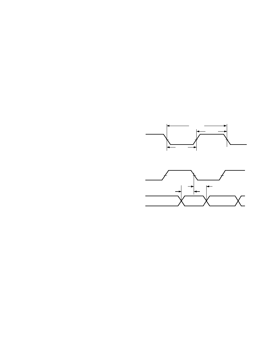
REV. 0
56
AD6635
Read/Write Chaining
The microport of the AD6635 allows for multiple accesses while
CSn is held low. The user can access multiple locations by
pulsing the
WR or RD line and changing the contents of the
external 3-bit address bus. External access to the external regis-
ters of Table XVI is accomplished in one of two modes using
the
CS0, CS1, RD, WR, and MODE inputs. The access modes
are Intel nonmultiplexed mode and Motorola nonmultiplexed
mode. These modes are controlled by the MODE input
(MODE = 0 for INM, MODE = 1 for MNM).
CS0, CS1, RD,
and
WR control the access type for each mode.
Intel Nonmultiplexed Mode (INM)
MODE must be tied low to operate the AD6635 microproces-
sor in INM mode. The access type is controlled by the user with
the
CS0, CS1, RD (DS), and WR (RW) inputs. The RDY
(
DTACK) signal is produced by the microport to communicate
to the user that an access has been completed. RDY (
DTACK)
goes low at the start of the access and is released when the inter-
nal access cycle is complete. See the timing diagrams for both
the read and write modes in the Specifications.
Motorola Nonmultiplexed Mode (MNM)
MODE must be tied high to operate the AD6635 microprocessor
in MNM mode. The access type is controlled by the user with
the
CS0, CS1, DS (RD), and RW (WR) inputs. The DTACK
(RDY) signal is produced by the microport to communicate to
the user that an access has been completed.
DTACK (RDY)
goes low when an internal access is complete and then will
return high after
DS (RD) is de-asserted. See the timing diagrams
for both the read and write modes in the Specifications.
SERIAL PORT CONTROL
The AD6635 has a two serial ports serving as a control inter-
face apart from the microport control interface. The serial port
input pin (SDI0) can access all of the internal registers for
Channels 03, control registers for Input/Output Ports A and
B, Half-band/AGCs A and B, and has preemptive access over
the microport. Similarly SDI4 can access all of the internal
registers for Channels 47, Input/Output Ports C and D, Half-
band/AGCs C and D, and has preemptive access over the
microport. In this manner, a single DSP could be used to
control the AD6635 over the serial port control interface.
The serial control port uses the serial clock (SCLK0 and SCLK4).
The serial input port is self-framing as described below, and
allows more efficient use of the serial input bandwidth for pro-
gramming. The beginning of a serial input frame is signaled by
a frame bit that appears on the SDI pin. This is the MSB of the
serial input frame. After the frame bit has been sampled high on
the falling edge of SCLK, a state counter will start and enable
an 11-bit serial shifter four serial clock cycles later. These four
SCLK cycles represent the "Don't Care" bits of the serial frame
that are ignored. After all of the bits are shifted, the serial input
port will pass along the 8-bit data and 3-bit address to the arbi-
tration block. This 8-bit data and 3-bit address set programs the
external memory explained in the Microport Control section.
Hence, serial port programming is similar to microport
programming.
The serial word structure for the SDI input is illustrated in
Figure 45. Only 15 bits are listed so that the second bit in a
standard 16-bit serial word is considered the frame bit. The
shifting order begins with frame and shifts the address, MSB
first, and then the data, MSB first.
Effectively, SDI0 and SCLK0 can program every register that
can otherwise be programmed using
CS0 on the microport.
Similarly SDI4 and SCLK4 can program every register that can
otherwise be programmed using
CS1 on the microport.
Serial Port Timing Specifications
The AD6635 serial control channel can operate only in the slave
mode (SCLK should be supplied by the programming device).
The diagrams below indicate the required timing for each of the
specification.
SCLKn
t
SCLK
t
SCLKH
t
SCLKL
Figure 43. SCLKn (n = 0, 4) Timing Requirements
t
SSI
SCLKn
SDIn
DATA
t
HSI
Figure 44. Serial Input Data Timing
Requirements, n = 0, 4
SDI0, SDI4
SDI is the serial data input. Serial data is sampled on the falling
edge of SCLK. This pin is used in the serial control mode to
write the internal control registers of the AD6635.
SCLK0, SCLK4
SCLK is a clock input, and the SDI input is sampled on the
falling edge of SCLK, and all outputs are switched on the rising
edge of SCLK. The maximum speed of this port is 65 MHz.
Bits 54 determine how the sample clock for the channel is
derived from the high speed CLK signal. There are four possible
choices. Each is defined below; for further detail the Numerically
Controlled Oscillator (NCO) section.
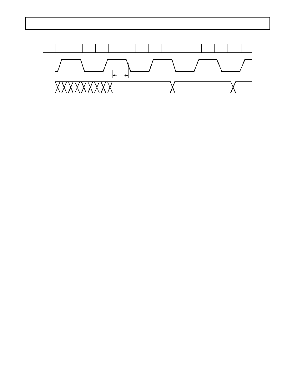
REV. 0
AD6635
57
t
SSI
CLKn
X DON'T CARE
FRAME
SCLK0
SCLK4
SDI0
SDI4
FRAME
X
X
X
X
A2
A1
A0
D7
D6
D5
D4
D3
D2
D1
D0
Figure 45. Serial Word Structure and Serial Port Control Timing

REV. 0
58
AD6635
INTERNAL WRITE ACCESS
Up to 20 bits of data (as needed) can be written by the process
described below. Any high order bytes that are needed are writ-
ten to the corresponding data registers defined in the external
3-bit address space. The least significant byte is then written to
DR0 at address (000). When a write to DR0 is detected, the
internal microprocessor port state machine then moves the data
in DR2DR0 to the internal address pointed to by the address
in the LAR and AMR.
Write Pseudocode
void write_micro(ext_address, int data);
main();
{
/* This code shows the programming of the NCO
phase offset register using the write_micro
function as defined above. The variable address
is the External Address A[2:0] and data is the
value to be placed in the external interface
register.
Internal Address = 0x87 */
// holding registers for NCO phase byte wide
access data
int d1, d0;
// NCO phase word (16-bits wide)
NCO_PHASE = 0xCBEF;
// write ACR
write_micro(7, 0x03 );
// write CAR
write_micro(6, 0x87);
// write DR1 with D[15:8]
d1 = (NCO_PHASE & 0xFF00) >> 8;
write_micro(1, d1);
// write DR0 with D[7:0]
// On this write all data is transferred to the
internal address
d0 = NCO_PHASE & 0xFF;
write_micro(0, d0);
} // end of main
INTERNAL READ ACCESS
A read is performed by first writing the CAR and AMR, as with
a write. The data registers (DR2DR0) are then read in the
reverse order that they were written. First, the least significant
byte of the data (D[7:0]) is read from DR0. On this transac-
tion, the high bytes of the data are moved from the internal
address pointed to by the CAR and AMR into the remaining
data registers (DR2DR1). This data can then be read from the
data registers using the appropriate 3-bit addresses. The num-
ber of data registers used depends solely on the amount of data
to be read or written. Any unused bit in a data register should
be masked out for a read.
Read Pseudocode
int read_micro(ext_address);
main();
{
/* This code shows the reading of the first
RCF coefficient using the read_micro function
as defined above. The variable address is the
External Address A[2..0].
Internal Address = 0x000
*/
// holding registers for the coefficient
int d2, d1, d0;
// coefficient (20-bits wide)
long coefficient;
// write AMR
write_micro(7, 0x00 );
// write LAR
write_micro(6, 0x00);
/* read D[7:0] from DR0, All data is moved
from the Internal Registers to the interface
registers on this access */
d0 = read_micro(0) & 0xFF;
// read D[15:8] from DR1
d1 = read_micro(1) & 0xFF;
// read D[23:16] from DR2
d2 = read_micro(2) & 0x0F;
coefficient = d0 + (d1 << 8) + (d2 << 16);
} // end of main
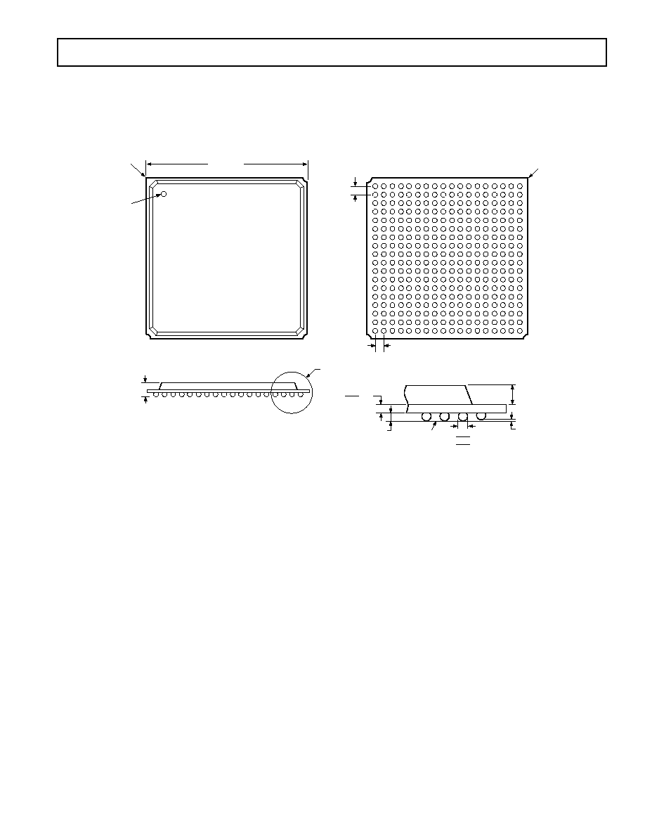
REV. 0
AD6635
59
OUTLINE DIMENSIONS
324-Lead Plastic Ball Grid Array [PBGA]
(B-324)
Dimensions shown in millimeters
TOP VIEW
2.50 MAX
SEATING
PLANE
0.20
DETAIL A
BALL DIAMETER
3.00 MAX
0.25 MIN
0.30 MIN
DETAIL A
3.50
MAX
19.00 SQ
1.00
BSC
1.00
BSC
BOTTOM VIEW
A
B
C
D
E
F
G
H
J
K
L
M
N
P
R
T
U
V
1
2
3
4
5
6
7
8
9
10
18 17 16 15 14 13 12 11
A1 BALL
CORNER
A1 BALL
CORNER
A1 BALL
INDICATOR
0.70
0.60
0.50
COMPLIANT TO JEDEC STANDARDS MS-034AAG-1

C0307302/03(0)
PRINTED IN U.S.A.
60
Document Outline
- FEATURES
- APPLICATIONS
- FUNCTIONAL BLOCK DIAGRAM
- GENERAL DESCRIPTION
- TABLE OF CONTENTS
- ARCHITECTURE
- SPECIFICATIONS
- RECOMMENDED OPERATING CONDITIONS
- ELECTRICAL CHARACTERISTICS
- GENERAL TIMING CHARACTERISTICS
- MICROPROCESSOR PORT TIMING CHARACTERISTICS
- ABSOLUTE MAXIMUM RATINGS
- ORDERING GUIDE
- PIN CONFIGURATION
- PIN CONFIGURATION (PIN OUT)
- PIN FUNCTION DESCRIPTION
- TIMING DIAGRAMS
- TIMING DIAGRAMS
INM Microport Mode (MODE = 0)
- TIMING DIAGRAMS
MNM Microport Mode (MODE = 1)
- INPUT DATA PORTS
- Input Data Format
- Input Timing
- Input Enable Control
- Gain Switching
- Input Data Scaling
- Scaling with Fixed-Point ADCs
- Scaling with Floating-Point or Gain-Ranging ADCs
- NUMERICALLY CONTROLLED OSCILLATOR
- Frequency Translation
- NCO Frequency Holdoff Register
- Phase Offset
- NCO Control Register
- Bypass
- Phase Dither
- Amplitude Dither
- Clear Phase Accumulator on Hop
- Input Enable Control
- Mode 00: Blank on IEN Low
- Mode 01: Clock on IEN High
- Mode 11: Clock on IEN Transition to Low
- WB Input Select
- Sync Select
- SECOND-ORDER rCIC FILTER
- rCIC2 Rejection
- Example Calculations
- Decimation and Interpolation Registers
- rCIC2 Scale
- FIFTH-ORDER CIC FILTER
- RAM COEFFICIENT FILTER
- RCF Decimation Register
- RCF Decimation Phase
- RCF Filter Length
- RCF Output Scale Factor and Control Register
- INTERPOLATING HALF-BAND FILTERS
- AUTOMATIC GAIN CONTROL
- The AGC Loop
- Desired Signal Level Mode
- Desired Clipping Level Mode
- Synchronization
- USER-CONFIGURABLE BUILT-IN SELF TEST (BIST)
- CHIP SYNCHRONIZATION
- Start
- Start with No Sync
- Start with Soft Sync
- Start with Pin Sync
- Hop
- Set Frequency No Hop
- Hop with Soft Sync
- Hop with Pin Sync
- PARALLEL OUTPUT PORTS
- Channel Mode
- AGC Mode
- Master/Slave PCLKn Modes
- Parallel Port Pin Functionality
- LINK PORT
- Link Port Data Format
- Link Port Timing
- TigerSHARC Configuration
- MEMORY MAP
- 0x00
0x7F: Coefficient Memory (CMEM)
- 0x80: Channel Sleep Register
- 0x81: Soft_SYNC Register
- 0x82: Pin_SYNC Register
- 0x83: Start Holdoff Counter
- 0X84: NCO FREQUENCY HOLDOFF COUNTER
- 0x85: NCO Frequency Register 0
- 0x86: NCO Frequency Register 1
- 0x87: NCO Phase Offset Register
- 0x88: NCO Control Register
- 0x90: rCIC2 Decimation
1 (MrCIC2
1)
- 0x91: rCIC2 Interpolation
1 (LrCIC2-1)
- 0x92: rCIC2 Scale
- 0x93:
- 0x94: CIC5 Decimation
1 (MCIC5
1)
- 0x95: CIC5 Scale
- 0x96:
- 0xA0: RCF Decimation
1 (MRCF
1)
- 0xA1: RCF Decimation Phase (PRCF)
- 0xA2: RCF Number of Taps Minus 1 (NRCF
1)
- 0xA3: RCF Coefficient Offset (CORCF)
- 0xA4: RCF Control Register
- 0xA5: BIST Register for I
- 0xA6: BIST Register for Q
- 0xA7: BIST Control Register
- 0xA8: RAM BIST Control Register
- 0xA9: Output Control Register
- Memory Map for Input Port Control Registers
- Input Port Control Registers
- 0x00 Lower Threshold A
- 0x01 Upper Threshold A
- 0x02 Dwell Time A
- 0x03 Gain Range A Control Register
- 0x04 Lower Threshold B
- 0x05 Upper Threshold B
- 0x06 Dwell Time B
- 0x07 Gain Range B Control Register
- Memory Map for Output Port Control Registers
- 0x08 Port A Control Register
- 0x09 Port B Control Register
- 0x0A AGC A Control Register
- 0x0B AGC A Holdoff Counter
- 0x0C AGC A Desired Level
- 0x0D AGC A Signal Gain
- 0x0E AGC A Loop Gain
- 0x0F AGC A Pole Location
- 0x10 AGC A Average Samples
- 0x11 AGC A Update Decimation
- 0x12 AGC B Control Register
- 0x13 AGC B Holdoff Counter
- 0x14 AGC B Desired Level
- 0x15 AGC B Signal Gain
- 0x16 AGC B Loop Gain
- 0x17 AGC B Pole Location
- 0x18 AGC B Average Samples
- 0x19 AGC B Update Decimation
- 0x1A Parallel Port Control A
- 0x1B Link Port Control A
- 0x1C Parallel Port Control B
- 0x1D Link Port Control B
- 0x1E Port Clock Control
- MICROPORT CONTROL
- External Memory Map
- Access Control Register (ACR)
- Channel Address Register (CAR)
- SOFT_SYNC Control Register
- PIN_SYNC Control Register
- SLEEP Control Register
- Data Address Registers
- Write Sequencing
- Read Sequencing
- Read/Write Chaining
- Intel Nonmultiplexed Mode (INM)
- Motorola Nonmultiplexed Mode (MNM)
- SERIAL PORT CONTROL
- Serial Port Timing Specifications
- SDI0, SDI4
- SCLK0, SCLK4
- INTERNAL WRITE ACCESS
- INTERNAL READ ACCESS
- OUTLINE DIMENSIONS