 | ÐлекÑÑоннÑй компоненÑ: AD6654CBC | СкаÑаÑÑ:  PDF PDF  ZIP ZIP |
AD6654 14-Bit, 92.16 MSPS, 4-/6-Channel Wideband IF to Baseband Receiver Data Sheet (Rev. 0)
14-Bit, 92.16 MSPS, 4-/6-Channel
Wideband IF to Baseband Receiver
AD6654
Rev. 0
Information furnished by Analog Devices is believed to be accurate and reliable.
However, no responsibility is assumed by Analog Devices for its use, nor for any
infringements of patents or other rights of third parties that may result from its use.
Specifications subject to change without notice. No license is granted by implication
or otherwise under any patent or patent rights of Analog Devices. Trademarks and
registered trademarks are the property of their respective owners.
One Technology Way, P.O. Box 9106, Norwood, MA 02062-9106, U.S.A.
Tel: 781.329.4700
www.analog.com
Fax: 781.461.3113
©2005 Analog Devices, Inc. All rights reserved.
FEATURES
SNR = 90 dB in 1.25 MHz bandwidth to Nyquist
SNR = 87 dB in 1.25 MHz bandwidth to 200 MHz
Integrated 14-bit, 92.16 MSPS ADC
IF sampling frequencies to 200 MHz
Internal 2.4 V reference, 2.2 V p-p analog input range
Internal differential track-and-hold analog input
Processes 4/6 wideband carriers simultaneously
Fractional clock multiplier to 200 MHz
Programmable decimating FIR filters, interpolating
half-band filters and programmable AGC loops
with 96 dB range
Three 16-bit configurable parallel output ports
User-configurable built-in self-test (BIST) capability
8-/16-bit microport and SPORT/SPI® serial port control
APPLICATIONS
Multicarrier, multimode digital receivers
GSM, EDGE, PHS, UMTS, WCDMA, CDMA2000,
TD-SCDMA, WiMAX
Micro and pico cell systems, software radios
Wireless local loop
Smart antenna systems
In-building wireless telephony
Broadband data applications
Instrumentation and test equipment
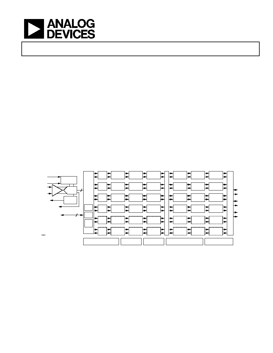
FUNCTIONAL BLOCK DIAGRAM
MRCF
DRCF
M = 116
CRCF
M = 116
LHB
L = 1, 2
MRCF
DRCF
M = 116
CRCF
M = 116
LHB
L = 1, 2
MRCF
DRCF
M = 116
CRCF
M = 116
LHB
L = 1, 2
MRCF
DRCF
M = 116
CRCF
M = 116
LHB
L = 1, 2
MRCF
DRCF
M = 116
CRCF
M = 116
LHB
L = 1, 2
MRCF
DRCF
M = 116
CRCF
M = 116
LHB
L = 1, 2
NCO
CIC5
M = 132
FIR1
HB1
M = BYP, 2
FIR2
HB2
M = BYP, 2
NCO
CIC5
M = 132
FIR1
HB1
M = BYP, 2
FIR2
HB2
M = BYP, 2
NCO
CIC5
M = 132
FIR1
HB1
M = BYP, 2
FIR2
HB2
M = BYP, 2
NCO
CIC5
M = 132
FIR1
HB1
M = BYP, 2
FIR2
HB2
M = BYP, 2
NCO
CIC5
M = 132
FIR1
HB1
M = BYP, 2
FIR2
HB2
M = BYP, 2
NCO
CIC5
M = 132
FIR1
HB1
M = BYP, 2
FIR2
HB2
M = BYP, 2
AGC
PA
PB
PC
DATA ROUTING
PARALLEL PORTS
DATA ROUTE
R
MATRIX
INPUT
MATRIX
AVDD, DRVDD,
VDDCORE, VDDIO, GND
SYNC
0, 1, 2, 3
8-BIT/16-BIT MICROPORT
INTERFACE
SPORT/
SPI INTERFACE
PEAK/
RMS
MSMT
EXP
BITS
PRN
GEN
SHA
AIN+
AIN
INTERNAL
TIMING
ENC+
ENC
ADC
V
REF
2.4V
V
REF
OVR
(ADC OVERRANGE)
EXP
(VGA LEVEL CONTROL)
M = DECIMATION
L = INTERPOLATION
05156-001
(AVAILABLE IN
6-CHANNEL MODEL ONLY)
4-CHANNEL AND 6-CHANNEL DIGITAL DOWN CONVERTER
CLOCK
MULTIPLIER
14-BIT ADC FRONT END
14
3
Figure 1.

AD6654
Rev. 0 | Page 2 of 88
TABLE OF CONTENTS
General Description ......................................................................... 4
Product Highlights ....................................................................... 5
Specifications..................................................................................... 6
Recommended Operating Conditions ...................................... 6
ADC DC Specifications ............................................................... 6
ADC Digital Specifications ......................................................... 6
ADC Switching Specifications.................................................... 7
ADC AC Specifications ............................................................... 7
Electrical Characteristics............................................................. 8
Timing Characteristics ................................................................ 9
Microport Timing Characteristics ........................................... 10
Serial Port Timing Characteristics ........................................... 11
Timing Diagrams............................................................................ 12
Absolute Maximum Ratings.......................................................... 18
Thermal Characteristics ............................................................ 18
Explanation of Test Levels ......................................................... 18
ESD Caution................................................................................ 18
Pin Configuration and Function Descriptions........................... 19
Typical Performance Characteristics ........................................... 22
ADC Equivalent Circuits............................................................... 25
Terminology .................................................................................... 26
Theory of Operation ...................................................................... 27
ADC Architecture ...................................................................... 27
Application information ................................................................ 28
ADC Configuration Notes ........................................................ 28
DDC Configuration Notes ........................................................ 29
ADC Input Port Monitor Function.............................................. 31
Peak Detector Mode................................................................... 31
Mean Power Mode ..................................................................... 31
Threshold Crossing Mode......................................................... 32
Additional Control Bits ............................................................. 32
Input Crossbar Matrix ............................................................... 33
Numerically Controlled Oscillator (NCO) ................................. 34
NCO Frequency.......................................................................... 34
Mixer............................................................................................ 35
Bypass .......................................................................................... 35
Clear Phase Accumulator on Hop ........................................... 35
Phase Dither................................................................................ 35
Amplitude Dither ....................................................................... 35
NCO Frequency Hold-Off Register ......................................... 35
Phase Offset................................................................................. 35
HOP Sync .................................................................................... 35
Fifth-Order CIC Filter ................................................................... 36
Bypass .......................................................................................... 36
CIC Rejection.............................................................................. 36
Example Calculations ................................................................ 37
FIR Half-Band Block...................................................................... 38
3-Tap Fixed coefficient Filter (FIR1) ....................................... 38
Decimate-by-2 Half-Band Filter (HB1) .................................. 38
6-Tap Fixed Coefficient Filter (FIR2) ...................................... 39
Decimate-by-2 Half-Band Filter (HB2) .................................. 39
Intermediate Data Router.............................................................. 41
Mono-Rate RAM Coefficient Filter (MRCF) ............................. 42
Symmetry .................................................................................... 42
Clock Rate ................................................................................... 42
Bypass .......................................................................................... 42
Scaling.......................................................................................... 42
Decimating RAM Coefficient Filter (DRCF) ............................. 43
Bypass .......................................................................................... 43
Scaling.......................................................................................... 43
Symmetry .................................................................................... 43
Coefficient Offset ....................................................................... 43

AD6654
Rev. 0 | Page 3 of 88
Decimation Phase .......................................................................43
Maximum Number of Taps Calculated....................................43
Programming DRCF Registers for
an Asymmetrical Filter ...............................................................44
Programming DRCF Registers for a Symmetric Filter ..........44
Channel RAM Coefficient Filter (CRCF) ....................................45
Bypass ...........................................................................................45
Scaling...........................................................................................45
Symmetry .....................................................................................45
Coefficient Offset ........................................................................45
Decimation Phase .......................................................................45
Maximum Number of TAPS Calculated..................................45
Programming CRCF Registers for an
Asymmetrical Filter ....................................................................46
Programming CRCF Registers for a Symmetrical Filter .......46
Interpolating Half-Band Filter.......................................................47
Output Data Router ........................................................................48
Interleaving Data.........................................................................48
Automatic Gain Control.................................................................49
AGC Loop ....................................................................................49
Desired Signal Level Mode ........................................................50
Desired Clipping Level Mode....................................................52
AGC Synchronization.................................................................52
SYNC Process ..............................................................................52
Parallel Port Output ........................................................................53
Interleaved I/Q Mode .................................................................53
Parallel IQ Mode .........................................................................53
Master/Slave PCLK Modes ........................................................55
Parallel Port Pin Functions ........................................................56
User-Configurable Built-In Self-Test (BIST) ...............................57
Chip Synchronization .....................................................................58
Start ...............................................................................................58
HOP ..............................................................................................58
Serial Port Control ..........................................................................60
Hardware Interface .....................................................................60
SPI Mode Timing........................................................................62
SPORT Mode Timing.................................................................64
Programming Indirect Addressed Registers
Using Serial Port..........................................................................67
Connecting the AD6654 Serial Port to a Blackfin DSP .........69
Microport .........................................................................................70
Intel (Inm) Mode ........................................................................70
Motorola (MNM) Mode ............................................................70
Accessing Multiple AD6654 Devices .......................................71
Memory Map ...................................................................................72
Reading the Memory Map Table...............................................72
Bit Format ....................................................................................72
Open Locations ...........................................................................72
Default Values..............................................................................72
Logic Levels..................................................................................72
Global Register Map ...................................................................74
Input Port Register Map.............................................................76
Channel Register Map ................................................................78
MRCF Coefficient Memory.......................................................79
Output Port Register Map..........................................................82
DDC Design Notes .........................................................................85
Outline Dimensions........................................................................87
Ordering Guide ...........................................................................87
REVISION HISTORY
4/05--Revision 0: Initial Version

AD6654
Rev. 0 | Page 4 of 88
GENERAL DESCRIPTION
The AD6654 is a mixed-signal IF-to-baseband receiver
consisting of a 14-bit, 92.16 MSPS analog-to-digital converter
(ADC) and a 4-/6-channel, multimode digital down-converter
(DDC) capable of processing up to six WCDMA (wideband
code division multiple access) channels. The AD6654 has been
optimized for the demanding filtering requirements of wide-
band standards such as CDMA2000, UMTS, and TD-SCDMA,
but is flexible enough to support wider standards such as
WiMAX. It is typically used as part of a radio system that
digitally demodulates and filters IF sampled signals.
The ADC stage features a high performance track-and-hold
input amplifier (T/H), integrated voltage reference, and 14-bit
sampling resolution. Input signals up to 200 MHz can be
accurately digitized at encode rates up to 92.16 MSPS. The ADC
data outputs are internally routed directly into the DDC inputs,
where down-conversion, decimation and digital filtering are
performed. An overrange (OVR) output bit provides indication
of excessive ADC input levels. An ADC data-ready (DR) output
bit provides a synchronized clock for the integrated DDC.
Data from the ADC is evaluated for peak or mean power in the
input stage of the DDC, and the result is available to the user via
control register access. The DDC input stage also outputs 3-bit
level-indicator data (EXP) bits that can be used to control the
gain of the external DVGA in 6 dB steps (up to 48 dB) to
optimize signal amplitude into the ADC input.
The DDC stage has the following signal processing stages: six
WCDMA-ready channels, each consisting of a frequency
translator, a fifth-order cascaded integrated comb filter, two sets
of cascaded fixed coefficient FIR and half-band filters, three
cascaded programmable sum of product FIR filters, an
interpolating half-band filter (IHB), and a digital automatic
gain control (AGC) block. Multiple modes are supported for
clocking data out of the chip. Programming is accomplished via
serial or microport interfaces.
Frequency translation is accomplished with a 32-bit complex
numerically controlled oscillator (NCO). The NCO has greater
than 110 dBc SDFR. This stage translates a real input signal
from an intermediate frequency (IF) to a baseband complex
digital output. Phase and amplitude dither can be enabled on-
chip to improve spurious performance of the NCO. A 16-bit
phase-offset word is available to create a known phase relation-
ship between multiple AD6654 chips or channels. The NCO can
also be bypassed.
Following frequency translation is a fifth-order CIC filter with a
programmable decimation between 1 and 32. This filter is used
to efficiently lower the sample rate, while providing sufficient
alias rejection at frequencies at higher offsets from the signal
of interest.
Following the CIC5 are two sets of filters. Each filter set
includes a nondecimating FIR filter and a decimate-by-2 half-
band filter. The FIR1 filter provides about 30 dB of rejection,
while the HB1 provides about 77 dB of rejection. These two sets
of filters can be used together to achieve a 107 dB stop-band
alias rejection, or they can be individually bypassed to save
power.
The FIR2 filter provides about 30 dB of rejection, while the HB2
filter provides about 65 dB of rejection. The filters can be used
together to achieve more than 95 dB stop-band alias rejection,
or they can be individually bypassed to save power. FIR1 and
HB1 filters can run at the maximum ADC data port rate. In
contrast, FIR2 and HB2 can run with a maximum input rate of
75 MSPS (input rate to FIR2 and HB2 filters).
The programmable filtering is divided into three cascaded RAM
coefficient filters (RCFs) for flexible and power-efficient
filtering. The first filter in the cascade is the MRCF, consisting
of a programmable nondecimating FIR. It is followed by
programmable FIR filters (DRCF) with decimation from 1 to
16. They can be used either together to provide high rejection
filters, or independently to save power. The maximum input
rate to the MRCF is one-fourth the PLL clock rate.
The CRCF (Channel RCF) is the last programmable FIR filter
with programmable decimation from 1 to 16. It is typically used
to meet the spectral mask requirements for the air standard of
interest. This could be an RRC, antialiasing filter or any other
real data filter. Decimation in preceding blocks is used to keep
the input rate of this stage as low as possible for the best filter
performance.
The last filter stage in the chain is an interpolate-by-2 half-band
filter, which is used to up-sample the CRCF output to produce
higher output oversampling. Signal rejection requirements for
this stage are relaxed, because preceding filters have already
filtered the blockers and adjacent carriers.
The DDC input port of the AD6654 has its own clock input
used for latching the input data, as well as for providing the
input for an onboard PLL clock multiplier. The output of the
PLL clock is used for processing all filters and processing blocks
beyond the data router following CIC filter. The PLL clock can
be programmed to have a maximum clock rate of 200 MHz.
Typically, the DDC input clock is driven directly from the
integrated ADC's data-ready (DR) output to ensure proper
synchronization.
A data routing block is used to distribute data from the CICs to
the various channel filters. This block allows multiple back-end
filter chains to work together to process high bandwidth signals
or to make even sharper filter transitions than a single channel

AD6654
Rev. 0 | Page 5 of 88
can perform. It can also allow complex filtering operations to be
achieved in the programmable filters.
The digital AGC provides the user with scaled digital outputs
based on the rms level of the signal present at the output of the
digital filters. The user can set the requested level and time
constant of the AGC loop for optimum performance of the
postprocessor. This is a critical function in the base station for
CDMA application, where the power level must be well
controlled going into the RAKE receivers. It has programmable
clipping and rounding control to provide different output
resolutions.
The overall filter response for the AD6654 is the composite of
all the combined filter stages. Each successive filter stage is
capable of narrower transition bandwidths, but requires a
greater number of CLK cycles to calculate the output. The
AD6654 features a fractional clock multiplier that uses the ADC
clock (which is slower than the DDC's processing speed) to
produce a DDC master clock up to 200 MHz. This feature
allows fractional multiplication of the input clock to allow the
DDC to function at maximum speed while maintaining edge
identity to the ADC clock.
More decimation in the first filter stage minimizes overall
power consumption. Data from the device is interfaced to a
DSP/FPGA/baseband processor via high speed parallel ports
(preferred), or a DSP-compatible microprocessor interface.
The AD6654 is available in 4-channel and 6-channel versions.
The primary focus of the data sheet is on the 6-channel part.
The only difference between the 6-channel and 4-channel
devices is that, on the 4-channel version, Channel 4 and
Channel 5 are not available (see Figure 1). The 4-channel device
has the same DDC input port features, output ports, and
memory map as the 6-channel device. On the 4-channel
version, the memory map section for Channel 4 and Channel 5
can be programmed and read back, but the two extra channels
are disabled internally.
PRODUCT HIGHLIGHTS
1.
Integrated 14-bit, 92.16 MSPS ADC.
2.
Track-and-hold amplifier analog input for excellent IF
sampling up to 200 MHz.
3.
Four or six independent digital filtering channels.
4.
RMS/peak power monitoring of the ADC data port and
96 dB range AGCs before the output ports.
5.
Three programmable RAM coefficient filters, three half-
band filters, two fixed coefficient filters, and one fifth-
order CIC filter per channel.
6.
Complex filtering by combining filtering capability of
multiple channels.
7.
Three 16-bit parallel output ports operating at up to
200 MHz clock.
8.
Blackfin®- and TigerSHARC®-compatible, 8-/16-bit
microprocessor port.
9.
Synchronous serial communications port is compatible
with most serial interface standards: SPORT, SPI, and SSR.

AD6654
Rev. 0 | Page 6 of 88
SPECIFICATIONS
RECOMMENDED OPERATING CONDITIONS
Table 1.
Parameter (Conditions)
Temp
Test Level
Min
Typ
Max
Unit
AVDD
1
Full IV
4.75
5.0
5.25
V
DRVDD
2
Full IV
3.0
3.3
3.6
V
VDDCORE Full
IV
1.65
1.8
1.95
V
VDDIO
2
Full IV
3.0
3.3
3.6
V
T
AMBIENT
IV
-25
+25
+85
°C
1
Specified for dc supplies with linear rise-time <250 ms.
2
DRVDD and VDDIO can be operated from the same supply.
ADC DC SPECIFICATIONS
AVDD = 5.0 V, DRVDD = 3.3 V, VDDCORE = 1.8 V, VDDIO = 3.3 V, maximum rated sample rate, differential ENC and AIN, unless
otherwise noted.
Table 2.
Parameter (Conditions)
Temp
Test Level
Min
Typ
Max
Unit
RESOLUTION
Full
IV
14
Bits
INTERNAL VOLTAGE REFERENCE (V
REF
)
1
Output Voltage
Full
IV
2.4
V
ANALOG INPUTS
Differential Input Voltage Range
Full
IV
2.2
V p-p
Differential Input Capacitance
Full
V
1.5
pF
Differential Input Resistance
Full
V
1
k
Power Supply Rejection (PSRR)
25°C
V
±1.0
mV/V
1
V
REF
is provided for setting the common-mode offset of a differential amplifier such as the AD8138 when a dc-coupled analog input is required. V
REF
should be buffered
if used to drive additional circuit functions.
ADC DIGITAL SPECIFICATIONS
AVDD = 5.0 V, DRVDD = 3.3 V, VDDCORE = 1.8 V, VDDIO = 3.3 V, maximum rated sample rate, differential ADC input, unless
otherwise noted.
Table 3.
Parameter (Conditions)
Temp
Test Level
Min
Typ
Max
Unit
ENCODE INPUTS (ENC+, ENC-)
Differential Input Voltage
Full
IV
0.4
V p-p
Differential Input Resistance
25°C
V
10
k
Differential Input Capacitance
25°C
V
2.5
pF

AD6654
Rev. 0 | Page 7 of 88
ADC SWITCHING SPECIFICATIONS
AVDD = 5.0 V, DRVDD = 3.3 V, VDDCORE = 1.8 V, VDDIO = 3.3 V, maximum rated sample rate, differential input, unless
otherwise noted.
Table 4.
Parameter (Conditions)
Temp
Test Level
Min
Typ
Max
Unit
SWITCHING PERFORMANCE
Maximum Conversion Rate
Full
II
92.16
MSPS
Minimum Conversion Rate
Full
IV
30
MSPS
ENC Pulse Width High
1
(t
ENCH
)
Full
IV
5.154
5.425
ns
ENC Pulse Width Low
1
(t
ENCL
)
Full
IV
5.154
5.425
ns
1
Several internal timing parameters are a function of t
ENCL
and t
ENCH
, optimum performance will be achieved with 50/50 duty cycle.
ADC AC SPECIFICATIONS
AVDD = 5.0 V, DRVDD = 3.3 V, VDDCORE = 1.8 V, VDDIO = 3.3 V, maximum rated sample rate, differential input, unless
otherwise noted.
Table 5.
Parameter (Conditions)
Temp
Test Level
Min
Typ
Max
Unit
SIGNAL-TO-NOISE RATIO
1
(WITHOUT HARMONICS)
Analog Input Frequency 37 MHz
ADC (46.08 MHz BW)
25°C
V
74.5
dB
CDMA (1.25 MHz BW)
Full
II
88
90.0
dB
WCDMA (5.0 MHz BW)
25°C
V
84
dB
Analog Input Frequency 70 MHz
ADC (46.08 MHz BW)
25°C
V
73.5
dB
CDMA (1.25 MHz BW)
Full
II
87.5
89
dB
WCDMA (5.0 MHz BW)
25°C
V
83
dB
Analog Input Frequency 150 MHz
ADC (46.08 MHz BW)
25°C
V
73
dB
CDMA (1.25 MHz BW)
25°C
V
88
dB
WCDMA (5.0 MHz BW)
25°C
V
82
dB
Analog Input Frequency 200 MHz
ADC (46.08 MHz BW)
25°C
V
72
dB
CDMA (1.25 MHz BW)
25°C
V
87
dB
WCDMA (5.0 MHz BW)
25°C
V
81
dB
WORST HARMONIC
2
(ANALOG INPUT @ -1 dBFS)
37 MHz
Full
II
85
93
dBc
70 MHz
Full
V
91
dBc
150 MHz
Full
V
71
dBc
200 MHz
Full
V
63
dBc
INTERMODULATION DISTORTION (TWO-TONES SEPARATED BY 1 MHz)
3
Analog Input = 55/56 MHz
25°C
V
90
dBc
ANALOG INPUT BANDWIDTH
25°C
V
270
MHz
1
Analog input =
-1 dB below full scale.
2
Includes Harmonic 2 through Harmonic 6.
3
Analog input = each
-7 dB below full scale.

AD6654
Rev. 0 | Page 8 of 88
ELECTRICAL CHARACTERISTICS
AVDD = 5.0 V, DRVDD = 3.3 V, VDDCORE = 1.8 V, VDDIO = 3.3 V, maximum rated sample rate, differential input, unless
otherwise noted.
Table 6.
Parameter (Conditions)
Temp
Test Level
Min
Typ
Max
Unit
LOGIC INPUTS (NOT 5 V TOLERANT)
Logic Compatibility
Full
IV
3.3 V CMOS
Logic 1 Voltage
Full
IV
2.0
3.6
V
Logic 0 Voltage
Full
IV
-0.3
+0.8
V
Logic 1 Current
Full
IV
1
10
µA
Logic 0 Current
Full
IV
1
10
µA
Logic 1 Current (Inputs With Pull-Down)
Full
IV
Logic 0 Current (Inputs With Pull-Up)
Full
IV
Input Capacitance
25°C
V
4
pF
LOGIC OUTPUTS
Logic Compatibility
Full
IV
3.3 V CMOS
Logic 1 Voltage (I
OH
= 0.25 mA)
Full
IV
2.4
VDDIO - 0.2
V
Logic 0 Voltage (I
OL
= 0.25 mA)
Full
IV
0.2
0.4
V
SUPPLY CURRENTS
WCDMA (92.16 MSPS) EXAMPLE
1
I
AVDD
25°C
V
275
mA
I
DRVDD
25°C
V
32
mA
I
VDD
25°C
V
460
mA
I
VDDIO
25°C
V
60
mA
CDMA2000 (92.16 MSPS) EXAMPLE
1
I
AVDD
25°C
V
275
mA
I
DRVDD
25°C
V
32
mA
I
VDD
25°C
V
435
mA
I
VDDIO
25°C
V
25
mA
TDS-CDMA (76.8 MSPS) EXAMPLE
1
, 2
I
AVDD
25°C
V
275
mA
I
DRVDD
25°C
V
32
mA
I
VDD
25°C
V
250
mA
I
VDDIO
25°C
V
15
mA
TOTAL POWER DISSIPATION
WCDMA (92.16 MSPS)
1
25°C
V
2.5
W
CDMA2000 (92.16 MSPS)
1
25°C
V
2.3
W
TDS-CDMA (76.8 MSPS)
1, 2
25°C
V
2.0
W
1
ADC input port, all six DDC channels, and the relevant signal processing blocks are active.
2
PLL is turned off for power savings.

AD6654
Rev. 0 | Page 9 of 88
TIMING CHARACTERISTICS
Table 7.
Parameter
1, 2, 3
Temp
Test
Level
Min
Typ
Max
Unit
CLK TIMING REQUIREMENTS
t
CLK
CLK Period
Full
IV
10.85
ns
t
CLKL
CLK Width Low
Full
IV
5.154
0.5 × t
CLK
ns
t
CLKH
CLK Width High
Full
IV
5.154
0.5 × t
CLK
ns
INPUT WIDEBAND DATA TIMING REQUIREMENTS
t
DEXP
CLK to EXP[2:0] Delay
Full IV
5.98
10.74
ns
PARALLEL OUTPUT PORT TIMING REQUIREMENTS (MASTER)
t
DPREQ
PCLK to Px REQ Delay (x = A, B, C)
Full IV
1.77
3.86 ns
t
DPP
PCLK to Px[15:0] Delay (x = A, B, C)
Full IV
2.07
5.29 ns
t
DPIQ
PCLK to Px IQ Delay (x = A, B, C)
Full IV
0.48
5.49 ns
t
DPCH
PCLK to Px CH[2:0] Delay (x = A, B, C)
Full IV
0.38
5.35 ns
t
DPGAIN
PCLK to Px Gain Delay (x = A, B, C)
Full IV
0.23
4.95 ns
t
SPA
Px ACK to
PCLK Setup Time (x = A, B, C)
Full IV
4.59
ns
t
HPA
Px ACK to
PCLK Hold Time (x = A, B, C)
Full IV
0.90
ns
PARALLEL OUTPUT PORT TIMING REQUIREMENTS (SLAVE)
t
PCLK
PCLK Period
Full
IV
5.0
ns
t
PCLKL
PCLK Low Period
Full
IV
1.7
0.5 × t
PCLK
ns
t
PCLKH
PCLK High Period
Full
IV
0.7
0.5 × t
PCLK
ns
t
DPREQ
PCLK to Px REQ Delay (x = A, B, C)
Full IV
4.72
8.87 ns
t
DPP
PCLK to Px[15:0] Delay (x = A, B, C)
Full IV
4.8
8.48
ns
t
DPIQ
PCLK to Px IQ Delay (x = A, B, C)
Full IV
4.83
10.94
ns
t
DPCH
PCLK to Px CH[2:0] Delay (x = A, B, C)
Full IV
4.88
10.09
ns
t
DPGAIN
PCLK to Px Gain Delay (x = A, B, C)
Full IV
5.08
11.49
ns
t
SPA
Px ACK to
PCLK Setup Time (x = A, B, C)
Full IV
6.09
ns
t
HPA
Px ACK to
PCLK Hold Time (x = A, B, C)
Full IV
1.0
ns
MISC PINS TIMING REQUIREMENTS
t
RESET
RESET Width Low
Full IV
30
ns
t
DIRP
CPUCLK/SCLK to IRP Delay
Full V
7.5
ns
t
SSYNC
SYNC(0, 1, 2, 3) to
CLK Setup Time
Full IV
0.87
ns
t
HSYNC
SYNC(0, 1, 2, 3) to
CLK Hold Time
Full IV
0.67
ns
1
All timing specifications are valid over the VDDCORE range of 1.7 V to 1.9 V, and the VDDIO range of 3.0 V to 3.6 V.
2
C
LOAD
= 40 pF on all outputs, unless otherwise noted.
3
These timing parameters are derived from the ADC ENC rate with DDC CLK driven directly from ADC DR output.
AD6654
Rev. 0 | Page 10 of 88
MICROPORT TIMING CHARACTERISTICS
Table 8.
Parameter
1, 2
Temp
Test
Level
Min
Typ
Max
Unit
MICROPORT CLOCK TIMING REQUIREMENTS
t
CPUCLK
CPUCLK Period
Full
IV
10.0
ns
t
CPUCLKL
CPUCLK Low Time
Full
IV
1.53
0.5 × t
CPUCLK
ns
t
CPUCLKH
CPUCLK High Time
Full
IV
1.70
0.5 × t
CPUCLK
ns
INM MODE WRITE TIMING (MODE = 0)
t
SC
Control
3
to
CPUCLK Setup Time
Full IV
0.80
ns
t
HC
Control
3
to
CPUCLK Hold Time
Full IV
0.09
ns
t
SAM
Address/Data to
CPUCLK Setup Time
Full IV
0.76
ns
t
HAM
Address/Data to
CPUCLK Hold Time
Full IV
0.20
ns
t
DRDY
CPUCLK to RDY (DTACK) Delay
Full
IV
3.51
6.72 ns
t
ACC
Write Access Time
Full
IV
3 × t
CPUCLK
9 × t
CPUCLK
ns
INM MODE READ TIMING (MODE = 0)
t
SC
Control
3
to
CPUCLK Setup Time
Full
IV 1.00
ns
t
HC
Control
3
to
CPUCLK Hold Time
Full
IV 0.03
ns
t
SAM
Address to
CPUCLK Setup Time
Full
IV 0.80
ns
t
HAM
Address to
CPUCLK Hold Time
Full
IV 0.20
ns
t
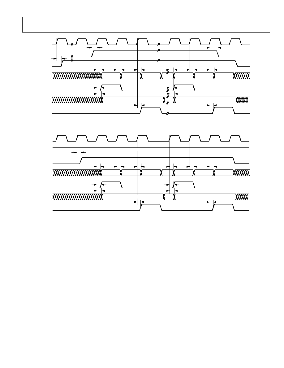
DD
CPUCLK to Data Delay
Full
V 5.0 ns
t
DRDY
CPUCLK to RDY (DTACK) Delay
Full
IV
4.50
6.72 ns
t
ACC
Read Access Time
Full
IV
3 × t
CPUCLK
9 × t
CPUCLK
ns
MNM MODE WRITE TIMING (MODE = 1)
t
SC
Control
3
to
CPUCLK Setup Time
Full IV
1.00
ns
t
HC
Control
3
to
CPUCLK Hold Time
Full IV
0.00
ns
t
SAM
Address/Data to
CPUCLK Setup Time
Full
IV
0.00
ns
t
HAM
Address/Data to
CPUCLK Hold Time
Full
IV
0.57
ns
t
DDTACK
CPUCLK to DTACK (RDY) Delay
Full
IV
4.10
5.72 ns
t
ACC
Write Access Time
Full
IV
3 × t
CPUCLK
9 × t
CPUCLK
ns
MNM MODE READ TIMING (MODE = 1)
t
SC
Control
3
to
CPUCLK Setup Time
Full IV
1.00
ns
t
HC
Control
3
to
CPUCLK Hold Time
Full IV
0.00
ns
t
SAM
Address to
CPUCLK Setup Time
Full IV
0.00
ns
t
HAM
Address to
CPUCLK Hold Time
Full IV
0.57
ns
t
DD
CPUCLK to Data Delay
Full
V
5.0
ns
t
DDTACK
CPUCLK to DTACK (RDY) Delay
Full
IV
4.20
6.03 ns
t
ACC
Read Access Time
Full
IV
3 × t
CPUCLK
9 × t
CPUCLK
ns
1
All timing specifications are valid over the VDDCORE range of 1.7 V to 1.9 V, and the VDDIO range of 3.0 V to 3.6 V.
2
C
LOAD
= 40 pF on all outputs, unless otherwise noted.
3
Specification pertains to control signals: R/W, (WR), DS, (RD), and CS.
AD6654
Rev. 0 | Page 11 of 88
SERIAL PORT TIMING CHARACTERISTICS
Table 9.
Parameter
1, 2, 3
Temp
Test Level
Min
Typ
Max
Unit
SERIAL PORT CLOCK TIMING REQUIREMENTS
t
SCLK
SCLK Period
Full
IV
10.0
ns
t
SCLKL
SCLK Low Time
Full
IV
1.60
0.5 × t
SCLK
ns
t
SCLKH
SCLK High Time
Full
IV
1.60
0.5 × t
SCLK
ns
SPI PORT CONTROL TIMING REQUIREMENTS (MODE = 0)
t
SSDI
SDI to
SCLK Setup Time
Full IV
1.30
ns
t
HSDI
SDI to
SCLK Hold Time
Full IV
0.40
ns
t
SSCS
SCS to
SCLK Setup Time
Full IV
4.12
ns
t
HSCS
SCS to
SCLK Hold Time
Full IV
-2.78
ns
t
DSDO
SCLK to SDO Delay Time
Full
IV
4.28
7.96
ns
SPORT MODE CONTROL TIMING REQUIREMENTS (MODE = 1)
t
SSDI
SDI to
SCLK Setup Time
Full IV
0.80
ns
t
HSDI
SDI to
SCLK Hold Time
Full IV
0.40
ns
t
SSRFS
SRFS to
SCLK Setup Time
Full IV
1.60
ns
t
HSRFS
SRFS to
SCLK Hold Time
Full IV
-0.13
ns
t
SSTFS
STFS to
SCLK Setup Time
Full IV
1.60
ns
t
HSTFS
STFS to
SCLK Hold Time
Full IV
-0.30
ns
t
SSCS
SCS to
SCLK Setup Time
Full IV
4.12
ns
t
HSCS
SCS to
SCLK Hold Time
Full IV
-2.76
ns
t
DSDO
SCLK to SDO Delay Time
Full IV
4.29
7.95
ns
1
All timing specifications are valid over the VDDCORE range of 1.7 V to 1.9 V and the VDDIO range of 3.0 V and 3.6 V.
2
C
LOAD
= 40 pF on all outputs, unless otherwise noted.
3
SCLK rise/fall time should be 3 ns maximum.
AD6654
Rev. 0 | Page 12 of 88
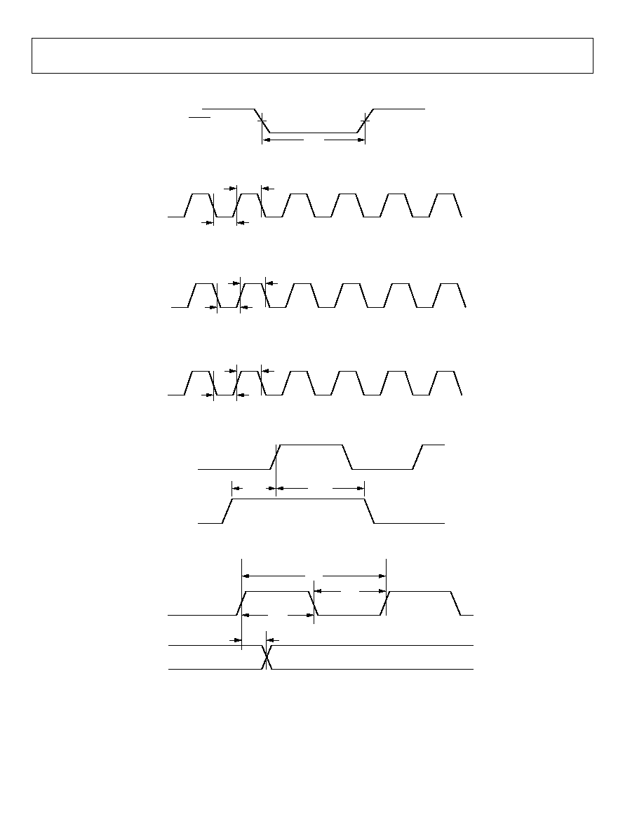
TIMING DIAGRAMS
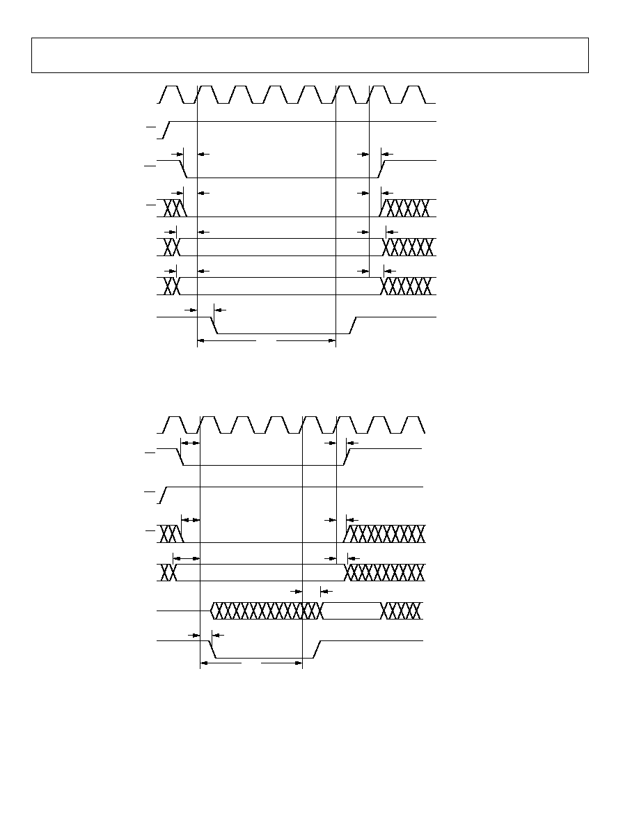
05156-002
RESET
t
RESL
Figure 2. Reset Timing Requirements
CLK
t
CLKH
t
CLKL
05156-003
Figure 3. CLK Switching Characteristics
CPUCLK
t
CPUCLKL
t
CPUCLKH
05156-004
Figure 4. CPUCLK Switching Characteristics
SCLK
t
SCLKH
t
SCLKL
05156-005
Figure 5. SCLK Switching Characteristics
SYNC [3:0]
CLK
t
HSYNC
t
SSYNC
05156-006
Figure 6. SYNC Timing Inputs
EXPx [2:0]
CLK
t
DEXP
t
CLK
t
CLKL
t
CLKH
05156-007
Figure 7. Gain Control Word Output Switching Characteristics
AD6654
Rev. 0 | Page 13 of 88
05156-008
PCLK
t
DPREQ
PxREQ
PxACK
Px [15:0]
PxIQ
PxCH [2:0]
PxGAIN
I [15:0]
Q [15:0]
I [15:0]
Q [15:0]
RSSI [11:0]
RSSI [11:0]
PxCH [2:0] = CHANNEL NO.
PxCH [2:0] = CHANNEL NO.
t
DPGAIN
t
DPP
t
DPP
t
DPP
t
DPIQ
t
DPCH
t
DPP
t
DPIQ
t
DPCH
t
DPGAIN
t
SPA
t
DPP
t
DPP
t
HPA
Figure 8. Master Mode PxACK to PCLK Switching Characteristics
PCLK
t
DPREQ
PxREQ
PxACK
Px [15:0]
PxIQ
PxCH [2:0]
PxGAIN
TIED LOGIC HIGH ALL THE TIME
I [15:0]
Q [15:0]
I [15:0]
Q [15:0]
RSSI [11:0]
RSSI [11:0]
PxCH [2:0] = CHANNEL NO.
PxCH [2:0] = CHANNEL NO.
t
DPGAIN
t
DPP
t
DPP
t
DPP
t
DPIQ
t
DPCH
t
DPP
t
DPIQ
t
DPCH
t
DPGAIN
t
DPP
t
DPP
05156-009
Figure 9. Master Mode PxREQ to PCLK Switching Characteristics
AD6654
Rev. 0 | Page 14 of 88
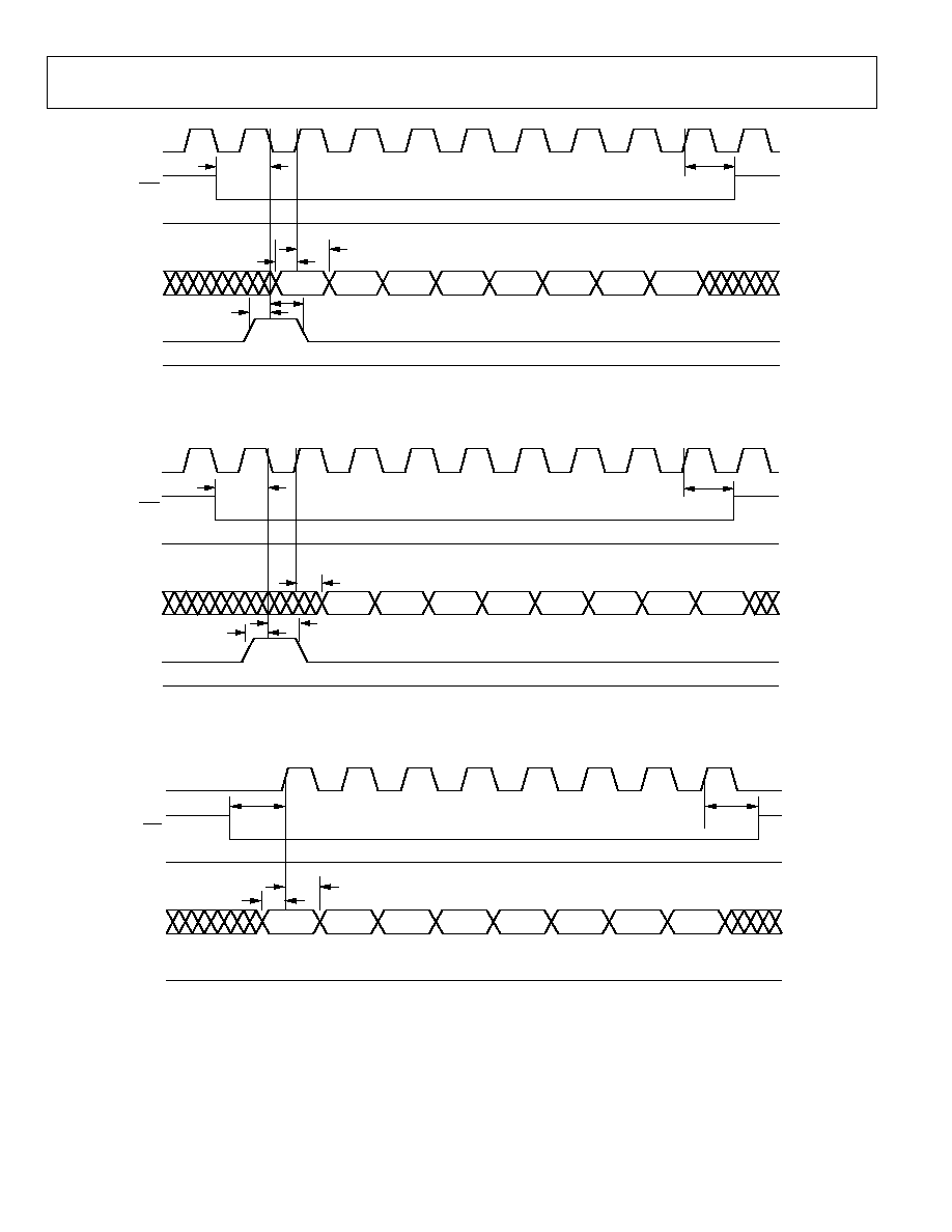
t
SAM
RD
WR
CS
A [7:0]
D [15:0]
RDY
VALID ADDRESS
VALID DATA
t
HAM
CPUCLK
NOTE:
t
ACC
ACCESS TIME DEPENDS ON THE ADDRESS ACCESSED. IT CAN VARY FROM 3 TO 9 CPUCLK CYCLES.
t
SC
t
SC
t
SAM
t
DRDY
t
HAM
t
HC
t
HC
t
ACC
05156-010
Figure 10. INM Microport Write Timing Requirements
RD
WR
CS
A [7:0]
D [15:0]
RDY
VALID ADDRESS
VALID DATA
CPUCLK
t
SC
t
SC
t
SAM
t
DD
t
DRDY
t
HC
t
HC
t
HAM
NOTE:
t
ACC
ACCESS TIME DEPENDS ON THE ADDRESS ACCESSED. IT CAN VARY FROM 3 TO 9 CPUCLK CYCLES.
t
ACC
05156-011
Figure 11. INM Microport Read Timing Requirements

AD6654
Rev. 0 | Page 15 of 88
t
SAM
DS
R/W
CS
A [7:0]
D [15:0]
DTACK
VALID ADDRESS
VALID DATA
t
SAM
t
HAM
t
DDTACK
NOTE:
t
ACC
ACCESS TIME DEPENDS ON THE ADDRESS ACCESSED. IT CAN VARY FROM 3 TO 9 CPUCLK CYCLES.
t
SC
t
HC
CPUCLK
t
HC
t
HC
t
HAM
t
SC
t
SC
05156-012
t
ACC
Figure 12. MNM Microport Write Timing Requirements
05156-013
t
SAM
DS
R/W
CS
A [7:0]
D [15:0]
VALID ADDRESS
VALID
DATA
t
HAM
t
DDTACK
NOTE:
t
ACC
ACCESS TIME DEPENDS ON THE ADDRESS ACCESSED. IT CAN VARY FROM 3 TO 9 CPUCLK CYCLES.
t
HC
CPUCLK
t
HC
t
HC
t
DD
t
SC
DTACK
t
SC
t
SC
t
ACC
Figure 13. MNM Microport Read Timing Requirements
AD6654
Rev. 0 | Page 16 of 88
SCS
SMODE
SDI
MODE
t
HSDI
t
SSDI
t
HSCS
LOGIC 1
LOGIC 1
SCLK
t
HSRFS
t
SSRFS
D0
D1
D2
D3
D4
D5
D6
D7
SRFS
t
SSCS
05156-014
Figure 14. SPORT Mode Write Timing Characteristics
SCS
SMODE
SDO
MODE
t
SSCS
t
DSDO
t
HSCS
LOGIC 1
LOGIC 1
SCLK
t
HSTFS
t
SSTFS
STFS
D0
D1
D2
D3
D4
D5
D6
D7
05156-015
Figure 15. SPORT Mode Read Timing Characteristics
05156-016
SCS
SMODE
SDI
MODE
t
SSCS
t
HSDI
D0
D1
D2
D3
D4
D5
D6
D7
t
SSDI
t
HSCS
LOGIC 1
LOGIC 0
SCLK
Figure 16. SPI Mode Write Timing Characteristics
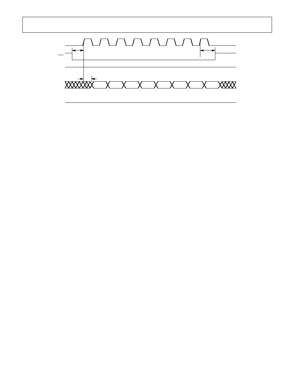
AD6654
Rev. 0 | Page 17 of 88
SCLK
SCS
SMODE
SDO
MODE
t
SSCS
t
DSDO
D0
D1
D2
D3
D4
D5
D6
D7
t
HSCS
LOGIC 0
LOGIC 0
05156-017
Figure 17. SPI Mode Read Timing Characteristics

AD6654
Rev. 0 | Page 18 of 88
ABSOLUTE MAXIMUM RATINGS
Table 10.
Parameter Rating
AVDD
0 to +7.0 V
DRVDD
0 to +4.0 V
VDDCORE
-0.3 V to +2.2 V
VDDIO
0 to +4.0 V
Analog/Encode Input Voltage
0 to AVDD
Analog Input Current
25 mA
Digital Input Voltage
-0.3 V to + 3.6 V (not 5 V
tolerant)
Digital Output Voltage
-0.3 V to VDDIO + 0.3 V
Operating Temperature Range
(Ambient)
-25°C to +85°C
Junction Temperature Under Bias
150°C
Storage Temperature Range
-65°C to +150°C
Stresses above those listed under Absolute Maximum Ratings
may cause permanent damage to the device. This is a stress
rating only; functional operation of the device at these or any
other conditions above those indicated in the operational
section of this specification is not implied. Exposure to absolute
maximum rating conditions for extended periods may affect
device reliability.
THERMAL CHARACTERISTICS
256 BGA, 17 mm sq.
JA
= 21°C/W, no airflow.
Estimate based on JEDEC JC51-2 model using horizontally
positioned 4-layer board.
EXPLANATION OF TEST LEVELS
Test Level
Description
I
100% production tested.
II
100% production tested at 25°C.
III
Sample tested only.
IV
Parameter guaranteed by design and analysis.
V
Parameter is typical value only.
ESD CAUTION
ESD (electrostatic discharge) sensitive device. Electrostatic charges as high as 4000 V readily accumulate on
the human body and test equipment and can discharge without detection. Although this product features
proprietary ESD protection circuitry, permanent damage may occur on devices subjected to high energy
electrostatic discharges. Therefore, proper ESD precautions are recommended to avoid performance
degradation or loss of functionality.
AD6654
Rev. 0 | Page 19 of 88
PIN CONFIGURATION AND FUNCTION DESCRIPTIONS
1
2
3
4
5
6
7
8
9
10
11
12
13
14
15
16
A
DGND
D14
D12
CPUCLK
(SCLK)
PC3
PCCH1
PA12
PAIQ
PAGAIN
PB6
CLK
OVR
AVDD
AVDD
AGND
AGND
A
B
D7
CHIPID3
CHIPID2
DS
(RD,
SRFS)
PC5
PA5
PA15
PAACK
PB2
PB4
EXPC2
DNC
AVDD
AVDD
AGND
AGND
B
C
CHIPID0
MODE
DTACK
(RDY,
SDO)
R/W
(WR,
STFS)
PC0
PA3
PA9
PACH2
PB9
EXPC1
AVDD
AVDD
AVDD
AGND
AGND
C
D
EXT_
FILTER
MSB_
FIRST
CS
(SCS)
PC6
PC2
PA1
PA7
PACH0
PB15
EXPC0
DRVDD
AVDD
AVDD
AGND
AGND
D
E
CHIPID1
IRP
VDDIO
VDD
CORE
PCACK
VDD
CORE
VDD
CORE
VDD
CORE
VDDIO
VDDIO
DRVDD
AVDD
AVDD
AGND
AGND
E
F
SMODE
D13
D15
RESET
D1
VDD
CORE
VDD
CORE
VDD
CORE
VDDIO
VDDIO
DRVDD
AVDD
AVDD
AGND
C2
F
G
DGND
D8
D9
D2
D5
DGND
DGND
DGND
DGND
DGND
DGND
DRVDD
AVDD
AVDD
AGND
AGND
G
H
D3
D11
D4
D10
A6
DGND
DGND
DGND
DGND
DGND
DGND
DRVDD
AVDD
AVDD
AGND
C1
H
J
DGND
D6
D0
A7
A1
DGND
DGND
DGND
DGND
DGND
DGND
DRVDD
AVDD
AVDD
AGND
AGND
J
K
A5
A0 (SDI)
A2
PC8
DGND
DGND
DGND
DGND
DGND
DGND
DRVDD
AVDD
AVDD
AGND
AGND
K
L
A3
PC11
PC15
PC10
VDDIO
VDDIO
VDDIO
VDD
CORE
VDD
CORE
VDD
CORE
DRVDD
AVDD
AVDD
AGND
AIN
L
M
PC14
PC13
PC9
PC7
PCCH0
VDDIO
VDDIO
VDDIO
VDD
CORE
VDD
CORE
VDD
CORE
DRVDD
AVDD
AVDD
AGND
AIN+
M
N
PC1
PC4
PA13
PA8
PA0
PAREQ
PB1
PBREQ
DGND
DGND
DGND
DRVDD
AVDD
AVDD
AGND
AGND
N
P
PCIQ
PCREQ
PA14
PA10
PB10
PB7
PB8
PBCH1
PBACK
PBCH0
SYNC2
DRVDD
AVDD
AVDD
AGND
AGND
P
R
PCCH2
PCGAIN
PA6
PA2
PACH1
PB13
PB11
PBCH2
PB14
PBGAIN
SYNC1
DRVDD
AGND
AGND
AGND
ENC
R
T
DGND
PA11
PA4
PCLK
PB5
PB12
PBIQ
DGND
DNC
SYNC0
SYNC3
DR
AGND
VREF
AGND
ENC+
T
1
2
3
4
5
6
7
8
9
10
11
12
13
14
15
16
A4
PC12
PB3
PB0
VDDIO
VDDIO
05156-018
DNC = DO NOT CONNECT
Figure 18. 256 BGA Configuration (Top View)
Table 11. Pin Function Descriptions
Name
Type
Pin Number
Function
POWER SUPPLY
AVDD Power
See
Table 12
5 V Analog ADC Core Supply.
DRVDD Power
See
Table 12
3.3 V ADC Output Driver Supply.
VDDCORE Power
See
Table 12
1.8 V Digital DDC Core Supply.
VDDIO Power
See
Table 12
3.3 V Digital DDC I/O Supply.
DGND Ground
See
Table 12
Digital Core and I/O Ground.
AGND Ground
See
Table 12
Analog ADC Ground.
ADC INPUTS
AIN+
Input
M16
Differential Analog Input.
AIN-
Input
L16
Differential Analog Input.
ENC+
Input
T16
Differential Encode Input. Conversion initiated on rising edge.
ENC-
Input
R16
Differential Encode Input.
ADC OUTPUTS
DR
Output
T12
Data Ready. Inverted and delayed representation of ENC+ used for driving the DDC CLK
input.
OVR
Output
A12
Overange Bit. A logic high indicates analog input exceeds ±FS.
V
REF
Output
T14
2.4 V Fixed Internal Voltage Reference. Bypass to AGND with 0.1 µF chip capacitor.
C1
Output
H16
Compensation Pin for ADC Voltage Reference. Bypass to AGND with 0.1 µF chip capacitor.
C2
Output
F16
Compensation Pin for ADC Voltage Reference. Bypass to AGND with 0.1 µF chip capacitor.
AD6654
Rev. 0 | Page 20 of 88
Name
Type
Pin Number
Function
DDC INPUTS
CLK
Input
A11
DDC Clock Input.
SYNC0
Input
T10
Synchronization Input 0. SYNC pins are independent of channels.
SYNC1
Input
R11
Synchronization Input 1.
SYNC2
Input
P11
Synchronization Input 2.
SYNC3
Input
T11
Synchronization Input 3.
DDC OUTPUTS
EXPC [2:0]
Output
D11, C11, B11
External VGA Gain Control Bits. GND all pins if not used.
DDC OUTPUT PORTS
PCLK
Bi-dir
T4
Parallel Output Port Clock. PCLK is bi-directional: master mode = output, slave mode = input.
PADATA[15:0] Output
See
Table 12
Parallel Output Port A Data Bus.
PACH[2:0]
Output
D8, R5, C8
Channel Indicator Output Port A.
PAIQ
Output
A8
Parallel Port A I/Q Data Indicator. Logic 1 indicates I data on data bus.
PAGAIN
Output
A9
Parallel Port A Gain Word Output Indicator. Logic 1 indicates gain word on data bus.
PAACK
Input
B8
Parallel Port A Acknowledge (Active High).
PAREQ
Output
N6
Parallel Port A Request (Active High).
PBDATA[15:0] Output
See
Table 12
Parallel Output Port B Data Bus.
PBCH[2:0]
Output
P10, P8, R8
Channel Indicator Output Port B.
PBIQ
Output
T7
Parallel Port B I/Q Data Indicator. Logic 1 indicates I data on data bus.
PBGAIN
Output
R10
Parallel Port B Gain Word Output Indicator. Logic 1 indicates gain word on data bus.
PBACK
Input
P9
Parallel Port B Acknowledge (Active High).
PBREQ
Output
N8
Parallel Port B Request (Active High)
PCDATA[15:0]
Output
See
Table 12
Parallel Output Port C Data Bus.
PCCH[2:0]
Output
M5, A6, R1
Channel Indicator Output Port C.
PCIQ
Output
P1
Parallel Port C I/Q Data Indicator. Logic 1 indicates I data on data bus.
PCGAIN
Output
R2
Parallel Port C Gain word Output Indicator. Logic 1 indicates gain word on data bus.
PCACK
Input
E5
Parallel Port C Acknowledge (Active High).
PCREQ
Output
P2
Parallel Port C Request (Active High).
MICROPORT CONTROL
D[15:0]
Bi-Dir
See
Table 12
Bidirectional Microport Data. This bus is three-stated when CS is high.
A[7:0]
Input
See
Table 12
Microport Address Bus.
DS (RD)
Input
B4
Active Low Data Strobe, MODE = 1. Active low read strobe when MODE = 0.
DTACK (RDY)
1
Output
C3
Active Low Data Acknowledge, MODE = 1. Microport status pin when MODE = 0. Terminate
to VDDIO through external 1 k pull-up resistor.
R/W (WR)
Input
C4
Read/Write Strobe, MODE = 1. Active low write strobe when MODE = 0.
MODE
Input
C2
Mode Select. Logic 0 = Intel® mode, Logic 1 = Motorola mode.
CS
Input
D3
Active Low Chip Select. Logic 1 three-states the microport data bus.
CPUCLK
Input
A4
Microport CLK Input. (Input only.)
CHIPID[3:0]
Input
C1, E1, B3, B2
Chip ID Input Pins.
SERIAL PORT CONTROL
SCLK
Input
A4
Serial Clock. Should have a rise/fall time of 3ns max.
SDO
1
Output
C3
Serial Port Data Output. Terminate to VDDIO through external 1 k pull-up resistor.
SDI
2
Input
K3
Serial Port Data Input.
STFS
Input
C4
Serial Transmit Frame Sync.
SRFS
Input
B4
Serial Receive Frame Sync.
SCS
Input
D3
Serial Chip Select.
MSB_FIRST
Input
D2
Most Significant Bit_First. Selects MSB_FIRST into SDI pin, and MSB_FIRST out of SDO pin.
Logic 1 = MSB_FIRST; Logic 0 = LSB_FIRST
SMODE
Input
F1
Serial Mode Select.
MISC PINS
DNC
-------
B12, T9
Do Not Connect.
IRP
1
Output
E2
Interrupt Pin (Active Low). Terminate to VDDIO through external 1 k pull-up resistor.
RESET
Input
F4
Master Reset, Active Low.
EXT_FILTER
Input
D1
PLL Loop Filter (Analog Pin). Connect to VDDCORE through series 250 and 0.01 µF
capacitor.
1
Pins with internal pull-up resistor of nominal 70 k.
2
Pins with internal pull-down resistor of nominal 70 k.

AD6654
Rev. 0 | Page 21 of 88
Table 12. Pin Listing for Power, Ground, and Data Buses
Name
Pin Number
AVDD
A13, A14, B13, B14, C12, C13, C14, D13, D14, E13, E14, F13, F14, G13, G14, H13, H14, J13, J14, K13, K14, L13, L14, M13,
M14, N13, N14, P13, P14
AGND
A15, A16, B15, B16, C15, C16, D15, D16, E15, E16, F15, G15, G16, H15, J15, J16, K15, K16, L15, M15, N15, N16, P15, P16,
R13, R14, R15, T13, T15
DRVDD
D12, E12, F12, G12, H12, J12, K12, L12, M12, N12, P12, R12
VDDIO
E3, E9, E10, E11, F9, F10, F11, L6, L7, L8, M6, M7, M8
VDDCORE
E4, E6, E7, E8, F6, F7, F8, L9, L10, L11, M9, M10, M11
DGND
A1, G1, G6, G7, G8, G9, G10, G11, H6, H7, H8, H9, H10, H11, J1, J6, J7, J8, J9, J10, J11, K6, K7, K8, K9, K10, K11, N9, N10,
N11, T1, T8
PADATA[15:0]
N5, D6, R4, C6,T3, B6, R3, D7, N4, C7, P4, T2, A7, N3, P3, B7
PBDATA[15:0]
D9, N7, B9, C9, B10, T5, A10, P6, P7, C10, P5, R7, T6, R6, R9, D10
PCDATA[15:0]
C5, N1, D5, A5, N2, B5, D4, M4, K5, M3, L5, L3, L2, M2, M1, L4
D[15:0]
J3, F5, G4, H1, H3, G5, J2, B1, G2, G3, H4, H2, A3, F2, A2, F3
A[7:0]
K3, J5, K4, L1, K2, K1, H5, J4
AD6654
Rev. 0 | Page 22 of 88
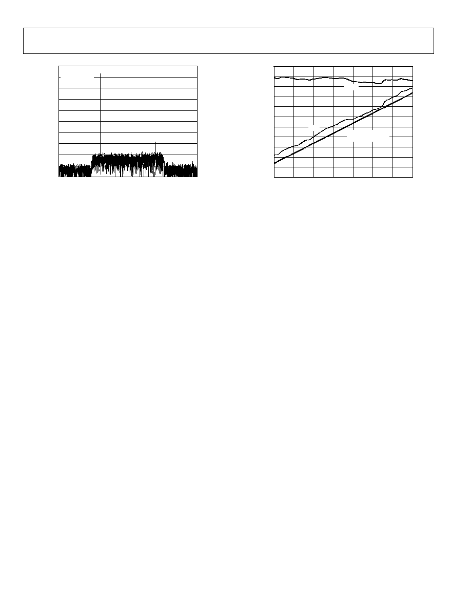
TYPICAL PERFORMANCE CHARACTERISTICS
76
70
S
NR (dB)
10
AIN FREQUENCY (MHz)
05156-073
75
74
73
72
71
30
50
70
90
110
130
150
170
190
25
°C
+25
°C
+85
°C
ENCODE = 92.16MSPS
AIN = 1dBFS
Figure 19. ADC Noise vs. Analog Frequency (46.08 MHz BW)
120
0
WORS
T CAS
E
S
P
URIOUS
(dBFS
a
nd dBc
)
0
90
ANALOG INPUT POWER LEVEL (dBFS)
05156-071
110
100
90
80
70
60
50
40
30
20
10
80
70
60
50
40
30
20
10
dBFS
dBc
SFDR = 90dB
REFERENCE LINE
ENCODE = 92.16MSPS
AIN = 37.7MHz
TEMPERATURE = 25
°C
Figure 20. Single Tone SFDR at 37.7 MHz
(dBFS
)
05156-064
15
0
30
45
60
75
90
105
120
135
150
1.25M
1.00M
750k
500k
500k
250k
0
250k
750k
1.00M
1.25M
FREQUENCY (Hz)
AIN = 1dBFS
SNR = 89dB (1.25MHz BW)
32k FFT
Figure 21. CDMA Single Tone AIN = 70 MHz; ENC = 92.16 MSPS
105
60
WORS
T CAS
E
HARMONIC (dBc
)
ANALOG INPUT FREQUENCY (MHz)
05156-074
100
95
90
85
80
75
70
65
WORST OTHER SPUR
HARMONICS
(SECOND, THIRD)
20
0
40
60
80
100
120
140
160
180
200
ENCODE = 92.16MSPS
AIN = 1dBFS
TEMPERATURE = 25
°C
Figure 22. Harmonics vs. Analog Frequency (IF)
110
0
W
O
R
S
T C
A
SE SPU
R
I
OU
S (
d
B
F
S and dB
c)
0
90
ANALOG INPUT POWER LEVEL (dBFS)
05156-072
100
90
80
70
60
50
40
30
20
10
80
70
60
50
40
30
20
10
dBFS
dBc
SFDR = 90dB
REFERENCE LINE
ENCODE = 92.16MSPS
AIN = 70MHz
TEMPERATURE = 25
°C
Figure 23. Single Tone SFDR at 70 MHz
(dBFS
)
05156-066
15
0
30
45
60
75
90
105
120
135
150
1.25M
1.00M
750k
500k
500k
250k
0
250k
750k
1.00M
1.25M
FREQUENCY (Hz)
32k FFT
Figure 24. CDMA Carrier AIN = 70 MHz; ENC = 92.16 MSPS
AD6654
Rev. 0 | Page 23 of 88
(dBFS
)
05156-065
15
0
30
45
60
75
90
105
120
135
150
1.25M
1.00M
750k
500k
500k
250k
0
250k
750k
1.00M
1.25M
FREQUENCY (Hz)
AIN = 1dBFS
SNR = 88dB (1.25MHz BW)
32k FFT
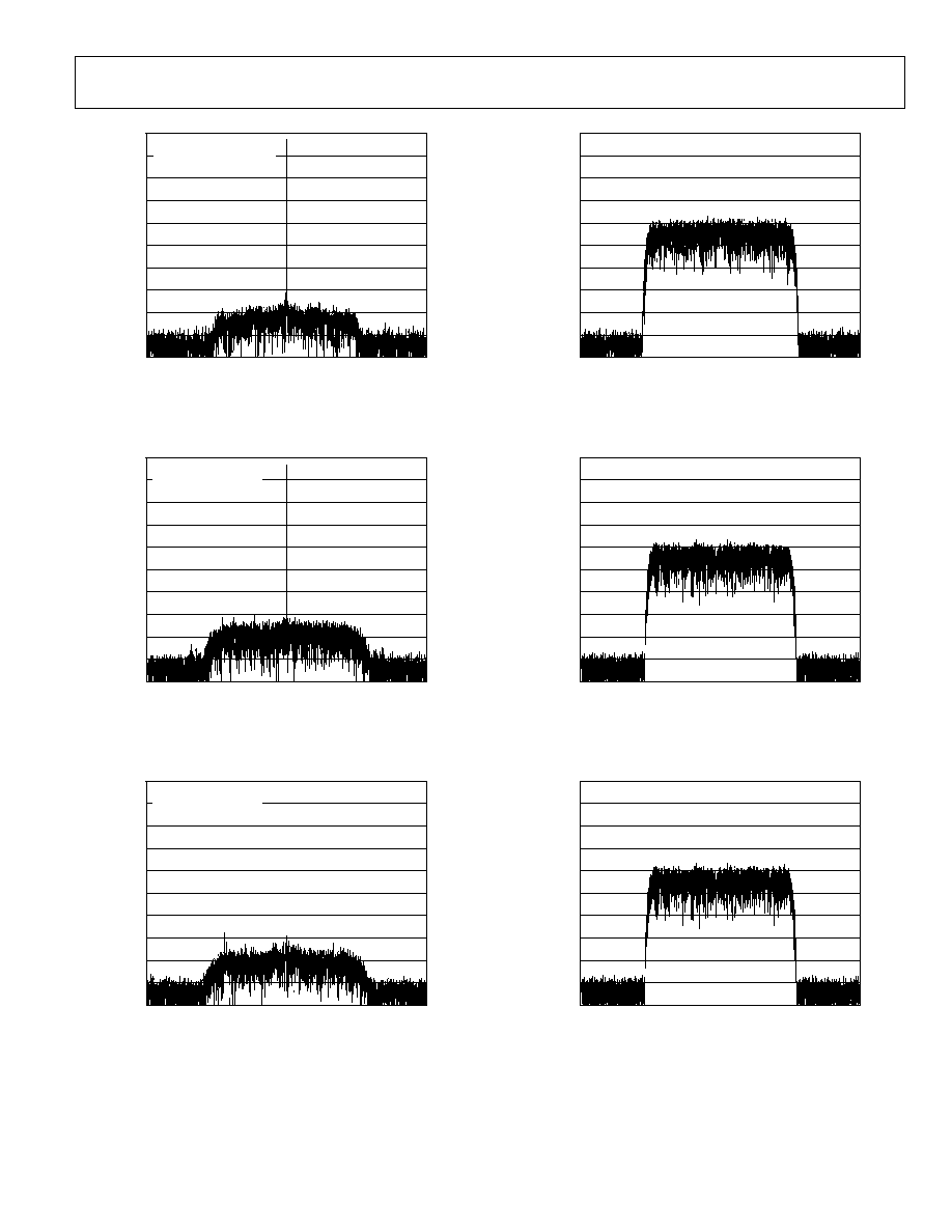
Figure 25. CDMA Single Tone AIN = 151.5 MHz; ENC = 92.16 MSPS
(dBFS
)
05156-067
15
0
30
45
60
75
90
105
120
135
150
3.5M
2.8M
2.1M
1.4M
1.4M
700k
0
700k
2.1M
2.8M
3.5M
FREQUENCY (Hz)
AIN = 1dBFS
SNR = 83dB (5MHz BW)
32k FFT
Figure 26. WCDMA Single Tone AIN = 70 MHz; Encode = 92.16 MSPS
(dBFS
)
05156-068
15
0
30
45
60
75
90
105
120
135
150
3.5M
2.8M
2.1M
1.4M
1.4M
700k
0
700k
2.1M
2.8M
3.5M
FREQUENCY (Hz)
AIN = 1dBFS
SNR = 82dB (5MHz BW)
32k FFT
Figure 27. WCDMA Single Tone AIN = 151.5 MHz; Encode = 92.16 MSPS
(dBFS
)
05156-083
15
0
30
45
60
75
90
105
120
135
150
1.25M
1.00M
750k
500k
500k
250k
0
250k
750k
1.00M
1.25M
FREQUENCY (Hz)
32k FFT
Figure 28. CDMA Carrier AIN = 151.5 MHz; ENC = 92.16 MSPS
(dBFS
)
05156-069
15
0
30
45
60
75
90
105
120
135
150
3.5M
2.8M
2.1M
1.4M
1.4M
700k
0
700k
2.1M
2.8M
3.5M
FREQUENCY (Hz)
32k FFT
Figure 29. WCDMA Carrier AIN = 70 MHz; Encode = 92.16 MSPS
(dBFS
)
05156-084
15
0
30
45
60
75
90
105
120
135
150
3.5M
2.8M
2.1M
1.4M
1.4M
700k
0
700k
2.1M
2.8M
3.5M
FREQUENCY (Hz)
32k FFT
Figure 30. WCDMA Carrier AIN = 151.5 MHz; Encode = 92.16 MSPS
AD6654
Rev. 0 | Page 24 of 88
(dBFS
)
05156-063
15
0
30
45
60
75
90
105
120
135
150
1.25M
1.00M
750k
500k
500k
250k
0
250k
750k
1.00M
1.25M
FREQUENCY (Hz)
F1
F2
AIN = 7dBFS
32k FFT
Figure 31. CDMA Two Tones at 55 MHz and 56 MHz; ENC = 92.16 MSPS
110
0
W
O
R
S
T C
A
SE SPU
R
I
OU
S (
d
B
F
S and dB
c)
7
77
INPUT POWER LEVEL (F1 = F2 (dBFS))
05156-070
100
90
80
70
60
50
40
30
20
10
67
57
47
37
27
17
SFDR = 90dB
REFERENCE LINE
dBFS
dBc
Figure 32. Two Tone SFDR at 55 MHz and 56 MHz
AD6654
Rev. 0 | Page 25 of 88
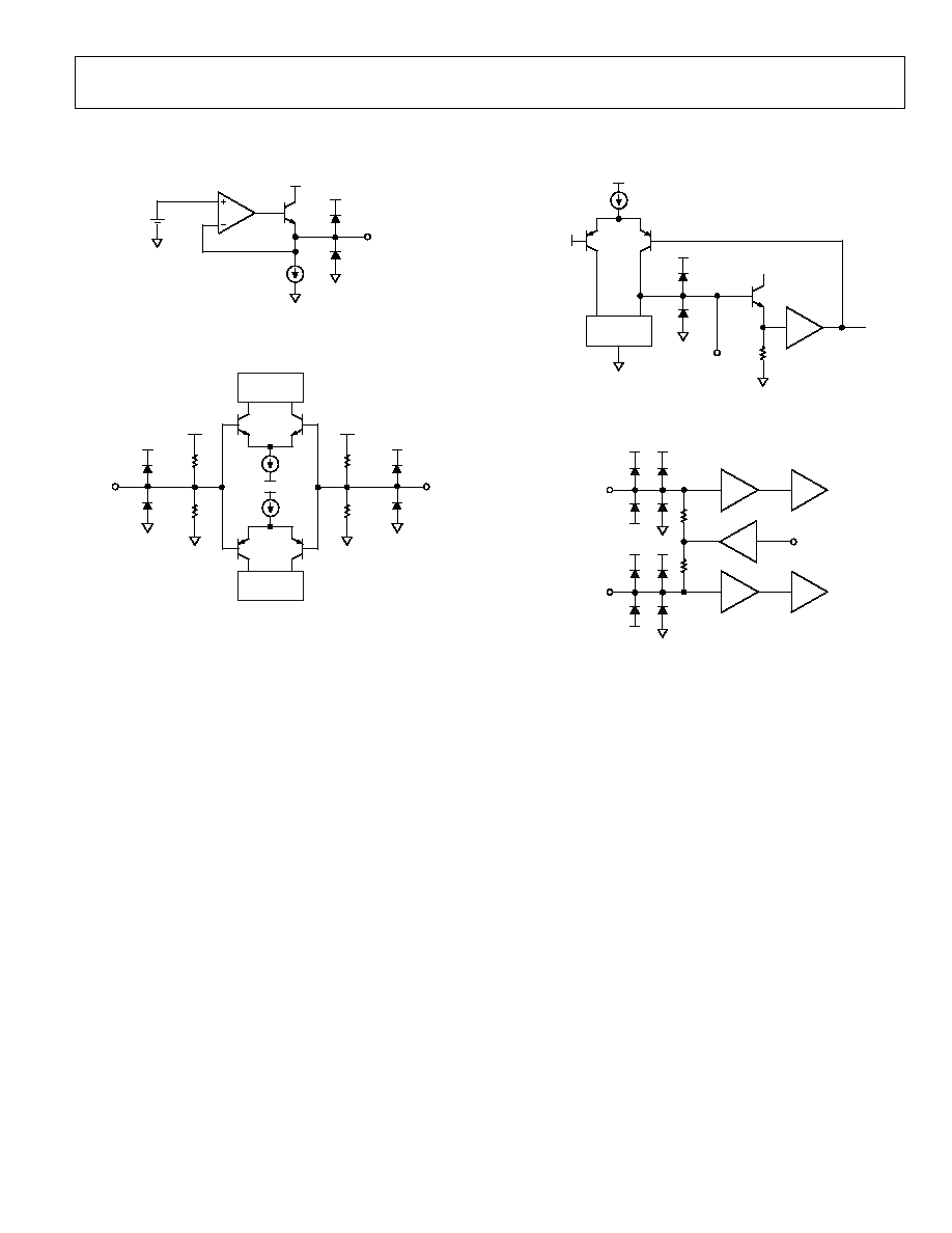
ADC EQUIVALENT CIRCUITS
AVDD
AVDD
V
REF
100
µA
2.4V
05156-023
Figure 33. ADC 2.4 V Reference
LOADS
LOADS
10k
10k
10k
10k
ENC
ENC+
AVDD
AVDD
AVDD
AVDD
05156-024
Figure 34. ADC Encode Inputs
AVDD
CURRENT
MIRROR
V
REF
AVDD
AVDD
C1, C2
05156-025
Figure 35. ADC Compensation Pins, C1 and C2
BUF
T/H
BUF
BUF
T/H
V
CH
AVDD
500
V
CL
AIN+
V
CH
AVDD
V
CL
AIN
500
V
REF
05156-026
Figure 36. ADC Analog Input Stage

AD6654
Rev. 0 | Page 26 of 88
TERMINOLOGY
Analog Bandwidth
The analog input frequency at which the spectral power of the
fundamental frequency (as determined by the FFT analysis) is
reduced by 3 dB.
Differential Analog Input Resistance,
Capacitance, and Impedance
The real and complex impedances measured at each analog
input port. The resistance is measured statically, and the
capacitance and differential input impedances are measured
with a network analyzer.
Differential Analog Input Voltage Range
The peak-to-peak differential voltage that must be applied to
the converter to generate a full-scale response. Peak differential
voltage is computed by observing the voltage on a single pin
and subtracting the voltage from the other pin, which is 180°
out of phase. Peak-to-peak differential is computed by rotating
the inputs phase 180° and taking the peak measurement again.
Then the difference is computed between both peak
measurements.
Encode Pulse Width/Duty Cycle
Pulse width high is the minimum amount of time that the
ENCODE pulse should be left in Logic 1 state to achieve the
rated performance. Pulse width low is the minimum time
ENCODE pulse should be left in the low state. Several internal
timing parameters are a function of t
ENCL
and t
ENCH
, optimum
performance will be achieved with 50/50 duty cycle.
Harmonic Distortion, Second
The ratio of the rms signal amplitude to the rms value of the
second harmonic component, reported in dBc.
Harmonic Distortion, Third
The ratio of the rms signal amplitude to the rms value of the
third harmonic component, reported in dBc.
Full-Scale Input Power
Expressed in dBm. Computed using the following equation:
=
001
.
0
log
10
2
INPUT
SCALE
FULL
SCALE
FULL
Z
V
Power
RMS
Minimum Conversion Rate
The encode rate at which the SNR of the lowest analog signal
frequency drops by no more than 3 dB below the guaranteed
limit.
Maximum Conversion Rate
Encode rate at which parametric testing is performed.
Noise for Any Range Within the ADC
-
-
×
=
10
dBFS
dBc
dBm
10
SIGNAL
SNR
FS
NOISE
Z
V
where Z is the input impedance, FS is the full scale of the device
for the frequency in question, SNR is the value for the particular
input level, and SIGNAL is the signal level within the ADC
reported in dB below full scale. This value includes both
thermal and quantization noise.
Power-Supply Rejection Ratio
The ratio of a change in input offset voltage to a change in
power-supply voltage.
Power-Supply Rise Time
The time from when the dc supply is initiated until the supply
output reaches the minimum specified operating voltage for the
AD6654, measured at the supply pin(s) of the AD6654.
Processing Gain
When the tuned channel occupies less bandwidth than the
input signal, this rejection of out-of-band noise is referred to as
processing gain. By using large decimation factors, processing
gain can improve the SNR of the ADC by 15 dB or more. Use
the following equation to estimate processing gain:
=
Bandwidth
Filter
Rate
Sample
Gain
Processing
_
2
/
_
log
10
_
Signal-to-Noise Ratio (Without Harmonics)
The ratio of the rms signal amplitude (set at 1 dB below full
scale) to the rms value of the sum of all other spectral
components, excluding the first five harmonics and dc.
Spurious-Free Dynamic Range (SFDR)
The ratio of the rms signal amplitude to the rms value of the
peak spurious spectral component. The peak spurious compo-
nent might, or might not be, a harmonic. SFDR can be reported
in dBc (degrades as signal level is lowered), or dBFS (always
related back to converter full scale).
Two-Tone Intermodulation Distortion Rejection
The ratio of the rms value of either input tone to the rms value
of the worst third-order intermodulation product, in dBc.
Two-Tone SFDR
Ratio of the rms value of either input tone to the rms value of
the peak spurious component. The peak spurious component
might, or might not be, an IMD product. SFDR can be reported
in dBc (degrades as signal level is lowered), or in dBFS (always
related back to converter full scale).
Worst Other Spur
Ratio of the rms signal amplitude to the rms value of the worst
spurious component (excluding the second and third harmonic)
reported in dBc.

AD6654
Rev. 0 | Page 27 of 88
THEORY OF OPERATION
ADC ARCHITECTURE
The AD6654 analog-to-digital converter (ADC) front end
employs a 3-stage subrange architecture. This design approach
achieves the required accuracy and speed, while maintaining
low power consumption.
The AD6654 front end has complementary analog input pins,
AIN+ and AIN-, as shown in Figure 1. Each analog input is
centered at 2.4 V and should swing ±0.55 V around this
reference (see Figure 36). Because AIN+ and AIN- are 180°
out of phase, the differential full-scale analog input signal is
2.2 V p-p.
Both analog inputs are buffered prior to the first track-and-
hold, TH1. The high state of the ENCODE pulse places TH1 in
hold mode. The held value of TH1 is applied to the input of a
5-bit coarse ADC1. The digital output of ADC1 drives a 5-bit
digital-to-analog converter, DAC1. DAC1 requires 14 bits of
precision that is achieved through laser trimming.
The output of DAC1 is subtracted from the delayed analog
signal at the input of TH3 to generate a first residue signal. TH2
provides an analog pipeline delay to compensate for the digital
delay of ADC1.
The first residue signal is applied to a second conversion stage
consisting of a 5-bit ADC2, 5-bit DAC2, and pipeline TH4. The
second DAC requires 10 bits of precision, which is met by the
process with no trim. The input to TH5 is a second residue
signal generated by subtracting the quantized output of DAC2
from the first residue signal held by TH4. TH5 drives a final
6-bit ADC3.
The digital outputs from ADC1, ADC2, and ADC3 are added
together and corrected in the digital error correction logic to
generate the final output data. The latency of the ADC core is
four CLK cycles. The resulting 14-bit ADC data is internally
routed directly to the integrated DDC for processing by the
4/6 independent DDC channels.
AD6654
Rev. 0 | Page 28 of 88
APPLICATION INFORMATION
ADC CONFIGURATION NOTES
Encoding the AD6654 ADC
The AD6654 encode signal must be a high quality, extremely
low phase noise source to prevent degradation of performance.
Maintaining 14-bit accuracy places a premium on encode clock
phase noise. SNR performance can easily degrade by 3 dB to
4 dB with 70 MHz analog input signals when using a high jitter
clock source. See the
AN-501
, Aperture Uncertainty and ADC
System Performance Application Note
, for details.
For optimum performance, the AD6654 ADC front end must
be clocked differentially. The encode signals are usually ac-
coupled into the ENC+ and ENC- pins via a transformer or
capacitors. The ENCODE pins are biased internally and require
no additional bias.
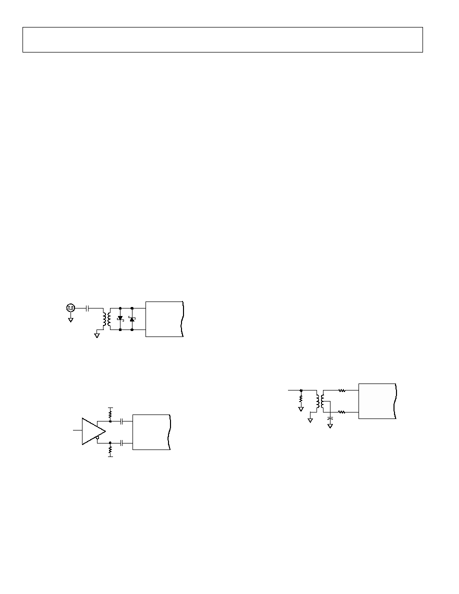
Figure 37 shows one preferred method for clocking the
AD6654. The clock source (low jitter) is converted from single-
ended to differential using an RF transformer. The back-to-back
Schottky diodes across the secondary of the transformer limit
clock excursions into the AD6654 to approximately 0.8 V p-p
differential. This helps prevent the large voltage swings of the
clock from feeding through to other portions of the AD6654,
and limits the noise presented to the encode inputs.
ENC+
ENC
0.1
µF
T1-4T
HSMS2812
DIODES
AD6654
CLOCK
SOURCE
05156-027
Figure 37. Crystal Clock Oscillator-Differential Encode
If a low jitter clock is available, another option is to ac-couple a
differential ECL/PECL signal to the encode input pins as shown
in Figure 38. A device that offers excellent jitter performance is
the MC100EL16 (or same family) from ON Semiconductor®.
ENC+
ENC
AD6654
VT
VT
0.1
µF
0.1
µF
ECL/
PECL
05156-028
Figure 38. Differential ECL for Encode
Driving the Analog Inputs
As with most high speed, high dynamic range ADCs, the analog
input to the AD6654 front end is differential. Differential inputs
improve on-chip performance, because signals are processed
through attenuation and gain stages. Most of the improvement
is a result of differential analog stages having high rejection of
even-order harmonics.
There are also benefits at the PCB level. First, differential inputs
have high common-mode rejection to stray signals such as
ground and power noise. Second, they provide good rejection to
common-mode signals such as local oscillator feed-through.
The AD6654 analog input pins, AIN+ and AIN-, are centered
at 2.4 V, and the signal at each input should swing ±0.55 V
around this voltage. Because AIN+ and AIN- are 180° out of
phase, the full-scale differential analog input signal is 2.2 V p-p.
Each analog input connects through a 500 resistor to the
2.4 V bias voltage and to the input of a differential buffer, as
shown in Figure 36. The resistor network on the input properly
biases the followers for maximum linearity and range.
Therefore, the analog source driving the AD6654 should be
ac-coupled to the input pins. Because the differential input
impedance of the AD6654 is 1 k, the analog input power
requirement is only -2 dBm, simplifying the driver amplifier in
many cases. To take full advantage of this high input
impedance, a 20:1 transformer is required. This is a large ratio
that could result in unsatisfactory performance. In this case, a
lower step-up ratio could be used. The recommended method
for driving the analog input of the AD6654 is to use a 4:1
impedance ratio RF transformer.
For example, if R
T
is set to 60.4 and R
S
is set to 25 , along
with a 4:1 impedance ratio transformer, the input matches to a
50 source with a full-scale drive of 4.8 dBm. Series resistors
(R
S
) on the secondary side of the transformer should be used to
isolate the transformer from A/D. This limits the amount of
dynamic current from the A/D flowing back into the secondary
of the transformer. The 50 impedance matching can also be
incorporated on the secondary side of the transformer, as
shown in the evaluation board schematic.
AIN
AIN+
ADT4-1WT
AD6654
ANALOG INPUT
SIGNAL
0.1
µF
R
T
R
S
R
S
05156-029
Figure 39. Transformer-Coupled Analog Input Circuit
In applications where dc-coupling, or additional gain is
required, use a differential output op amp from Analog Devices,
Inc., such as
AD8351
, to drive the AD6654 (Figure 40). The
AD8351
op amp can be driven differentially, or configured to
provide single-ended-to-differential conversion.
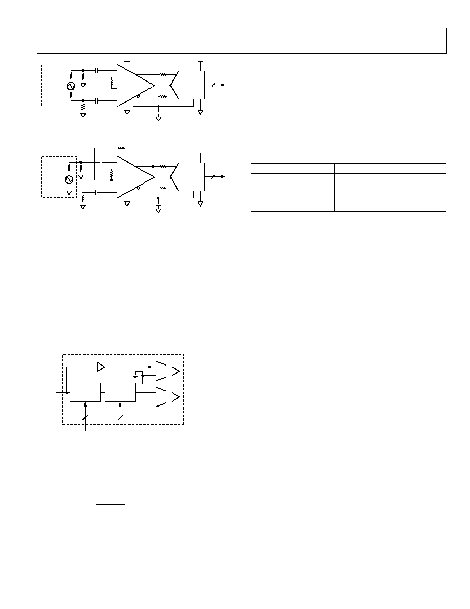
AD6654
Rev. 0 | Page 29 of 88
05156-030
BALANCE
50
SOURCE
25
100nF
25
100nF
AD8351
INHI
INLO
R
G
OPHI
OPLO
V
OCM
25
25
DIGITAL
OUT
AD6654
AIN+
AIN
V
REF
100nF
Figure 40. ADC Driving Application Using Differential Input
05156-062
SINGLE-
ENDED
50
SOURCE
R1
25
100nF
25
100nF
AD8351
INHI
INLO
R
G
OPHI
OPLO
V
OCM
25
25
DIGITAL
OUT
AD6654
AIN+
AIN
V
REF
100nF
R
F
Figure 41. ADC Driving Application Using Single-Ended Input
DDC CONFIGURATION NOTES
PLL Clock Multiplier
In the AD6654, the input clock rate must be the same as the
input data rate. In a typical digital down-converter architecture,
the clock rate is a limitation on the number of filter taps that
can be calculated in the programmable RAM coefficient filters
(MRCF, DRCF, and CRCF). For slower ADC clock rates (or for
any clock rate), this limitation can be overcome by using a PLL
clock multiplier to provide a higher clock rate to the RCF filters.
Using this clock multiplier, the internal signal processing clock
rate can be increased up to 200 MHz. The CLK signal is used as
an input to the PLL clock multiplier.
05156-031
CLK
PLL_CLK
ADC_CLK
DIVIDE BY N
(1, 2, 4 OR 8)
PLL CLOCK
MULTIPLIER
(4x TO 20x)
PLL CLOCK GENERATION
BYPASS_PLL
1 FOR BYPASS
N
M
2
5
0
1
1
0
Figure 42. PLL Clock Generation
The PLL clock multiplier is programmable and uses the input
clock rates between 30 MHz and 92.16 MHz to give a system
clock rate (output) of as high as 200 MHz.
The output clock rate is given by
N
M
CLK
CLK
PLL
×
=
_
where:
CLK
is the input port clock rate.
M
is a 5-bit programmable multiplication factor.
N
is a predivide factor and can be 1, 2, 4, or 8.
M
is a 5-bit number between 4 and 20 (inclusive).
The multiplication factor, M, is programmed using a 5-bit PLL
clock multiplier word in the ADC clock control register. A value
outside the valid range of 4 to 20 bypasses the PLL clock
multiplier and, therefore, the PLL clock is the same as the input
clock. The predivide factor, N, is programmed using a 2-bit
ADC pre-PLL clock divider word in the ADC clock control
register, as listed in Table 13.
Table 13. PLL Clock Generation Predivider Control
Predivide Word [1:0]
Divide-By Value for the Clock
00 Divide-by-1,
bypass
01 Divide-by-2
10 Divide-by-4
11 Divide-by-8
For best signal processing advantage, the user should program
the clock multiplier to give a system clock output as close as
possible to, but not exceeding, 200 MHz. The internal blocks of
the AD6654 that run off the PLL clock are rated to run at a
maximum of 200 MHz. The default power-up state for the PLL
clock multiplier is the bypass state, where CLK is passed on as
the PLL clock.
ADC Gain Control
The DDC input port has individual, high speed gain control
logic circuitry. Such gain control circuitry is useful in applica-
tions that involve large dynamic-range inputs. The AD6654 gain
control logic allows programmable upper and lower thresholds
and a programmable dwell-time counter for temporal
hysteresis.
The DDC input port has a 3-bit output from the gain control
block. The operation is controlled by the gain control enable bit
in the gain control register of the DDC input port. Logic 1 in
this bit programs the EXP[2:0] pins as gain control outputs.
Function
The gain control block features a programmable upper thresh-
old register and a lower threshold register. The ADC input data
is compared to both these registers. If ADC input data is larger
than the upper threshold register, then the gain control output
is decremented by 1. If the ADC input data is smaller than the
lower threshold register, then the gain control output is incre-
mented by 1.
When decrementing the gain control output, the change is
immediate. But when incrementing the output, a dwell-time
register is used to delay the change. If the ADC input is larger
than the upper threshold register value, the gain control output
is immediately decremented to prevent overflow.
When the ADC input is lower than the lower threshold register,
a dwell timer is loaded with the value in the programmable
20-bit dwell-time register. The counter decrements once every
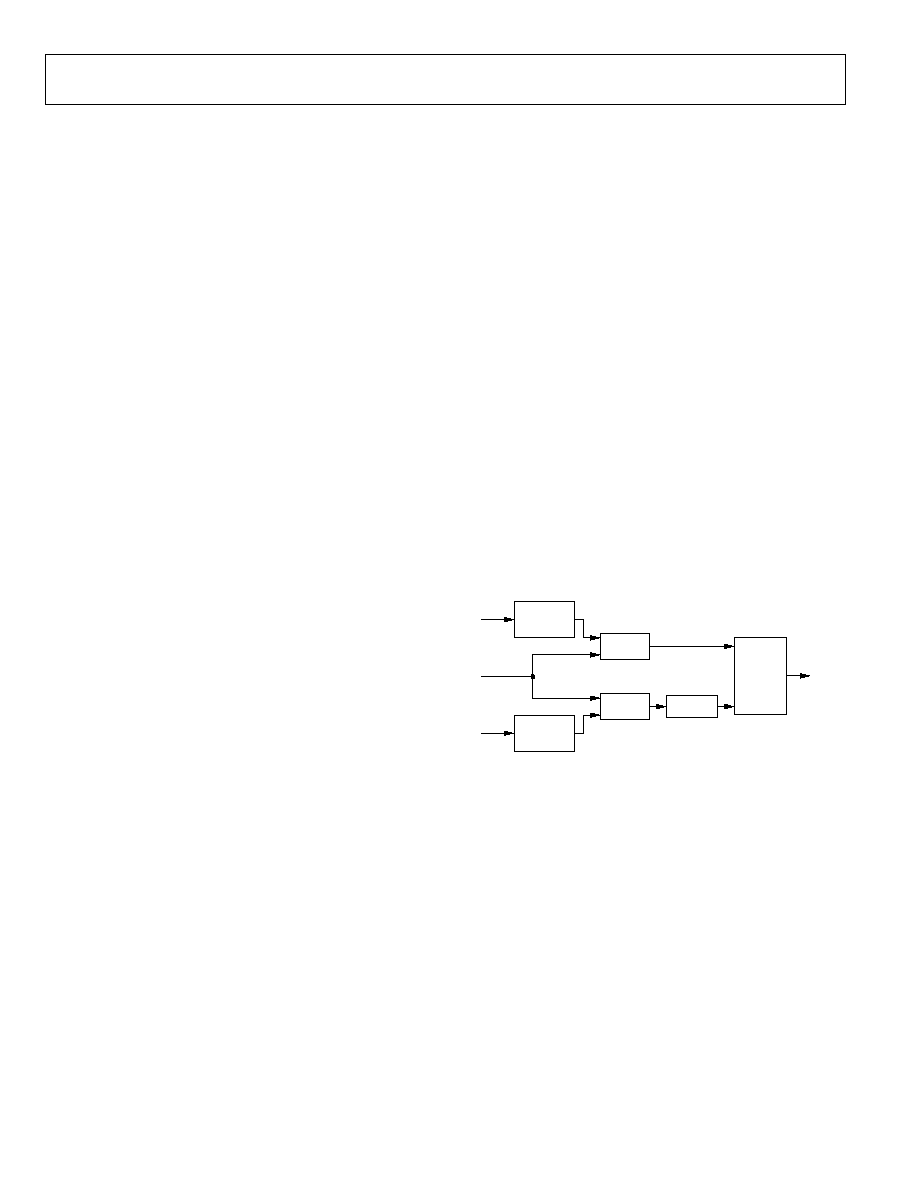
AD6654
Rev. 0 | Page 30 of 88
input clock cycle, as long as the input signal remains below the
lower threshold register value. If the counter reaches 1, the gain
control output is incremented by 1. If the signal goes above the
lower threshold register value, the gain adjustment is not made,
and the normal comparison to lower and upper threshold
registers is initiated once again. Therefore, the dwell timer
provides temporal hysteresis and prevents the gain from
continuously switching.
In a typical application, if the ADC signal goes below the lower
threshold for a time greater than the dwell time, then the gain
control output is incremented by 1. Gain control bits control the
gain ranging block, which appears before the ADC in the signal
chain. With each increment of the gain control output, gain in
the gain-ranging block is increased by 6.02 dB. This increases
the dynamic range of the input signal into the ADC by 6.02 dB.
This gain is compensated for in the AD6654 by relinearizing, as
explained in the Relinearization section. Therefore, the AD6654
can increase the dynamic range of the ADC by 42 dB, provided
that the gain-ranging block can support it.
Relinearization
The gain in the gain-ranging block (external) is compensated
for by relinearizing, using the exponent bits EXP[2:0] of the
input port. For this purpose, the gain control bits are connected
to the EXP[2:0] bits, providing an attenuation of 6.02 dB for
every increase in the gain control output. After the gain in the
external gain-ranging block and the attenuation in the AD6654
(using EXP bits), the signal gain is essentially unchanged. The
only change is the increase in the dynamic range of the ADC.
External gain-ranging blocks have a delay associated with
changing the gain of the signal. Typically, these delays can be
up to 14 clock cycles. The gain change in the AD6654 (via
EXP[2:0]) must be synchronized with the gain change in the
gain-ranging block (external). This is allowed in the AD6654 by
providing a flexible delay, programmable 6-bit word in the gain
control register. The value in this 6-bit word gives the delay in
input clock cycles. A programmable pipeline delay given by the
6-bit value (maximum delay of 63 clock cycles) is placed
between the gain control output and the EXP[2:0] input.
Therefore, the external gain-ranging block's settling delays
are compensated for in the AD6654.
Note that any gain changes that are initiated during the relinear-
ization period are ignored. For example, if the AD6654 detects
that a gain adjustment is required during the relinearization
period of a previous gain adjustment, then the new adjustment
is ignored.
Setting Up the Gain Control Block
To set up the gain control block for the input port, the individ-
ual upper threshold registers and lower threshold registers
should be written with appropriate values. The 10-bit values
written into upper and lower threshold registers are compared
to the 10 MSBs of the absolute magnitude calculated using the
input port data. The 20-bit dwell-time register should have the
appropriate number of clock cycles to provide temporal
hysteresis.
A 6-bit relinearization pipeline delay word is set to synchronize
with the settling delay in the external gain-ranging circuitry.
Finally, the gain control enable bit is written with Logic 1 to
activate the gain control block. On enabling, the gain control
output bits are made 000 (output on EXP[2:0] pins), which
represent the minimum gain for the external gain-ranging
circuitry and corresponding minimum attenuation during
relinearization. The normal functioning takes over, as explained
previously in this section.
05156-032
DWELL
TIMER
COMPARE
A
< B
DEC
INC
EXP GEN
FROM
MEMORY
MAP
EXP [2:0]
A
B
LOWER
THRESHOLD
REGISTER
COMPARE
A
> B
FROM
MEMORY
MAP
B
A
UPPER
THRESHOLD
REGISTER
FROM INPUT
PORTS
INCREASE
EXTERNAL GAIN
DECREASE
EXTERNAL GAIN
Figure 43. Gain Control Block Diagram

AD6654
Rev. 0 | Page 31 of 88
ADC INPUT PORT MONITOR FUNCTION
The AD6654 provides a power monitor function that can
monitor the DDC input stream and gather statistics about the
received signal in a signal chain. This function block can
operate in one of three modes measuring the following over a
programmable period of time:
· Peak power
· Mean power
· Number of samples crossing a threshold
These functions are controlled via the 2-bit power monitor
function select bits in the power monitor control register of the
DDC input port. The DDC input port can be set for different
modes, but only one function can be active at a time. The three
modes of operation can function continuously over a program-
mable time period. This time period is programmed as the
number of input clock cycles in a 24-bit ADC monitor period
register (AMPR). An internal magnitude storage register (MSR)
is used to monitor, accumulate, or count, depending on the
mode of operation.
PEAK DETECTOR MODE
Control Bits 00
The magnitude of the input port signal is monitored over a
programmable time period (given by AMPR) to give the peak
value detected. This mode is set by programming Logic 0 in the
power monitor function select bits in the power monitor
control register of the DDC input port. The 24-bit AMPR must
be programmed before activating this mode.
After enabling this mode, the value in the AMPR is loaded into
a monitor period timer and the countdown is started. The
magnitude of the input signal is compared to the MSR, and the
greater of the two is updated back into the MSR. The initial
value of the MSR is set to the current ADC input signal magni-
tude. This comparison continues until the monitor period timer
reaches a count of 1.
When the monitor period timer reaches a count of 1, the value
in the MSR is transferred to the power monitor holding register,
which can be read through the microport or the serial port. The
monitor period timer is reloaded with the value in the AMPR,
and the countdown is started. Also, the magnitude of the first
input sample is updated in the MSR, and the comparison and
update procedure, as explained above, continues. If the
interrupt is enabled, an interrupt is generated, and the interrupt
status register is updated when the AMPR reaches a count of 1.
Figure 44 is a block diagram of the peak detector logic. The
MSR contains the absolute magnitude of the peak detected by
the peak detector logic.
POWER MONITOR
HOLDING
REGISTER
MAGNITUDE
STORAGE
REGISTER
COMPARE
A
> B
TO
MEMORY
MAP
FROM
MEMORY
MAP
FROM
INPUT
PORTS
LOAD
CLEAR
LOAD
LOAD
05156-033
IS COUNT = 1?
DOWN
COUNTER
TO
INTERRUPT
CONTROLLER
POWER MONITOR
PERIOD REGISTER
Figure 44. ADC Input Peak Detector Block Diagram
MEAN POWER MODE
Control Bits 01
In this mode, the magnitude of the input port signal is
integrated (by adding an accumulator) over a programmable
time period (given by AMPR) to give the integrated magnitude
of the input signal. This mode is set by programming Logic 1 in
the power monitor function select bits in the power monitor
control register of the DDC input port. The 24-bit AMPR,
representing the period over which integration is performed,
must be programmed before activating this mode.
After enabling this mode, the value in the AMPR is loaded into
a monitor period timer, and the countdown is immediately
started. The 15-bit magnitude of input signal is right-shifted by
nine bits to give 6-bit data. This 6-bit data is added to the
contents of a 24-bit holding register, thereby performing an
accumulation. The integration continues until the monitor
period timer reaches a count of 1.
When the monitor period timer reaches a count of 1, the value
in the MSR is transferred to the power monitor holding register
(after some formatting), which can be read through the micro-
port or the serial port. The monitor period timer is reloaded
with the value in the AMPR, and the countdown is started.
Also, the first input sample signal magnitude is updated in the
MSR, and the accumulation continues with the subsequent
input samples. If the interrupt is enabled, an interrupt is
generated, and the interrupt status register is updated when the
AMPR reaches a count of 1. Figure 45 illustrates the mean
power monitoring logic.
The value in the MSR is a floating-point number with 4 MSBs
and 20 LSBs. If the 4 MSBs are EXP and the 20 LSBs are MAG,
the value in dBFS can be decoded using the following equation:
(
)
-
-
=
1
2
2
log
10
20
EXP
MAG
MeanPower
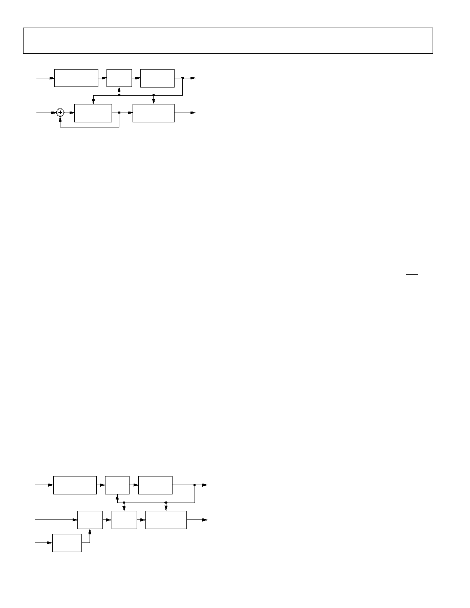
AD6654
Rev. 0 | Page 32 of 88
05156-
034
POWER MONITOR
HOLDING
REGISTER
ACCUMULATOR
TO
MEMORY
MAP
FROM
MEMORY
MAP
FROM
INPUT
PORTS
LOAD
CLEAR
LOAD
IS COUNT = 1?
DOWN
COUNTER
TO
INTERRUPT
CONTROLLER
POWER MONITOR
PERIOD REGISTER
Figure 45. ADC Input Mean Power Monitoring Block Diagram
THRESHOLD CROSSING MODE
Control Bits 10
In this mode of operation, the magnitude of the input port
signal is monitored over a programmable time period (given
by AMPR) to count the number of times it crosses a certain
programmable threshold value. This mode is set by program-
ming Logic 1x (where x is a don't care bit) in the power monitor
function select bits in the power monitor control register of the
DDC input port. Before activating this mode, the user needs to
program the 24-bit AMPR and the 10-bit upper threshold register
of the DDC input port. The same upper threshold register is
used for both power monitoring and gain control (see the ADC
Gain Control section).
After entering this mode, the value in the AMPR is loaded into
a monitor period timer, and the countdown is started. The
magnitude of the input signal is compared to the upper
threshold register (programmed previously) on each input clock
cycle. If the input signal has a magnitude greater than the upper
threshold register, then the MSR register is incremented by 1.
The initial value of the MSR is set to 0. This comparison and
incrementing of the MSR register continues until the monitor
period timer reaches a count of 1.
When the monitor period timer reaches a count of 1, the value
in the MSR is transferred to the power monitor holding register,
which can be read through the microport or the serial port. The
monitor period timer is reloaded with the value in the AMPR,
and the countdown is started. The MSR register is also cleared
to a value of 0. If interrupts are enabled, an interrupt is gener-
ated, and the interrupt status register is updated when the
AMPR reaches a count of 1. Figure 46 illustrates the threshold
crossing logic. The value in the MSR is the number of samples
that have an amplitude greater than the threshold register.
05156-
035
POWER MONITOR
HOLDING
REGISTER
COMPARE
A
> B
UPPER
THRESHOLD
REGISTER
COMPARE
A
> B
TO
MEMORY
MAP
FROM
MEMORY
MAP
FROM
MEMORY
MAP
FROM
INPUT
PORTS
LOAD
CLEAR
LOAD
IS COUNT = 1?
DOWN
COUNTER
TO
INTERRUPT
CONTROLLER
POWER MONITOR
PERIOD REGISTER
B
A
Figure 46. ADC Input Threshold Crossing Block Diagram
ADDITIONAL CONTROL BITS
For additional flexibility in the power monitoring process, two
control bits are provided in the power monitor control register.
The two control bits are the disable monitor period timer bit
and the clear-on-read bit. These options have the same function
in all three modes of operation.
Disable Monitor Period Timer Bit
When the disable monitor period timer bit is written with
Logic 1, the timer continues to run but does not cause the
contents of the MSR to be transferred to the holding register
when the count reaches 1. This function of transferring the
MSR to the power monitor holding register and resetting the
MSR is now controlled by a read operation on the microport or
serial port.
When a microport or serial port read is performed on the
power monitor holding register, the MSR value is transferred to
the holding register. After the read operation, the timer is
reloaded with the AMPR value. If the timer reaches 1 before the
microport or serial port read, the MSR value is not transferred
to the holding register, as in normal operation. The timer still
generates an interrupt on the AD6654 interrupt pin and updates
the interrupt status register. An interrupt appears on the IRP
pin, if interrupts are enabled in the interrupt enable register.
Clear-on-Read Bit
This control bit is valid only when the disable monitor period
timer bit is Logic 1. When both of these bits are set, a read
operation to either the microport or the serial port reads the
MSR value, and the monitor period timer is reloaded with the
AMPR value. The MSR is cleared (written with current input
signal magnitude in peak power and mean power modes;
written with a 0 in threshold crossing mode), and normal
operation continues.
When the monitor period timer is disabled and the clear-on-
read bit is set, a read operation to the power monitor holding
register clears the contents of the MSR and, therefore, the power
monitor loop restarts.
If the clear-on-read bit is Logic 0, the read operation to the
microport or serial port does not clear the MSR value after it is
transferred into the holding register. The value from the
previous monitor time period persists, and it continues to be
compared, accumulated, or incremented, based on new input
signal magnitude values.

AD6654
Rev. 0 | Page 33 of 88
INPUT CROSSBAR MATRIX
The AD6654 has one ADC input port and six channels. Each
channel can individually select its input source from either the
real ADC input port, or from an internally generated pseudo
random sequence (referred to as a PN sequence) generator.
Each channel has an input crossbar matrix to facilitate selection
of the input signal source.
The selection of input signal for a particular channel is made
using a 4-bit cross bar mux select word in the ADC input
control register.
Each channel has a separate selection for individual control.
Cross bar mux selection enables each channel to select its input
signal source.
Table 14 gives the valid combinations of cross bar mux select
values and the corresponding input signal selections.
Table 14. Cross Bar Mux Selection Bits
Cross Bar Mux Select Bits
Input Signal Selection
0010
ADC input drives the channel.
0100
Internal PN sequence drives the
channel.

AD6654
Rev. 0 | Page 34 of 88
NUMERICALLY CONTROLLED OSCILLATOR (NCO)
Each channel consists of an independent complex NCO and a
complex mixer. This processing stage is comprised of a digital
tuner consisting of three multipliers and a 32-bit complex NCO.
The NCO serves as a quadrature local oscillator capable of
producing an NCO frequency of between CLK/2 and +CLK/2
with a resolution of CLK/232 in the complex mode, where CLK
is the input clock frequency.
The frequency word used for generating the NCO is a 32-bit
word. This word is used to generate a 20-bit phase word. A
16-bit phase offset word is added to this phase word. 18 bits of
this phase word are used to generate the sine and cosine of the
required NCO frequency. The amplitude of the sine and cosine
are represented using 17 bits. The worst-case spurious signal
from the NCO is better than -100 dBc for all output
frequencies.
Because all the filtering in the AD6654 is low-pass filtering, the
carrier of interest is tuned down to dc (frequency = 0 Hz). This
is illustrated in Figure 47. Once the signal of interest is tuned
down to dc, the unwanted adjacent carriers can be rejected
using the low-pass filtering that follows.
NCO FREQUENCY
The NCO frequency value is given by the 32-bit twos comple-
ment number entered in the NCO frequency register.
Frequencies between -CLK/2 and +CLK/2 (with +CLK/2
excluded) are represented using this frequency word:
0x8000 0000 represents a frequency given by -CLK/2.
0x0000 0000 represents dc (frequency is 0 Hz).
0x7FFF FFFF represents CLK/2 - CLK/2
32
.
The NCO frequency word can be calculated using following the
equation:
(
)
CLK
CLK
CH
f
f
f
FREQ
NCO
,
mod
2
_
32
=
where:
NCO_FREQ
is the 32-bit twos complement number represent-
ing the NCO frequency register.
f
CH
is the desired carrier frequency.
f
CLK
is the clock rate for the channel under consideration.
mod( ) is a remainder function. For example, mod(110, 100) =
10 and, for negative numbers, mod(-32, 10) = -2.
Note that this equation applies to the aliasing of signals in the
digital domain (that is, aliasing introduced when digitizing
analog signals).
For example, if the carrier frequency is 100 MHz and the clock
frequency is 80 MHz,
(
)
25
.
0
80
20
,
mod
=
=
CLK
DK
CH
f
f
f
This, in turn, converts to 0x4000 0000 in the 32-bit twos
complement representation for NCO_FREQ.
05156-036
NCO TUNES SIGNAL TO
SIGNAL OF INTEREST
AFTER FREQUENCY TRANSLATION
SIGNAL OF INTEREST
SIGNAL OF INTEREST IMAGE
SIGNAL OF INTEREST IMAGE
fs/2
7fs/16
3fs/8
5fs/16
fs/4
3fs/16
fs/8
fs/16
DC
fs/16
fs/8
3fs/16
fs/4
5fs/16
3fs/8
7fs/16
fs/2
fs/2
7fs/16
3fs/8
5fs/16
fs/4
3fs/16
fs/8
fs/16
DC
fs/16
fs/8
3fs/16
fs/4
5fs/16
3fs/8
7fs/16
fs/2
FREQUENCY TRANSLATION (SINGLE 1MHz CHANNEL TUNED TO BASEBAND)
WIDEBAND INPUT SPECTRUM (30MHz FROM HIGH SPEED ADC)
WIDEBAND INPUT SPECTRUM (fsample/2
TO +
fsample/2)
Figure 47. Frequency Translation Principle Using the NCO and Mixer

AD6654
Rev. 0 | Page 35 of 88
If the carrier frequency is 70 MHz and the clock frequency is
80 MHz, then:
125
.
0
80
10
)
,
mod(
=
=
CLK
CLK
CH
f
f
f
This, in turn, converts to 0xE000 0000 in the twos complement
32-bit representation.
MIXER
The NCO is accompanied by a mixer. Its operation is similar to
an analog mixer. It performs the down-conversion of real input
signals by using the NCO frequency as a local oscillator. This
mixer performs a real mixer operation (with two multipliers).
The mixer adjusts its operation based on the input signal
provided to each individual channel.
BYPASS
The NCO and the mixer can be individually bypassed in each
channel by writing Logic 1 in the NCO bypass bit in the NCO
control register of the channel under consideration.
CLEAR PHASE ACCUMULATOR ON HOP
When clear, the NCO accumulator bit of the NCO control
register is set (Logic 1), the NCO phase accumulator is cleared
prior to a frequency hop. Refer to the Chip Synchronization
section for details on frequency hopping. This ensures a
consistent phase of the NCO on each hop. The NCO phase
offset is unaffected by this setting and is still in effect. If phase-
continuous hopping is needed, this bit should be cleared (NCO
accumulator is not cleared). The last phase in the NCO phase
register is the initiating point for the new frequency.
PHASE DITHER
The AD6654 provides a phase dither option for improving the
spurious performance of the NCO. Writing Logic 1 in the phase
dither enable bit of the NCO control register of individual
channels enables phase dither. When phase dither is enabled,
random phase is added to the LSBs of the phase accumulator of
the NCO. When phase dither is enabled, spurs due to phase
truncation in the NCO are randomized.
The energy from these spurs is spread into the noise floor and
the spurious free dynamic range is increased at the expense of a
very slight decrease in the SNR. The choice of whether to use
phase dither in a system is ultimately decided by the system
goals. If lower spurs are desired at the expense of a slightly
raised noise floor, phase dither should be employed. If a low
noise floor is desired and higher spurs can be tolerated or
filtered by subsequent stages, then phase dither is not needed.
AMPLITUDE DITHER
Amplitude dither can be used to improve spurious performance
of the NCO. Amplitude dither is enabled by writing Logic 1 in
the amplitude dither enable bit of the NCO control register of
the channel under consideration. Random amplitude is added
to the LSBs of the sine and cosine amplitudes, when this feature
is enabled. Amplitude dither improves performance by random-
izing the amplitude quantization errors within the angular-to-
Cartesian conversion of the NCO. This option might reduce
spurs at the expense of a slightly raised noise floor. Amplitude
dither and phase dither can be used together, separately, or not
at all.
NCO FREQUENCY HOLD-OFF REGISTER
When the NCO frequency registers are written by the micro-
port or serial port, data is passed to a shadow register. Data can
be moved to the main registers when the channel comes out of
sleep mode, or when a sync hop occurs. In either event, a
counter can be loaded with the NCO frequency hold-off
register value. The 16-bit unsigned integer counter starts
counting down, clocked by the input port clock selected at the
crossbar mux. When the counter reaches 0, the new frequency
value in the shadow register is written to the NCO frequency
register. Writing 1 in this hold-off register updates the NCO
frequency register as soon as the start sync or hop sync occurs.
See the Chip Synchronization section for details.
PHASE OFFSET
The phase offset register can be written with a value that is
added as an offset to the phase accumulator of the NCO. This
16-bit register is interpreted as a 16-bit unsigned integer. A
0x0000 in this register corresponds to a 0 radian offset and a
0xFFFF corresponds to an offset of 2 × (1 - 1/2
16
) radians.
This register allows multiple NCOs (multiple channels) to be
synchronized to produce complex sinusoids with a known and
steady phase difference.
HOP SYNC
A hop sync should be issued to the channel, when the NCO
frequency of that channel needs to be changed from one
frequency to another. See the Chip Synchronization section for
details.
AD6654
Rev. 0 | Page 36 of 88
FIFTH-ORDER CIC FILTER
The signal processing stage immediately after the NCO is a CIC
filter stage. This stage implements a fixed coefficient, decimat-
ing, cascade integrated comb filter. The input rate to this filter is
the same as the data rate at the input port; the output rate from
this stage is dependent on the decimation factor.
CIC
IN
CIC
M
f
f
=
The decimation ratio, M
CIC
, can be programmed from 2 to 32
(only integer values). The 5-bit word in the CIC decimation
register is used to set the CIC decimation factor. A binary value
of one less than the decimation factor is written into this
register. The decimation ratio of 1 can be achieved by bypassing
the CIC filter stage. The frequency response of the filter is given
by the following equations. The gain and pass-band droop of
the CIC should be calculated by these equations. Both parame-
ters can be offset in the RCF stage.
(
)
5
1
5
1
1
2
1
)
(
-
-
×
=
-
-
+
Z
Z
z
H
CIC
CIC
M
S
5
)
5
(
2
1
)
(
×
=
×
+
IN
IN
f
CIC
S
f
f
SIN
f
M
SIN
f
H
CIC
where:
f
IN
is the data input rate to the channel under consideration.
S
CIC
, the scale factor, is a programmable unsigned integer
between 0 and 20.
The attenuation of the data into the CIC stage should be con-
trolled in 6 dB increments. For the best dynamic range, S
CIC
should be set to the smallest value possible (lowest attenuation
possible) without creating an overflow condition. This can be
accomplished safely using the following equation, where
input_level is the largest possible fraction of the full-scale value
at the input port. This value is output from the NCO stage and
pipelined into the CIC filter.
(
)
(
)
5
_
log
5
2
-
×
=
level
input
M
ceil
S
CIC
CIC
(
)
level
input
M
OL
CIC
S
CIC
CIC
_
2
5
5
×
=
+
BYPASS
The fifth-order CIC filter can be bypassed when no decimation
is required of it. When it is bypassed, the scaling operation is
not performed. In bypass mode, the output of the CIC filter is
the same as the input of the CIC filter.
CIC REJECTION
Table 15 illustrates the amount of bandwidth as a percentage of
the data rate into the CIC stage, which can be protected with
various decimation rates and alias rejection specifications. The
maximum input rate into the CIC is 150 MHz (the same as the
maximum input port data rate). The data can be scaled to any
other allowable sample rate.
Table 15 can be used to decide the minimum decimation
required in the CIC stage to preserve a certain bandwidth. The
CIC5 stage can protect a much wider bandwidth to any given
rejection, when a decimation ratio lower than that identified in
the table is used. The table helps to calculate an upper boundary
on decimation, M
CIC
, given the desired filter characteristics.
Table 15. SSB CIC5 Alias Rejection Table (f
IN
= 1)
MCIC5
-60 dB
-70 dB
-80 dB
-90 dB
-100 dB
2
8.078
6.393
5.066
4.008
3.183
3
6.367
5.110
4.107
3.297
2.642
4
5.022
4.057
3.271
2.636
2.121
5
4.107
3.326
2.687
2.170
1.748
6
3.463
2.808
2.270
1.836
1.480
7
2.989
2.425
1.962
1.588
1.281
8
2.627
2.133
1.726
1.397
1.128
9
2.342
1.902
1.540
1.247
1.007
10
2.113
1.716
1.390
1.125
0.909
11
1.924
1.563
1.266
1.025
0.828
12
1.765
1.435
1.162
0.941
0.760
13
1.631
1.326
1.074
0.870
0.703
14
1.516
1.232
0.998
0.809
0.653
15
1.416
1.151
0.932
0.755
0.610
16
1.328
1.079
0.874
0.708
0.572
17
1.250
1.016
0.823
0.667
0.539
18
1.181
0.960
0.778
0.630
0.509
19
1.119
0.910
0.737
0.597
0.483
20
1.064
0.865
0.701
0.568
0.459
21
1.013
0.824
0.667
0.541
0.437
22
0.967
0.786
0.637
0.516
0.417
23
0.925
0.752
0.610
0.494
0.399
24
0.887
0.721
0.584
0.474
0.383
25
0.852
0.692
0.561
0.455
0.367
26
0.819
0.666
0.540
0.437
0.353
27
0.789
0.641
0.520
0.421
0.340
28
0.761
0.618
0.501
0.406
0.328
29
0.734
0.597
0.484
0.392
0.317
30
0.710
0.577
0.468
0.379
0.306
31
0.687
0.559
0.453
0.367
0.297
32
0.666
0.541
0.439
0.355
0.287

AD6654
Rev. 0 | Page 37 of 88
EXAMPLE CALCULATIONS
Goal: Implement a filter with an input sample rate of 100 MHz
requiring 100 dB of alias rejection for a ±1.4 MHz pass band.
Solution: First determine the percentage of the sample rate that
is represented by the pass band.
4
.
1
MHz
100
MHz
4
.
1
100
=
×
=
FRACTION
BW
In the -100 dB column in Table 15, find the value greater than
or equal to the pass-band percentage of the clock rate. Then
find the corresponding rate decimation factor (M
CIC
). For an
M
CIC
of 6, the frequency that has -100 dB of alias rejection is
1.48%, which is slightly larger than the 1.4% calculated.
Therefore, for this example, the maximum bound on CIC
decimation rate is 6. A higher M
CIC
means less alias rejection
than the 100 dB required.
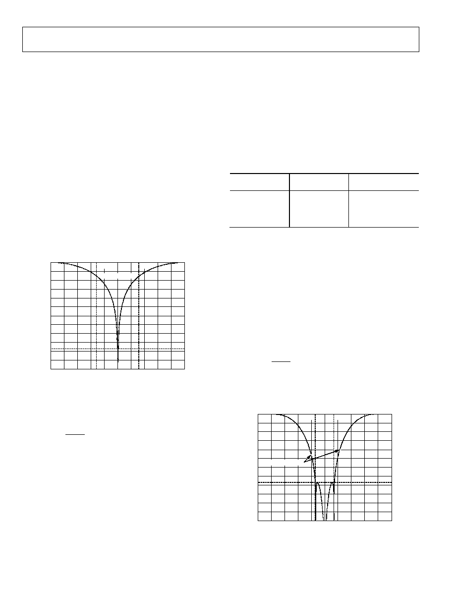
AD6654
Rev. 0 | Page 38 of 88
FIR HALF-BAND BLOCK
The output of the CIC filter is pipelined into the FIR HB (half-
band) block. Each channel has two sets of cascading fixed
coefficient FIR and fixed coefficient half-band filters. The half-
band filters decimate by 2. Each of these filters (FIR1, HB1,
FIR2, and HB2) is described in the following sections.
3-TAP FIXED COEFFICIENT FILTER (FIR1)
The 3-tap FIR filter is useful in certain filter configurations in
which extra alias protection is needed for the decimating HB1
filter. It is a simple sum-of-products FIR filter with three filter
taps and 2-bit fixed coefficients. Note that this filter does not
decimate. The coefficients of this symmetric filter are {1, 2, 1}.
The normalized coefficients used in the implementation are
{0.25, 0.5, 0.25}.
The user can either use or bypass this filter. Writing Logic 0 to
the FIR1 enable bit in the FIR-HB control register bypasses this
fixed coefficient filter. The filter is useful only in certain filter
configurations and bypassing it for other applications results in
power savings.
05156-037
FRACTION OF FIR1 INPUT SAMPLE RATE
0
0.1
0.2
0.3
0.4
0.5
0.6
0.7
0.8
0.9
dBc
0
16.67
8.33
33.33
25.00
50.00
41.67
66.67
58.33
83.33
75.00
100.00
91.67
0.34
0.66
81
FIR1 RESPONSE
Figure 48. FIR1 Filter Response to the Input Rate of the Filter
This filter runs at the same sample rate as the CIC filter output
rate and is given by
CIC
IN
FIR1
M
f
f
=
where:
f
IN
is the input rate to the channel.
M
CIC
is the decimation ratio in the CIC filter stage.
The maximum input and output rates for this filter are
150 MHz.
DECIMATE-BY-2 HALF-BAND FILTER (HB1)
The next stage of the FIR-HB block is a decimate-by-2 half-
band filter. The 11-tap, symmetrical, fixed coefficient HB1 filter
has low power consumption due to its polyphase implementa-
tion. The filter has 22 bits of input and output data with 10-bit
coefficients. Table 16 lists the coefficients of the half-band filter.
The normalized coefficients used in the implementation and
the 10-bit decimal equivalent value of the coefficients are also
listed. Other coefficients are 0s.
Table 16. Fixed Coefficients for HB1 Filter
Coefficient
Number
Normalized
Coefficient
Decimal Coefficient
(10-Bit)
C1, C11
0.013671875
7
C3, C9
-0.103515625
-53
C5, C7
0.58984375
302
C6 1 512
Similar to the FIR1 filter, this filter can be used or bypassed.
Writing Logic 0 to the HB1 enable bit in the FIR-HB control
register bypasses this fixed coefficient HB filter. The filter is
useful only in certain filter configurations and bypassing it for
other applications results in power savings. For example, it is
useful in narrow-band and wideband output applications in
which more filtering is required, as compared to very wide
bandwidth applications in which a higher output rate might
prohibit the use of a decimating filter. The response of the filter
is shown in Figure 49.
The input sample rate of this filter is the same as the CIC filter
output rate and is given by
CIC
IN
HB1
M
f
f
=
where:
f
IN
is the input rate to the channel.
M
CIC
is the decimation ratio in the CIC filter stage.
05156-038
FRACTION OF HB1 INPUT SAMPLE RATE
0
0.1
0.2
0.3
0.4
0.5
0.6
0.7
0.8
0.9
dBc
0
20
10
40
30
60
50
80
70
110
100
90
120
HB1 RESPONSE
0.43
0.57
77
Figure 49. HB1 Filter Response to the Input Rate of the Filter
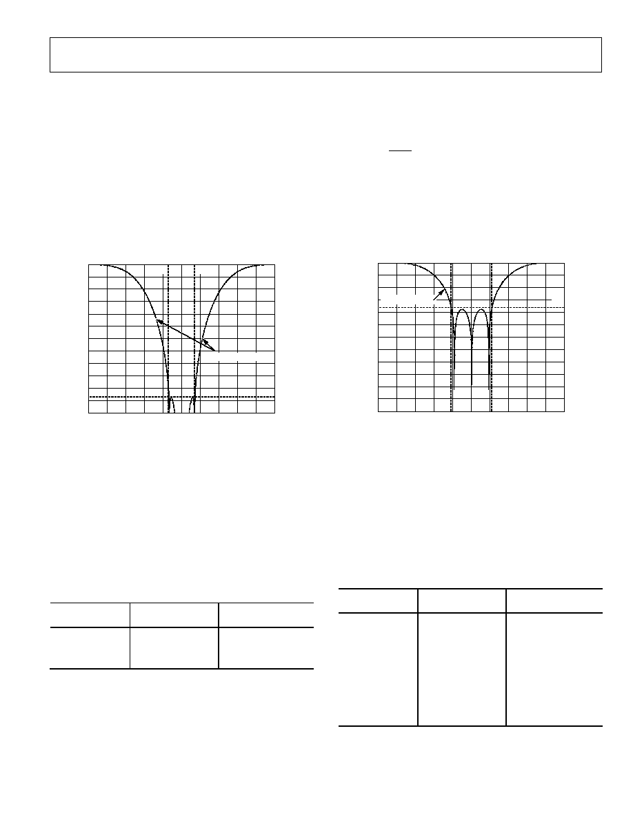
AD6654
Rev. 0 | Page 39 of 88
The filter has a maximum input sample rate of 150 MHz and,
when filter is not bypassed, the maximum output rate is
75 MHz.
The filter has a ripple of 0.0012 dB and rejection of 77 dB. For
an alias rejection of 77 dB, the alias-protected bandwidth is 14%
of the filter input sample rate. The bandwidth of the filter for a
ripple of 0.00075 dB is also the same as the alias-protected
bandwidth, due to the nature of half-band filters. The 3 dB
bandwidth of this filter is 44% of the filter input sample rate.
For example, if the sample rate into the filter is 50 MHz, then
the alias-protected bandwidth of the HB1 filter is 7 MHz. If the
bandwidth of the required carrier is greater than 7 MHz, then
HB1 might not be useful.
05156-039
FRACTION OF HB1 INPUT SAMPLE RATE
0
0.1
0.2
0.3
0.4
0.5
0.6
0.7
0.8
0.9
dBc
0
20
10
40
30
60
50
80
70
100
90
120
110
107
FIR1 + HB1 RESPONSE
0.43
0.57
Figure 50. Composite Response of FIR1 and HB1 Filters to Their Input Rate
6-TAP FIXED COEFFICIENT FILTER (FIR2)
Following the first cascade of the FIR1 and HB1 filters is the
second cascade of the FIR2 and HB2 filters. The 6-tap, fixed
coefficient FIR2 filter is useful in providing extra alias
protection for the decimating HB2 filter in certain filter
configurations. It is a simple sum-of-products FIR filter with
six filter taps and 5-bit fixed coefficients. Note that this filter
does not decimate. The normalized coefficients used in the
implementation and the 5-bit decimal equivalent value of the
coefficients are listed in Table 17.
Table 17. 6-Tap FIR2 Filter Coefficients
Coefficient
Number
Normalized
Coefficient
Decimal Coefficient
(5-Bit)
C0, C5
-0.125
-2
C1, C4
0.1875
3
C2, C3
0.9375
15
The user can either use or bypass this filter. Writing Logic 0 to
FIR2 enable bit in the FIR-HB control register bypasses this
fixed coefficient filter. The filter is useful only in certain filter
configurations and bypassing it for other applications results in
power savings. The filter is especially useful in increasing the
stop-band attenuation of the HB2 filter that follows. Therefore,
it is optimal to use both FIR2 and HB2 in a configuration.
This filter runs at a sample rate given by one of the following
equations:
f
FIR2
= f
HB1
,
if HB1 is bypassed
f
FIR2
=
2
HB1
f
,
if HB1 is not bypassed
where:
f
HB1
is the input rate of the HB1 filter.
f
FIR2
is the input rate of the FIR2 filter.
The maximum input and output rate for this filter is 75 MHz.
The response of the FIR2 filter is shown in Figure 51.
05156-040
FRACTION OF FIR2 INPUT SAMPLE RATE
0
0.1
0.2
0.3
0.4
0.5
0.6
0.7
0.8
0.9
dBc
0
8.33
16.67
25.00
33.33
41.67
50.00
58.33
66.67
75.00
83.33
91.67
100.00
30
0.39
FIR2 RESPONSE
0.61
Figure 51. FIR2 Filter Response to the Input Rate of the Filter
DECIMATE-BY-2 HALF-BAND FILTER (HB2)
The second stage of the second cascade of the FIR-HB block is a
decimate-by-2 half-band filter. The 27-tap, symmetric, fixed
coefficient HB2 filter has low power consumption due to its
polyphase implementation. The filter has 20 bits of input and
output data with 12-bit coefficients. The normalized
coefficients used in the implementation and the 10-bit decimal
equivalent value of the coefficients are listed in Table 18. Other
coefficients are 0s.
Table 18. HB2 Filter Fixed Coefficients
Coefficient
Number
Normalized
Coefficient
Decimal Coefficient
(12-Bit)
C1, C27
0.00097656
2
C3, C25
-0.00537109
-11
C5, C23
0.015
32
C7, C21
-0.0380859
-78
C9, C19
0.0825195
169
C11, C17
-0.1821289
-373
C13, C15
0.6259766
1282
C14 1
2048
Similar to the HB1 filter, this filter can either be used or
bypassed. Writing Logic 0 to the HB1 enable bit in the FIR-HB
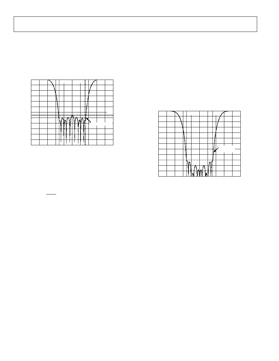
AD6654
Rev. 0 | Page 40 of 88
control register bypasses this fixed coefficient HB filter. The
filter is useful only in certain filter configurations and bypassing
it for other applications results in power savings. For example,
the filter is useful in narrow-band applications in which more
filtering is required, as compared to wide-band applications, in
which a higher output rate might prohibit the use of a decimat-
ing filter. The response of the HB2 filter is shown in Figure 52.
05156-041
FRACTION OF HB2 INPUT SAMPLE RATE
0
0.1
0.2
0.3
0.4
0.5
0.6
0.7
0.8
0.9
dBc
0.01
19.99
29.99
9.99
39.99
49.99
60.00
70.00
80.00
90.00
100.00
110.00
120.00
65
0.66
0.34
HB2 RESPONSE
Figure 52. HB2 Filter Response to the Input Rate of the Filter
The filter input sample rate is the same as the FIR2 filter output
rate and is given by one of the following equations:
f
HB2
= f
FIR2
= f
HB1
,
if HB1 is bypassed
f
HB2
= f
FIR2
=
2
HB1
f
,
if HB1 is not bypassed
where:
f
FIR2
is the input rate of the FIR2 filter.
f
HB2
is the input rate of the HB2 filter.
The input to the filter has a maximum of 75 MHz. The
maximum output rate when not bypassed is 37.5 MHz.
The filter has a ripple of 0.00075 dB and rejection of 81 dB. For
an alias rejection of 81 dB, the alias-protected bandwidth is 33%
of the filter input sample rate. The bandwidth of the filter for a
ripple of 0.00075 dB is the same as alias-protected bandwidth,
due to the nature of half-band filters. The 3 dB bandwidth of
this filter is 47% of the filter input sample rate. For example, if
the sample rate into the filter is 25 MHz, then the alias-
protected bandwidth of the HB2 filter is 8.25 MHz (33% of
25 MHz). If the bandwidth of the required carrier is greater
than 8.25 MHz, then HB2 might not be useful.
05156-042
FRACTION OF HB2 INPUT SAMPLE RATE
0
0.1
0.2
0.3
0.4
0.5
0.6
0.7
0.8
0.9
dBc
0.01
19.99
29.99
9.99
39.99
49.99
60.00
70.00
80.00
90.00
100.00
110.00
120.00
90
0.66
0.34
FIR2 + HB2
RESPONSE
Figure 53. Composite Response of FIR2 and HB2 Filters to Their Input Rates
f
HB1
is the input rate of the HB1 filter.

AD6654
Rev. 0 | Page 41 of 88
INTERMEDIATE DATA ROUTER
Following the FIR-HB cascade filters is the intermediate data
router. This data router consists of muxes that allow the I and Q
data from any channel front end (input port + NCO + CIC +
FIRHB) to be processed by any channel back end (MRCF +
DRCF + CRCF). The choice of channel front end is made by
programming a 3-bit MRCF data select word in the MRCF
control register. The valid values for this word and their
corresponding settings are listed in Table 19.
Table 19. Data Router Select Settings
MRCF Data Select[2:0]
Data Source
000 Channel
0
001 Channel
1
010 Channel
2
011 Channel
3
1x0 Channel
4
1x1 Channel
5
Allowing different channel back ends to select different channel
front ends is useful in the polyphase implementation of filters.
When multiple AD6654 channels are used to process a single
carrier, a single-channel front end feeds more than one channel
back end. After processing through the channel back ends (RCF
filters), the data is interleaved back from all the polyphased
channels.

AD6654
Rev. 0 | Page 42 of 88
MONO-RATE RAM COEFFICIENT FILTER (MRCF)
The MRCF is a programmable sum-of-products FIR filter. This
filter block comes after the first data router and before the
DRCF and CRCF programmable filters. It consists of a maxi-
mum of eight taps with 6-bit programmable coefficients. Note
that this block does not decimate and is used as a helper filter
for the DRCF and CRCF filters that follow in the signal chain.
The number of filter taps that are to be calculated is program-
mable using the 3-bit number-of-taps word in the MRCF
control register of the channel under consideration. The 3-bit
word programmed is one less than the number of filter taps.
The coefficients themselves are programmed in eight MRCF
coefficient memory registers for individual channels. The input
and output data to the block are both 20-bit.
SYMMETRY
Though the MRCF filter does not require symmetrical filters, if
the filter is symmetrical, then the symmetry bit in the MRCF
control register should be set. When this bit is set, only half of
the impulse response needs to be programmed into the MRCF
coefficient memory registers. For example, if the number of
filter taps is equal to five or six and the filter is symmetrical,
then only three coefficients need to be written into the coeffi-
cient memory. For both symmetrical and asymmetrical filters,
the number of filter taps is limited to eight.
CLOCK RATE
The MRCF filter runs on an internal high speed PLL clock. This
clock rate can be as high as 200 MHz. If the half clock rate bit in
the MRCF control register is set, then only half the PLL clock
rate is used (maximum of 100 MHz). This results in power
savings, but can only be used if certain conditions are met.
Because this filter is nondecimating, the input and output rates
are both the same and equal to one of the following:
f
MRCF
= f
HB2
,
if HB2 is not bypassed
f
MRCF
=
2
HB2
f
,
if HB2 is not bypassed
If f
PLLCLK
is the PLL clock and if
f
MRCF
× N
TAPS
<=
2
PLLCLK
f
,
then half of the PLL clock can be used for processing (power
savings). Otherwise, the PLL clock should be used.
BYPASS
The MRCF filter can be used in normal operation or bypassed
using the MRCF bypass bit in the MRCF control register. When
the filter is bypassed, the output of the filter is the same as the
input of the filter. Bypassing the MRCF filter when not required
results in power savings.
SCALING
The output of the MRCF filter can be scaled by using the 2-bit
MRCF scaling word in the MRCF control register. Table 20
shows the valid values for the 2-bit word and their
corresponding settings.
Table 20. MRCF Scaling Factor Settings
MRCF Scale Word[1:0]
Scaling Factor
00
18.06 dB attenuation
01
12.04 dB attenuation
10
6.02 dB attenuation
11
No scaling, 0 dB

AD6654
Rev. 0 | Page 43 of 88
DECIMATING RAM COEFFICIENT FILTER (DRCF)
Following the MRCF is the programmable DRCF FIR filter.
This filter can calculate up to 64 asymmetrical filter taps or up
to 128 symmetrical filter taps. The filter is also capable of a
programmable decimation rate from 1 to 16. A flexible
coefficient offset feature allows loading multiple filters into the
coefficient RAM and changing the filters on the fly. The
decimation phase feature allows a polyphase implementation,
where multiple AD6654 channels are used for processing a
single carrier.
The DRCF filter has 20-bit input and output data and 14-bit
coefficient data. The number of filter taps to calculate is
programmable and is set in the DRCF taps register. The value
of the number of taps minus one is written to this register.
For example, a value of 19 in the register corresponds to
20 filter taps.
The decimation rate is programmable using the 4-bit DRCF
decimation rate word in the DRCF control register. Again, the
value written is the decimation rate minus one.
BYPASS
The DRCF filter can be used in normal operation or bypassed
using the DRCF bypass bit in the DRCF control register. When
the DRCF filter is bypassed, no scaling is applied and the output
of the filter is the same as the input to the DRCF filter.
SCALING
The output of the DRCF filter can be scaled using the 2-bit
DRCF scaling word in the DRCF control register. Table 21 lists
the valid values for the 2-bit word and their corresponding
settings.
Table 21. DRCF Scaling Factor Settings
DRCF Scale Word[1:0]
Scaling Factor
00
18.06 dB attenuation
01
12.04 dB attenuation
10
6.02 dB attenuation
11
No scaling, 0 dB
SYMMETRY
The DRCF filter does not require symmetrical filters. However,
if the filter is symmetrical, then the symmetry bit in the DRCF
control register should be set. When this bit is set, only half of
the impulse response needs to be programmed into the DRCF
coefficient memory registers. For example, if the number of
filter taps is equal to 15 or 16 and the filter is symmetrical, then
only eight coefficients need to be written into the coefficient
memory. Because a total of 64 taps can be written into the
memory registers, the DRCF can perform 64 asymmetrical
filter taps or 128 symmetrical filter taps.
COEFFICIENT OFFSET
More than one set of filter coefficients can be loaded into
coefficient RAM at any given time (given sufficient RAM
space). The coefficient offset can be used in this case to access
the two or more different filters. By changing the coefficient
offset, the filter coefficients being accessed can be changed on
the fly. This decimal offset value is programmed in the DRCF
coefficient offset register. When this value is changed during the
calculation of a particular output data sample, the sample
calculation is completed using the old coefficients, and the new
coefficient offset from the next data sample calculation is used.
DECIMATION PHASE
When more than one channel of AD6654 is used to process one
carrier, polyphase implementation of corresponding channels'
DRCF or CRCF is possible using the decimation phase feature.
This feature can be used only under certain conditions. The
decimation phase is programmed using the 4-bit DRCF
decimation phase word of the DRCF control register.
MAXIMUM NUMBER OF TAPS CALCULATED
The output rate of the DRCF filter is given by
DRCF
MRCF
DRCF
M
f
f
=
where:
f
MRCF
is the data rate out of the MRCF filter and into the DRCF
filter.
M
DRCF
is the decimation rate in the DRCF filter.
The DRCF filter consists of two multipliers (one each for the
I and Q paths). Each multiplier, working at the high speed clock
rate (PLL clock), can do one multiply (or one tap) per high
speed clock cycle. Therefore, the maximum number of filter
taps that can be calculated (symmetrical or asymmetrical filter)
is given by
Maximum Number of Taps
= ceil
DRCF
PLLCLK
f
f
- 1
where:
f
PLLCLK
is the high speed internal processing clock generated by
the PLL clock multiplier.
f
DRCF
is the output rate of the DRCF filter, previously calculated.

AD6654
Rev. 0 | Page 44 of 88
PROGRAMMING DRCF REGISTERS FOR
AN ASYMMETRICAL FILTER
To program the DRCF registers for an asymmetrical filter:
1.
Write NTAPS 1 in the DRCF taps register, where
NTAPS is the number of filter taps. The absolute
maximum value for NTAPS is 64 in asymmetrical filter
mode.
2.
Write 0 for the DRCF coefficient offset register.
3.
Write 0 for the symmetrical filter bit in the DRCF control
register.
4.
Write the start address for the coefficient RAM, typically
equal to the coefficient offset register in the DRCF start
address register.
5.
In the DRCF stop address register, write the stop address
for the coefficient RAM, typically equal to the following:
Coefficient Offset + NTAPS - 1
6.
Write all coefficients in reverse order (start with last
coefficient) to the DRCF coefficient memory register. If in
8-bit microport mode or serial port mode, write the lower
byte of the memory register first and then the higher byte.
After each write access to the DRCF coefficient memory
register, the internal RAM address is incremented starting
with the start address and ending with the stop address.
Note that each write or read access increments the internal
RAM address. Therefore, all coefficients should be read first
before reading them back. Also, for debugging purposes, each
RAM address can be written individually by making the start
and stop addresses the same. Therefore, to program one RAM
location, the user writes the address of the RAM location to
both the start and stop address registers, and then writes the
coefficient memory register.
PROGRAMMING DRCF REGISTERS FOR A
SYMMETRIC FILTER
To program the DRCF registers for a symmetrical filter:
1.
Write NTAPS 1 in the DRCF taps register, where
NTAPS is the number of filter taps. The absolute
maximum value for NTAPS is 128 in symmetric filter
mode.
2.
Write ceil(64 NTAPS/2) for the DRCF coefficient offset
register, where the ceil function takes the closest integer
greater than or equal to the argument.
3.
Write 1 for the symmetrical filter bit in the DRCF control
register.
4.
Write the start address for the coefficient RAM, typically
equal to coefficient offset register, in the DRCF start
address register.
5.
Write the stop address for the coefficient RAM, typically
equal to ceil(NTAPS/2) 1, in the DRCF stop address
register.
6.
Write all coefficients to the DRCF coefficient memory
register, starting with the middle of the filter and working
towards the end of the filter. When coefficients are
numbered 0 to NTAPS 1, the middle coefficient is given
by the coefficient number ceil(NTAPS/2). If in 8-bit
microport mode or serial port mode, write the lower byte
of the memory register first and then the higher byte.
After each write access to the DRCF coefficient memory
register, the internal RAM address is incremented starting
with the start address and ending with the stop address.
Note that each write or read access increments the internal
RAM address. Therefore, all coefficients should be read first
before reading them back. Also, for debugging purposes, each
RAM address can be written individually by making the start
and stop addresses the same. Therefore, to program one RAM
location, the user writes the address of the RAM location to
both the start and stop address registers, and then writes the
coefficient memory register.

AD6654
Rev. 0 | Page 45 of 88
CHANNEL RAM COEFFICIENT FILTER (CRCF)
Following the DRCF is the programmable decimating CRCF
FIR filter. The only difference between the DRCF and CRCF
filters is the coefficient bit width. The DRCF has 14-bit
coefficients, while the CRCF has 20-bit coefficients.
This filter can calculate up to 64 asymmetrical filter taps or up
to 128 symmetrical filter taps. The filter is capable of a
programmable decimation rate from 1 to 16. The flexible
coefficient offset feature allows loading multiple filters into the
coefficient RAM and changing the filters on the fly. The
decimation phase feature allows for a polyphase implementa-
tion in which multiple AD6654 channels are used to process a
single carrier.
The CRCF filter has 20-bit input and output data and 20-bit
coefficient data. The number of filter taps to calculate is
programmable and is set in the CRCF taps register. The value
of the number of taps minus one is written to this register. For
example, a value of 19 in the register corresponds to 20 filter
taps. The decimation rate is programmable using the 4-bit
CRCF decimation rate word in the CRCF control register.
Again, the value written is the decimation rate minus one.
BYPASS
The CRCF filter can be used in normal operation or bypassed
using the CRCF bypass bit in the CRCF control register. When
the CRCF filter is bypassed, no scaling is applied and the output
of the filter is the same as the input to the CRCF filter.
SCALING
The output of the CRCF filter can be scaled using the 2-bit
CRCF scaling word in the CRCF control register. Table 22
shows the valid values for the 2-bit word and the corresponding
settings. |
COEFF
| is the sum of all coefficients (in normalized
form) used to calculate the FIR filter.
Table 22. CRCF Scaling Factor Settings
CRCF Scale Word[1:0]
Scaling Factor
00
18.06 dB attenuation
01
12.04 dB attenuation
10
6.02 dB attenuation
11
No scaling, 0 dB
SYMMETRY
The CRCF filter does not require symmetrical filters. However,
if the filter is symmetrical, then the symmetry bit in the CRCF
control register should be set. When this bit is set, only half the
impulse response needs to be programmed into the CRCF
coefficient memory registers. For example, if the number of
filter taps is equal to 15 or 16 and the filter is symmetric, then
only eight coefficients need to be written into the coefficient
memory.
Because a total of 64 taps can be written into the memory
registers, the CRCF can perform 64 asymmetrical filter taps or
128 symmetrical filter taps.
COEFFICIENT OFFSET
More than one set of filter coefficients can be loaded into the
coefficient RAM at any time (given sufficient RAM space). The
coefficient offset can be used in this case to access the two or
more different filters. By changing the coefficient offset, the
filter coefficients being accessed can be changed on the fly.
This decimal offset value is programmed in the CRCF
coefficient offset register. When this value is changed during
the calculation of a particular output data sample, the sample
calculation is completed using the old coefficients and the new
coefficient offset is brought into effect from the next data
sample calculation.
DECIMATION PHASE
When more than one channel of the AD6654 is used to process
one carrier, polyphase implementation of the corresponding
channels' DRCF or CRCF is possible using the decimation
phase feature. This feature can be used only under certain
conditions. The decimation phase is programmed using the
4-bit CRCF decimation phase word of the CRCF control
register.
MAXIMUM NUMBER OF TAPS CALCULATED
The output rate of the CRCF filter is given by
CRCF
DRCF
CRCF
M
f
f
=
where:
f
DRCF
is the data rate out of the DRCF filter and into the CRCF
filter.
M
CRCF
is the decimation rate in the CRCF filter.
The CRCF filter consists of two multipliers (one each for the
I and Q paths). Each multiplier, working at the high speed clock
rate (PLL clock), can multiply (or tap once). Therefore, the
maximum number of filter taps that can be calculated
(symmetrical or asymmetrical filter) is given by
Maximum Number of Taps
= ceil
CRCF
PLLCLK
f
f
- 1
f
PLLCLK
is the high speed internal processing clock generated by
the PLL clock multiplier.
f
CRCF
is the output rate of the CRCF filter as previously
calculated.

AD6654
Rev. 0 | Page 46 of 88
PROGRAMMING CRCF REGISTERS FOR AN
ASYMMETRICAL FILTER
To program the CRCF registers for an asymmetrical filter:
1.
Write NTAPS 1 in the CRCF taps register, where NTAPS
is the number of filter taps. The absolute maximum value
for NTAPS is 64 in asymmetrical filter mode.
2.
Write 0 for the CRCF coefficient offset register.
3.
Write 0 for the symmetrical filter bit in the CRCF control
register.
4.
In the CRCF start address register, write the start address
for the coefficient RAM, typically equal to the coefficient
offset register.
5.
In the CRCF stop address register, write the stop address
for the coefficient RAM, typically equal to the following:
Coefficient Offset
+ NTAPS 1
6.
Write all coefficients in reverse order (start with last
coefficient) to the CRCF coefficient memory register. In
8 bit microport mode or serial port mode, write the lower
byte of the memory register first and then the higher byte.
In 16-bit microport mode, write the lower 16-bits of the
CRCF memory register first and then the high four bits.
After each write access to the CRCF coefficient memory
register, the internal RAM address is incremented starting
with the start address and ending with the stop address.
Note that each write or read access increments the internal
RAM address. Therefore, all coefficients should be read first
before reading them back. Also, for debugging purposes, each
RAM address can be written individually by making the start
and stop addresses the same. Therefore, to program one RAM
location, the user writes the address of the RAM location to
both the start and stop address registers, and then writes the
coefficient memory register.
PROGRAMMING CRCF REGISTERS FOR A
SYMMETRICAL FILTER
To program the CRCF registers for a symmetrical filter:
1.
Write NTAPS 1 in the CRCF taps register, where NTAPS
is the number of filter taps. The absolute maximum value
for NTAPS is 128 in symmetrical filter mode.
2.
Write ceil(64 NTAPS/2) for the CRCF coefficient offset
register, where the ceil function takes the closest integer
greater than or equal to the argument.
3.
Write 1 for the symmetrical filter bit in the CRCF control
register.
4.
In the CRCF start address register, write the start address
for the coefficient RAM, typically equal to the coefficient
offset register.
5.
In the CRCF stop address register, write the stop address
for the coefficient RAM, typically equal to
ceil
(NTAPS/2) 1.
6.
Write all coefficients to the CRCF coefficient memory
register, starting with middle of the filter and working
towards the end of the filter. When coefficients are
numbered 0 to NTAPS 1, the middle coefficient is given
by the coefficient number ceil(NTAPS/2). In 8-bit
microport mode or serial port mode, write the lower byte
of the memory register first and then the higher byte. In
16-bit microport mode, write the lower 16-bits of the
CRCF memory register first and then the high four bits.
After each write access to the CRCF coefficient memory
register, the internal RAM address is incremented starting
with the start address and ending with the stop address.
Note that each write or read access increments the internal
RAM address. Therefore, all coefficients should be read first
before reading them back. Also, for debugging purposes, each
RAM address can be written individually by making the start
and stop addresses the same. Therefore, to program one RAM
location, the user writes the address of the RAM location to
both the start and stop address registers, and then writes the
coefficient memory register.
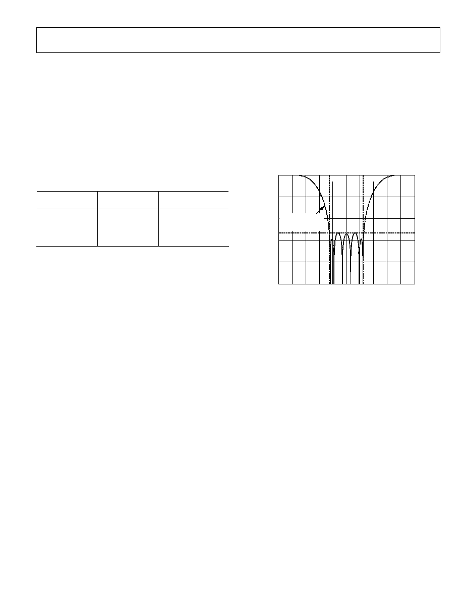
AD6654
Rev. 0 | Page 47 of 88
INTERPOLATING HALF-BAND FILTER
The AD6654 has interpolating half-band FIR filters that
immediately follow the CRCF programmable FIR filters and
precede the second data router. Each interpolating half-band
filter takes 22-bit I and 22-bit Q data from the preceding CRCF
and outputs rounded 22-bit I and 22-bit Q data to the second
data router. A 10-tap fixed coefficient filter is implemented in
this stage. The maximum input rate into this block is 17 MHz.
Consequently, the maximum output is constrained to 34 MHz.
The normalized coefficients used in the implementation and
the 10-bit decimal equivalent value of the coefficients are listed
in Table 23. Other coefficients are 0.
Table 23. Interpolating HB Filter Fixed Coefficients
Coefficient
Number
Normalized
Coefficient
Decimal Coefficient
(10-Bit)
C1, C11
0.02734375
14
C3, C9
-0.12890625
-66
C5, C7
0.603515625
309
C6
1
512
The half-band filters interpolate the incoming data by 2×. For a
channel running at 2× the chip rate, the half-band can be used
to output channel data at 4× the chip rate. The interpolation
operation creates an image of the baseband signal, which is
filtered out by the half-band filter.
The image rejection of this filter is about 55 dB, but is sufficient
because the image is from the desired signal, not an interfering
signal. Note that the interpolating half-band filter can be
enabled by writing Logic 1 to Bit 9 of the MRCF control
registers.
The frequency response of the interpolating half-band FIR is
shown in Table 23 with respect to the chip rate. The input rate
to this filter is 2× the chip rate, and the output rate is 4× the
chip rate.
05156-043
FREQUENCY AS FRACTION OF INPUT RATE
0
0.2
0.4
0.6
0.8
1.0
1.2
1.4
1.6
1.8
dBc
0
20
40
60
80
100
53
0.75
1.25
INTERPOLATING
HALF-BAND
FILTER RESPONSE
Figure 54. Interpolating Half-Band Frequency Response
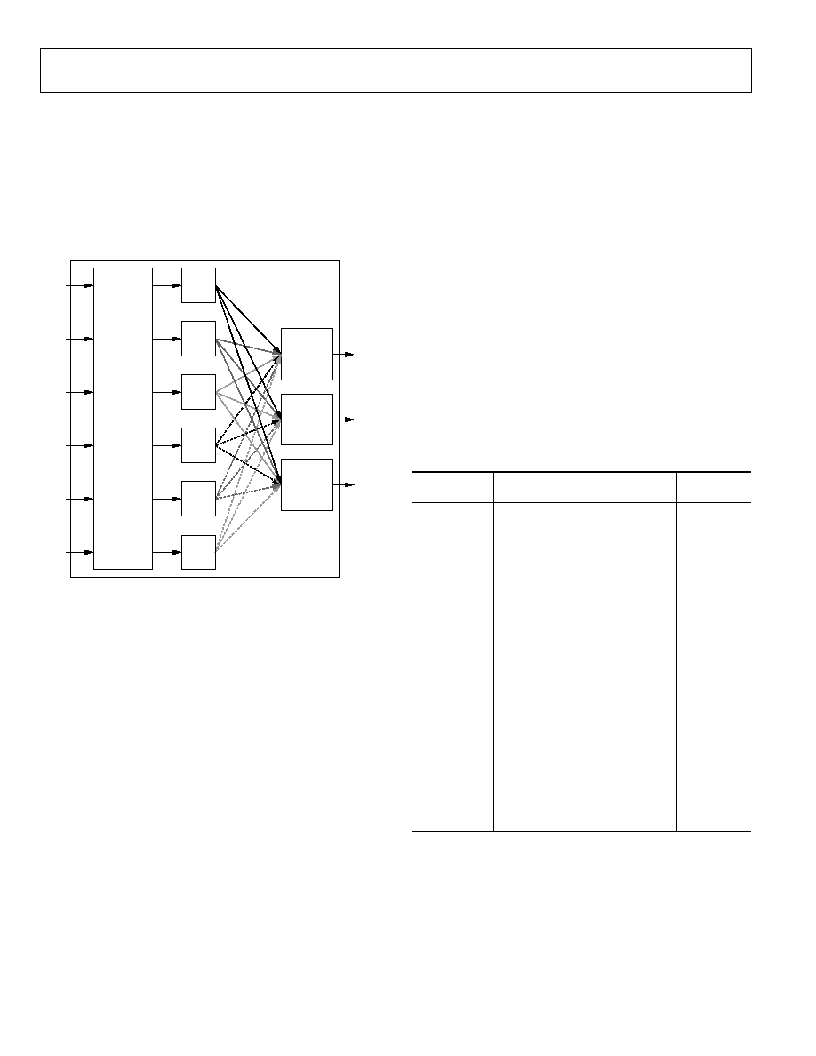
AD6654
Rev. 0 | Page 48 of 88
OUTPUT DATA ROUTER
The output data router circuit precedes the six AGCs of the
final output block and immediately follows interpolating half-
band filters. This block consists of two subblocks. The first
block is responsible for combining (interleaving) data from
more than one channel into a single stream of data. The second
block performs complex filter completion, as explained later in
this section. The combined data is passed on to the AGCs.
STREAM
CONTROL
PARALLEL
PORT A
PARALLEL
PORT C
PARALLEL
PORT B
AGC0
AGC0
CH0
AGC1
AGC1
CH1
AGC2
AGC2
CH2
AGC3
AGC3
CH3
AGC4
AGC4
CH4
AGC5
AGC5
CH5
05156-044
Figure 55. Block Diagram of the Output Data Router
INTERLEAVING DATA
In some cases, filtering using a single channel is insufficient. For
such setups, it is advantageous to combine the filtering
resources of multiple channels rather than using filtering
resources from a single channel.
Multiple channels can be set up to co-process the ADC input
port data with the same NCO and filter setups. The decimation
phase values in one of the RCF filters are set such that the
channel's filters are exactly out of phase with each other. In the
data router, these multiple channels are interleaved (combined)
to form a single stream of data. Because each individual channel
is decimated more than it would have been if a single channel
were filtering, more number-of-filter taps can be calculated.
This is best illustrated with an example:
Two channels need to work together to produce a filter at an
output rate of 9.216 MHz, when the input rate is 92.16 MHz.
Each channel is decimated by a factor of 20 (total decimation)
to achieve the desired output rate of 4.608 MHz each. This
compares to a decimation of 10, if a single channel were
working towards filtering.
The same coefficients are programmed into both of the
channels' RCF filters, and the decimation phases are set to 0
and 1. The decimation phases can be set to 0 for one channel
and 1 for the second channel in the pair. This causes the first
channel to produce the even outputs of the filter, and the
second to produce the odd outputs of the filter. The streams
are then recombined (interleaved) to produce the desired
9.216 MHz output rate. The benefit is that now each channel's
RCF has time to calculate twice as many taps, because it has a
lower output rate.
The interleaving function is a simple time-multiplexing func-
tion, with lower data rate on the input side and higher data rate
on the output side. The output data rate is the sum of all input
stream data rates that are combined.
The channels that need to be combined are programmable with
sufficient flexibility. Table 24 gives the combinations that are
possible using a 4-bit word (stream control bits) in the Parallel
Port Control 2 register.
Table 24. Stream Control Bit Combinations and Selections
Stream
Control Bits
Output Streams
Number of
Streams
0000
Ch 0, Ch 1 combined; Ch 2, Ch 3,
Ch 4, Ch 5 independent
5
0001
Ch 0, Ch 1, Ch 2 combined; Ch 3,
Ch 4, Ch 5 independent
4
0010
Ch 0, Ch 1, Ch 2, Ch 3 combined;
Ch 4, Ch 5 independent
3
0011
Ch 0, Ch 1, Ch 2, Ch 3, Ch 4
combined; Ch 5 independent
2
0100
Ch 0, Ch 1, Ch 2, Ch 3, Ch 4, Ch 5
combined
1
0101
Ch 0, Ch 1, Ch 2 combined; Ch 3,
Ch 4, Ch 5 combined
2
0110
Ch 0, Ch 1 combined; Ch 2, Ch 3
combined; Ch 4, Ch 5 combined
3
0111
Ch 0, Ch 1 combined; Ch 2, Ch 3
combined; Ch 4, Ch 5 independent
3
1000
Ch 0, Ch 1, Ch 2 combined; Ch 3,
Ch 4 combined; Ch 5 independent
3
1001
Ch 0, Ch 1, Ch 2, Ch 3 combined;
Ch 4, Ch 5 combined
2
Any other
state
Independent channels
6
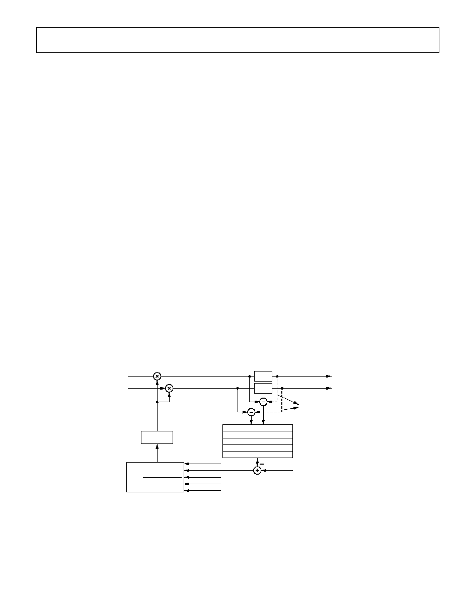
AD6654
Rev. 0 | Page 49 of 88
AUTOMATIC GAIN CONTROL
The AD6654 is equipped with six independent automatic gain
control (AGC) loops that directly follow the second data router
and immediately precede the parallel output ports. Each AGC
circuit has 96 dB of range. It is important that the decimating
filters of the AD6654 preceding the AGC reject unwanted
signals, so that each AGC loop is operating only on the carrier
of interest, and carriers at other frequencies do not affect the
ranging of the loop.
The AGC compresses the 22-bit complex output from the
second data router into a programmable word size of 4 to 8, 10,
12, or 16 bits. Because the small signals from the lower bits are
pushed in to higher bits by adding gain, the clipping of the
lower bits does not compromise the SNR of the signal of
interest.
The AGC maintains a constant mean power on the output
despite the level of the signal of interest, allowing operation in
environments where the dynamic range of the signal exceeds
the dynamic range of the output resolution. The output width of
the AGC is set by writing a 3-bit AGC word-length word in the
AGC control register of the individual channel's memory map.
The AGC can be bypassed, if needed, and, when bypassed, the
24-bit complex input word remains truncated to a 16-bit value
that is output through the parallel port output. The six AGCs
available on the AD6654 are programmable through the six
channel memory maps. AGCs corresponding to individual
channels can be bypassed by writing Logic 1 to the AGC bypass
bit in the AGC control register.
Three sources of error can be introduced by the AGC function:
underflow, overflow, and modulation. Underflow is caused by
truncation of bits below the output range. Overflow is caused by
clipping errors when the output signal exceeds the output range.
Modulation error occurs when the output gain varies while
receiving data.
The desired signal level should be set based on the probability
density function of the signal, so that the errors due to under-
flow and overflow are balanced. The gain and damping values
of the loop filter should be set, so that the AGC is fast enough to
track long-term amplitude variations of the signal that might
cause excessive underflow or overflow, but slow enough to
avoid excessive loss of amplitude information due to the
modulation of the signal.
AGC LOOP
The AGC loop is implemented using a log-linear architecture. It
contains four basic operations: power calculation, error calcula-
tion, loop filtering, and gain multiplication.
The AGC can be configured to operate in either desired signal
level mode or desired clipping level mode. The mode is set by
the AGC clipping error bit of the AGC control register. The
AGC adjusts the gain of the incoming data according to how far
it is from a given desired signal level or desired clipping level,
depending on the selected mode of operation.
Two data paths to the AGC loop are provided: one before the
clipping circuitry and one after the clipping circuitry, as shown
in Figure 56. For the desired signal level mode, only the I/Q
path prior to the clipping is used. For the desired clipping level
mode, the difference of the I/Q signals from before and after the
clipping circuitry is used.
z
P
I
Q
2×
POWER OF 2
P POLE
R DESIRED
I
Q
CLIP
22
BITS
PROGRAMMABLE
BIT WIDTH
ERROR
K1 GAIN
USED ONLY FOR
DESIRED CLIPPING
LEVEL MODE
GAIN MULTIPLIER
K2 GAIN
E ERROR
THRESHOLD
SQUARE ROOT
AVERAGE 1 16384 SAMPLES
DECIMATE 1 4096 SAMPLES
log
2
(x)
MEAN SQUARE (I
2
+ Q
2
)
CLIP
05156-045
Kz
1
1 (1 + )
1
+ Pz
2
G (z) =
Figure 56. Block Diagram of the AGC

AD6654
Rev. 0 | Page 50 of 88
DESIRED SIGNAL LEVEL MODE
In this mode of operation, the AGC strives to maintain the
output signal at a programmable set level. The desired signal
level mode is selected by writing Logic 0 into the AGC clipping
error enable bit of the AGC control register. The loop finds the
square (or power) of the incoming complex data signal by
squaring I and Q and adding them.
The AGC loop has an average and decimate block. This average
and decimate operation takes place on power samples and
before the square root operation. This block can be pro-
grammed to average from 1 to 16,384 power samples, and the
decimate section can be programmed to update the AGC once
every 1 to 4,096 samples. The limitation on the averaging
operation is that the number of averaged power samples should
be a multiple of the decimation value (1×, 2×, 3×, or 4×).
The averaging and decimation effectively means that the AGC
can operate over averaged power of 1 to 16,384 output samples.
Updating the AGC once every 1 to 4,096 samples and operating
on average power facilitates the implementation of the loop
filter with slow time constants, where the AGC error converges
slowly and makes infrequent gain adjustments. It is also useful
when the user wants to keep the gain scaling constant over a
frame of data or a stream of symbols.
Due to the limitation that the number of average samples must
be a multiple of the decimation value, only the multiple
numbers 1, 2, 3, or 4 are programmed. This is set using the
AGC average samples word in the AGC average sample register.
These averaged samples are then decimated with decimation
ratios programmable from 1 to 4,096. This decimation ratio is
defined in the 12-bit AGC update decimation register.
The average and decimate operations are tied together and
implemented using a first-order CIC filter and FIFO registers.
Gain and bit growth are associated with CIC filters and depend
on the decimation ratio. To compensate for the gain associated
with these operations, attenuation scaling is provided before the
CIC filter.
This scaling operation accounts for the division associated with
the averaging operation as well as the traditional bit growth in
CIC filters. Because this scaling is implemented as a bit-shift
operation, only coarse scaling is possible. Fine scaling is imple-
mented as an offset in the request level, as explained later in this
section. The attenuation scaling, S
CIC
, is programmable from 0
to 14 using a 4-bit CIC scale word in the AGC average samples
register and is given by
(
)
[
]
AVG
CIC
CIC
N
M
ceil
S
×
=
2
log
where:
M
CIC
is the decimation ratio (1 to 4,096).
N
AVG
is the number of averaged samples programmed as a
multiple of the decimation ratio (1, 2, 3, or 4).
For example, if a decimation ratio M
CIC
is 1,000 and N
AVG
is 3
(decimation of 1,000 and averaging of 3,000 samples), then
the actual gain due to averaging and decimation is 3,000 or
69.54 dB (log
2
(3000)). Because attenuation is implemented as a
bit-shift operation, only multiples of 6.02 dB attenuations are
possible. S
CIC
in this case is 12, corresponding to 72.24 dB. This
way, S
CIC
scaling always attenuates more than is sufficient to
compensate for the gain in the average and decimate sections
and, therefore, prevents overflows in the AGC loop. But it is
also evident that the S
CIC
scaling induces a gain error (the
difference between gain due to CIC and attenuation provided
by scaling) of up to 6.02 dB. This error should be compensated
for in the request signal level, as explained later in this section.
A logarithm to the Base 2 is applied to the output from the
average and decimate sections. These decimated power samples
are converted to rms signal samples by applying a square root
operation. This square root is implemented using a simple shift
operation in the logarithmic domain. The rms samples obtained
are subtracted from the request signal level R specified in the
AGC desired level register, leaving an error term to be
processed by the loop filter, G(z).
The user sets this programmable Request Signal Level R accord-
ing to the output signal level that is desired. The Request Signal
Level R is programmable from -0 dB to -23.99 dB in steps of
0.094 dB.
The request signal level should also compensate for errors, if
any, due to the CIC scaling, as previously explained in this
section. Therefore, the request signal level is offset by the
amount of error induced in CIC, given by
Offset
= 10 × log(M
CIC
× N
AVG
- S
CIC
× 3.01 dB
where Offset is in dB.
Continuing the previous example, this offset is given by
Offset
= 72.24 - 69.54 = 2.7 dB
So the request signal level is given by
(
)
dBFS
094
.
0
094
.
0
×
-
-
=
Offset
DSL
ceil
R
where:
R
is the request signal level.
DSL
(desired signal level) is the output signal level that the user
desires.

AD6654
Rev. 0 | Page 51 of 88
Therefore, in the previous example, if the desired signal level is
-13.8 dB, the request level R is programmed to be -16.54 dB,
compensating for the offset.
This request signal level is programmed in the 8-bit AGC
desired level register. This register has a floating-point
representation, where the 2 MSBs are exponent bits and the
6 LSBs are mantissa bits. The exponent is in steps of 6.02 dB,
and the mantissa is in steps of 0.094 dB. For example, a value
10'100101 represents 2 × 6.02 + 37 × 0.094 = 15.518 dB.
The AGC provides a programmable second-order loop filter.
The programmable parameters Gain 1 (K
1
), Gain 2 (K
2
), Error
Threshold E, and Pole P completely define the loop filter
characteristics. The error term after subtracting the request
signal level is processed by the loop filter, G(z). The open loop
poles of the second-order loop filter are 1 and P, respectively.
The loop filter parameters, Pole P and Gain K, allow the
adjustment of the filter time constant that determines the
window for calculating the peak-to-average ratio.
Depending on the value of the error term that is obtained after
subtracting the request signal level from the actual signal level,
either Gain Value K
1
or Gain Value K
2
is used. If the error is less
than the programmable threshold E, K
1
or K
2
is used. This
allows a fast loop when the error term is high (large
convergence steps required), and a slower loop function when
the error term is smaller (almost converged).
The open-loop gain used in the second-order loop G(z) is given
by one of the following equations:
K = K
1
, if Error < Error Threshold
K = K
2
, if Error > Error Threshold
The open-loop transfer function for the filter, including the gain
parameter, is
(
)
2
1
1
1
1
)
(
-
-
-
+
+
-
=
Pz
z
P
Kz
z
G
If the AGC is properly configured in terms of offset in the
request level, then there are no gains in the AGC loop except for
K, the filter gain. Under these circumstances, a closed-loop
expression for the AGC loop is given by
(
)
2
1
1
1
1
)
(
1
)
(
)
(
-
-
-
+
-
-
+
=
+
=
Pz
z
P
K
Kz
z
G
z
G
z
G
CLOSED
Program K
1
and K
2
(the gain parameters) and Pole P through
AGC loop Gain 1 and Gain 2, and AGC pole location registers
from 0 to 0.996 in steps of 0.0039 using 8-bit representation. For
example, 1000 1001 represent (137/256 = 0.535156). The error
threshold value is programmable between 0 dB and 96.3 dB in
steps of 0.024 dB. This value is programmed in the 12-bit AGC
error threshold register, using floating-point representation. It
consists of four exponent bits and eight mantissa bits. Exponent bits
are in steps of 6.02 dB and mantissa bits are in steps of 0.024 dB.
For example, 0111'10001001 represents 7 × 6.02 + 137 × 0.024 =
45.428 dB.
The user defines the open-loop Pole P and Gain K, which also
directly impact the placement of the closed-loop poles and filter
characteristics. These closed-loop poles, P
1
and P
2
, are the roots
of the denominator of the previous closed-loop transfer
function and are given by
(
) (
)
2
4
1
1
,
2
P
K
P
K
P
P
P
2
1
-
-
+
±
-
+
=
Typically, the AGC loop performance is defined in terms of its
time constant or settling time. In this case, the closed-loop poles
should be set to meet the time constants required by the AGC
loop.
The relationship between the time constant and the closed-loop
poles that can be used for this purpose is
×
=
2
1,
CIC
1,2
Rate
Sample
M
P
exp
where
1, 2
are the time constants corresponding to Pole P
1
and
Pole P
2
.
The time constants can also be derived from settling times as
given by
3
%
5
4
%
2
time
settling
or
time
settling
=
M
CIC
(CIC decimation is from 1 to 4,096), and either the settling
time or time constant are chosen by the user. The sample rate is
the sample rate of the stream coming into the AGC. If channels
were interleaved in the output data router, then the combined
sample rate into the AGC should be considered. This rate
should be used in the calculation of poles in the previous
equation, where the sample rate is mentioned.
The loop filter output corresponds to the signal gain that is
updated by the AGC. Because all computation in the loop filter
is done in logarithmic domain (to the Base 2) of the samples,
the signal gain is generated using the exponent (power of 2) of
the loop filter output.
The gain multiplier gives the product of the signal gain with
both the I and Q data entering the AGC section. This signal
gain is applied as a coarse 4-bit scaling and then as a fine scale
8-bit multiplier. Therefore, the applied signal gain is from 0 to
96.3 dB in steps of 0.024 dB. The initial signal gain is program-
mable using the AGC signal gain register. This register is again a

AD6654
Rev. 0 | Page 52 of 88
4 exponent plus 8 mantissa bit floating-point representation
similar to the error threshold. This is taken as the initial gain
value before the AGC loop starts operating.
The products of the gain multiplier are the AGC scaled outputs
with a 19-bit representation. These are, in turn, used as I and Q
for calculating the power, and the AGC error and loop are
filtered to produce the signal gain for the next set of samples.
These AGC scaled outputs can be programmed to have 4-, 5-,
6-, 7-, 8-, 10-, 12-, or 16-bit widths by using the AGC output
word-length word in the AGC control register. The AGC scaled
outputs are truncated to the required bit widths by using the
clipping circuitry, as shown in Figure 56.
Average Samples Setting
Though it is complicated to express the exact effect of the
number of averaging samples by using equations, intuitively it
has a smoothing effect on the way the AGC loop addresses a
sudden increase or a spike in the signal level. If averaging of
four samples is used, the AGC addresses a sudden increase in
signal level more slowly compared to no averaging. The same
applies to the manner in which the AGC addresses a sudden
decrease in the signal level.
DESIRED CLIPPING LEVEL MODE
Each AGC can be configured so that the loop locks onto a
desired clipping level or a desired signal level. Desired clipping
level mode is selected by writing Logic 1 in the AGC clipping
error mode bit in the AGC control register. For signals that tend
to exceed the bounds of the peak-to-average ratio, the desired
clipping level option provides a way to prevent truncating those
signals and still provide an AGC that attacks quickly and settles
to the desired output level. The signal path for this mode of
operation is shown with dotted lines in Figure 56; the operation
is similar to the desired signal level mode.
First, the data from the gain multiplier is truncated to a lower
resolution (4, 5, 6, 7, 8, 10, 12, or 16 bits) as set by the AGC
output word-length word in the AGC control register. An error
term (for both I and Q) is generated that is the difference
between the signals before and after truncation. This term is
passed to the complex squared magnitude block, for averaging
and decimating the update samples and taking their square root
to find rms samples as in desired signal level mode. In place of
the request desired signal level, a desired clipping level is
subtracted, leaving an error term to be processed by the second-
order loop filter.
The rest of the loop operates the same way as the desired signal
level mode. This way, the truncation error is calculated and the
AGC loop operates to maintain a constant truncation error
level. The only register setting that is different from the desired
signal level mode settings is that the desired clipping level is
stored in the AGC desired level registers instead of in the
request signal level.
AGC SYNCHRONIZATION
When the AGC output is connected to a RAKE receiver, the
RAKE receiver can synchronize the average and update section
to update the average power for AGC error calculation and loop
filtering. This external sync signal synchronizes the AGC
changes to the RAKE receiver and makes sure that the AGC
gain word does not change over a symbol period, which,
therefore, provides a more accurate estimation. This synchroni-
zation is accomplished by setting the appropriate bits of the
AGC control register.
Sync Select Alternatives
The AGC can receive a sync as follows:
· Channel sync: The sync signal is used to synchronize the
NCO of the channel under consideration.
· Pin sync: Selects one of the four SYNC pins.
· Sync now bit: Through the AGC control register.
When the channel sync select bit of the AGC control register is
Logic 1, the AGC receives the sync signal used by the NCO of
the corresponding channel for the start. When this bit is Logic 0,
the pin sync defined by the 2-bit SYNC pin select word in the
AGC control register provides the sync to the AGC. Apart from
these two methods, the AGC control register also has a sync
now bit that can be used to provide a sync to the AGC by
writing to this register through the microport or serial port.
SYNC PROCESS
Regardless of how a sync signal is received, the syncing process
is the same. When a sync is received, a start hold-off counter is
loaded with the 16-bit value in the AGC hold-off register, which
initiates the countdown. The countdown is based on the ADC
input clock. When the count reaches 1, a sync is initiated. When
a sync is initiated, the CIC decimation filter dumps the current
value to the square root, error estimation, and loop filter blocks.
After dumping the current value, it starts working toward the
next update value. Additionally on a sync, AGC can be initial-
ized, if the initialize AGC on sync bit is set in the AGC control
register. During initialization, the CIC accumulator is cleared
and new values for CIC decimation, number of averaging
samples, CIC scale, signal gain, open-loop Gain K
1
and Gain K
2
,
and the Pole P parameter are loaded from their respective
registers. When the initialize on sync bit is cleared, these
parameters are not loaded from the registers.
This sync process is also initiated when a channel comes out of
sleep by using the start sync to the NCO. An additional feature
is the first sync only bit in the AGC control register. When this
bit is set, only the first sync initiates the process and the remain-
ing sync signals are ignored. This is useful when syncing using a
pin sync. A sync is required only on the first pulse on this pin.
These additional features make AGC synchronization more
flexible and applicable to varied circumstances
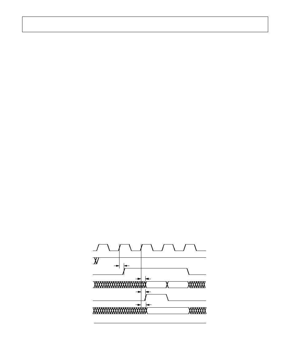
AD6654
Rev. 0 | Page 53 of 88
PARALLEL PORT OUTPUT
The AD6654 incorporates three independent 16-bit parallel
ports for output data transfer. The three parallel output ports
share a common clock, PCLK. Each port consists of a 16-bit
data bus, request signal, acknowledge signal, three channel
indicator pins, one I/Q indicator pin, one gain word indicator
pin, and a common shared PCLK pin. The parallel ports can be
configured to function in master mode or slave mode. By
default, the parallel ports are in slave mode on power-up.
Each parallel port can output data from any or all of the AGCs,
using the 1-bit enable bit for each AGC in the parallel port
control register. Even when the AGC is not required for a
certain channel, the AGC can be bypassed, but the data is still
received from the bypassed AGC. The parallel port
functionality is programmable through the two parallel port
control registers.
Each parallel port can be programmed individually to operate
in either interleaved I/Q mode or parallel I/Q mode. The mode
is selected using a 1-bit data format bit in the parallel port
control register. In both modes, the AGC gain word output can
be enabled using a 1-bit append gain bit in the parallel port
control register for individual output ports. There are six enable
bits per output port, one for each AGC in the corresponding
parallel port.
INTERLEAVED I/Q MODE
Parallel port channel mode is selected by writing a 0 to the data
format bit for the parallel port in consideration. In this mode,
I and Q words from the AGC are output on the same 16-bit data
bus on a time-multiplexed basis. The 16-bit I word is output
followed by the 16-bit Q word. The specific AGCs output by the
port are selected by setting individual bits for each of the AGCs
in the parallel port control register. Figure 57 shows the timing
diagram for the interleaved I/Q mode.
When an output data sample is available for output from an
AGC, the parallel port initiates the transfer by pulling the
PxREQ signal high. In response, the processor receiving the
data needs to pull the PxACK signal high, acknowledging that it
is ready to receive the signal. In Figure 57, PxACK is already
pulled high and, therefore, the 16-bit I data is output on the
data bus on the next PCLK rising edge after PxREQ is driven
logic high. The PxIQ signal also goes high to indicate that I data
is available on the data bus. The next PCLK cycle brings the
Q data onto the data bus. In this cycle, the PxIQ signal is driven
low. When I data and Q data are output, the channel indicator
pins PxCH[2:0] indicate the data source (AGC number).
Figure 57 is the timing diagram for interleaved I/Q mode with
the AGC gain word disabled. Figure 58 is a similar timing
diagram with the AGC gain word. In the PCLK cycle after the Q
data, the AGC gain word is output on the data bus and the
PxGAIN signal is pulled high to indicate that the gain word is
available on the parallel port. Therefore, a minimum of three or
four PCLK cycles are required to output one sample of output
data on the parallel port without or with the AGC gain word,
respectively.
PARALLEL I/Q MODE
In this mode, eight bits of I data and eight bits of Q data are
simultaneously output on the data bus during one PCLK cycle.
The I byte is the most significant byte of the port, while the
Q byte is the least significant byte. The PAIQ and PBIQ output
indicator pins are set high during the PCLK cycle. Note that if
data from multiple AGCs are output consecutively, the PAIQ
and PBIQ output indicator pins remain high until data from all
channels is output. The PACH[2:0] and PBCH[2:0] pins provide
a 3-bit binary value indicating the source (AGC number) of the
data currently being output. Figure 59 is the timing diagram for
parallel I/Q mode.
PCLK
t
DPREQ
PxREQ
PxACK
t
DPP
Px [15:0]
I [15:0]
Q [15:0]
PxIQ
t
DPIC
PxCH [2:0]
PxCH [2:0] = CHANNEL NO.
t
DPCH
PxGAIN
LOGIC LOW `0'
05156-046
Figure 57. Interleaved I/Q Mode Without an AGC Gain Word
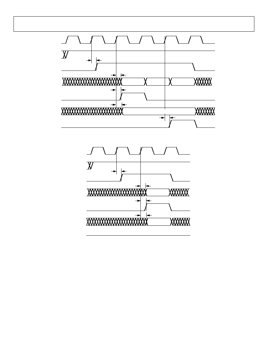
AD6654
Rev. 0 | Page 54 of 88
PCLK
t
DPREQ
PxREQ
PxACK
t
DPP
Px [15:0]
I[15:0]
Q[15:0]
PxIQ
t
DPIQ
PxCH [2:0]
PxCH [2:0] = CHANNEL #
t
DPCH
0000 +
GAIN [11:0]
PxGAIN
t
DPGAIN
05156-047
Figure 58. Interleaved I/Q Mode with an AGC Gain Word
PxCH [2:0]
PCLK
t
DPREQ
PxREQ
PxACK
t
DPP
Px [15:0]
I [15:8]
Q [15:8]
PxIQ
t
DPIQ
PxCH [2:0] =
AGC NO.
t
DPCH
PxGAIN
LOGIC LOW 0
05156-048
Figure 59. Parallel I/Q Mode Without an AGC Gain Word
When an output data sample is available for output from an
AGC, the parallel port initiates the transfer by pulling the
PxREQ signal high. In response, the processor receiving the
data needs to pull the PxACK signal high, acknowledging that it
is ready to receive the signal. In Figure 59, the PxACK is already
pulled high and, therefore, the 8-bit I data and 8-bit Q data are
simultaneously output on the data bus on the next PCLK rising
edge after PxREQ is driven logic high. The PxIQ signal also
goes high to indicate that I/Q data is available on the data bus.
When I/Q data is being output, the channel indicator pins
PxCH[2:0] indicate the data source (AGC number).
Figure 59 is the timing diagram for parallel I/Q mode with the
AGC gain word disabled. Figure 60 is a similar timing diagram
with the AGC gain word enabled. In the PCLK cycle after the
I/Q data, the AGC gain word is output on the data bus, and the
PxGAIN signal is pulled high to indicate that the gain word is
available on the parallel port. During this PCLK cycle, the PxIQ
signal is pulled low to indicate that I/Q data is not available on
the data bus. Therefore, in parallel I/Q mode, a minimum of
two PCLK cycles is required to output one sample of output
data on the parallel port without and with the AGC gain word,
respectively.
The order of data output is dependent on when data arrives at
the port, which is a function of total decimation rate, DRCF/
CRCF decimation phase, and start hold-off values. Priority
order from highest to lowest is, AGC0, AGC1, AGC2, AGC3,
AGC4, and AGC5 for both parallel I/Q and interleaved modes
of output.
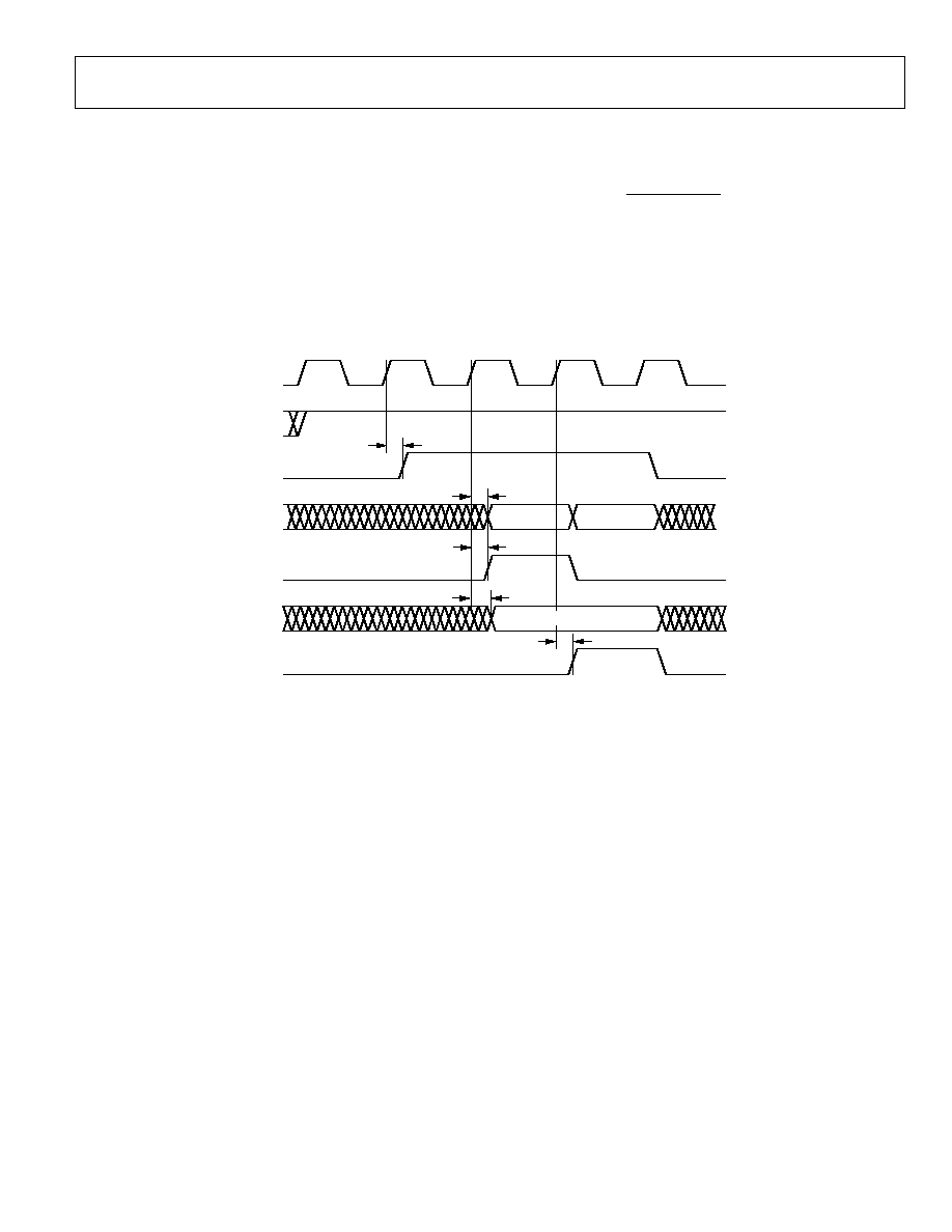
AD6654
Rev. 0 | Page 55 of 88
MASTER/SLAVE PCLK MODES
The parallel ports can operate in either master or slave mode.
The mode is set via PCLK master mode bit in the Parallel Port
Control 2 register. The parallel ports power up in slave mode to
avoid possible contentions on the PCLK pin.
In master mode, PCLK is an output derived by dividing
PLL_CLK down by the PCLK divisor. The PCLK divisor can
have a value of 1, 2, 4, or 8, depending on the 2-bit PCLK
divisor word setting in the Parallel Port Control 2 register. The
highest PLCK rate in master mode is 200 MHz. Master mode is
selected by setting the PCLK master mode bit in the Parallel
Port Control 2 register.
divisor
PCLK
rate
CLK
PLL
rate
PCLK
_
=
In slave mode, external circuitry provides the PCLK signal.
Slave mode PCLK signals can be either synchronous or
asynchronous. The maximum slave mode PCLK frequency is
also 200 MHz.
PCLK
t
DPREQ
PxREQ
PxACK
t
DPP
Px [15:0]
I [15:8]
Q [15:8]
PxIQ
t
DPIQ
PxCH [2:0]
PxCH [2:0] = CHANNEL #
t
DPCH
0000 +
GAIN [11:0]
PxGAIN
t
DPGAIN
05156-049
Figure 60. Parallel I/Q Mode with an AGC Gain Word

AD6654
Rev. 0 | Page 56 of 88
PARALLEL PORT PIN FUNCTIONS
Table 25 describes the functions of the pins used by the parallel ports.
Table 25. Parallel Port Pin Functions
Pin Name
I/O Function
PCLK I/O
Parallel Clock. PCLK can operate as a master or as a slave. This setting is dependent on the 1-bit PCLK master
mode bit in the Parallel Port Control 2 register. As an output (master mode), the maximum frequency is
CLK/N, where CLK is the AD6654 clock and N is an integer divisor of 1, 2, 4, or 8. As an input (slave mode), it
can be asynchronous or synchronous relative to the AD6654 CLK. This pin powers up as an input to avoid
possible contentions. Parallel port output pins change on the rising edge of PCLK.
PAREQ, PBREQ,
PCREQ
O
Active High Output. Synchronous to PCLK. A logic high on this pin indicates that data is available to be
shifted out of the port. When an acknowledge signal is received, data starts shifting out and this pin remains
high until all pending data has been shifted out.
PAACK, PBACK,
PCACK
I
Active High Asynchronous Input. Applying a logic low on this pin inhibits parallel port data shifting. Applying
a logic high to this pin when REQ is high causes the parallel port to shift out data according to the
programmed data mode. ACK is sampled on the rising edge of PCLK. Assuming that REQ is asserted, the
latency from the assertion of ACK to data appearing at the parallel port output is no more than 1.5 PCLK
cycles. ACK can be continuously held high; in this case, when data becomes available, shifting begins 1 PCLK
cycle after the assertion of REQ (see Figure 57, Figure 58, Figure 59, and Figure 60).
PAIQ, PBIQ, PCIQ
Parallel Output Gain Data Indicators High whenever I data is present on the parallel port data bus; otherwise
low. In parallel I/Q mode, both I data and Q data are available at the same time and, therefore, the PxIQ signal
is pulled high.
PAGAIN, PBGAIN,
PCGAIN
Parallel Output Gain Word Indicators. High whenever the AGC gain word is present on the parallel port data
bus; otherwise low.
PACH[2:0], PBCH[2:0],
PCCH[2:0]
Channel Indicator Output Ports. These pins identify data in both of the parallel port modes. The 3-bit value
identifies the source of the data (AGC number) on the parallel port when it is being shifted out.
PADATA[15:0],
PBDATA[15:0],
PCDATA[15:0]
Parallel Output Port Data Bus. Output format is twos complement. In parallel I/Q mode, 8-bit data is present;
in interleaved I/Q mode, 16-bit data is available.

AD6654
Rev. 0 | Page 57 of 88
USER-CONFIGURABLE BUILT-IN SELF-TEST (BIST)
Each channel of AD6654 includes a BIST block. The BIST,
along with an internal test signal (pseudo random test input
signal), can be used to generate a signature. This signature can
be compared with a known good device and an untested device
to see if the untested device is functional.
BIST timer bits in the BIST control register can be programmed
with a timer value that determines the number of clock cycles
that the output of the channels (output of AGC) have
accumulated. When the disable signature generation bit is
written with Logic 0, the BIST timer is counted down and a
signature register is written with the accumulated output of the
AD6654 channel.
When the BIST timer expires, the signature register for I and Q
paths can be read back to compare it with the signature register
from a known good device.

AD6654
Rev. 0 | Page 58 of 88
CHIP SYNCHRONIZATION
The AD6654 offers two types of synchronization: start sync and
hop sync. Start sync is used to bring individual channels out of
sleep after programming. It can also be used while AD6654 is
operational to resynchronize the internal clocks. Hop sync is
used to change or update the NCO frequency tuning word and
the NCO phase offset word.
Two methods can be used to initiate a start sync or hop sync:
· Soft sync is provided by the memory map registers and is
applied to channels directly through the microport or serial
port interface.
· Pin sync is provided using four hard-wired SYNC[3:0] pins.
Each channel is programmed to listen to one of these SYNC
pins and do a start sync or a hop sync when a signal is
received on these pins.
The pin synchronization configuration register (Address 0x04)
is used to make pin synchronization even more flexible. The
part can be programmed to be edge-sensitive or level-sensitive
for SYNC pins. In edge-sensitive mode, a rising edge on the
SYNC pins is recognized as a synchronization event.
START
Start refers to the startup of an individual channel or chip, or of
multiple chips. If a channel is not used, it should be put into
sleep mode to reduce power dissipation. Following a hard reset
(low pulse on the RESET pin), all channels are placed into sleep
mode. Alternatively, channels can be manually put to sleep by
writing 0 to the sleep register.
Start with Soft Sync
The AD6654 can synchronize channels or chips under micro-
processor control. The start hold-off counter, in conjunction
with the soft start enable bit and the channel enable bits, enables
this synchronization.
To synchronize the start of multiple channels via micro-
processor control:
1.
Write the channel enable register to enable one or more
channels, if the channels are inactive.
2.
Write the NCO start hold-off counter registers with the
appropriate value (greater than 0 and less than 2
16
).
3.
Write the soft sync channel enable bit(s) and soft start
synchronization enable bit high in the soft synchroniza-
tion configuration register. This starts the countdown by
the start hold-off counter. When the count reaches 1, the
channels are activated or resynchronized.
Note: When using SPI or SPORT for programming these
registers, the last step in the above procedure needs to be
repeated, that is, the soft synchronization register needs to be
written twice.
Start with Pin Sync
Four sync pins (SYNC0, SYNC1, SYNC2, and SYNC3) provide
very accurate synchronization among channels. Each channel
can be programmed to monitor any of the four sync pins.
To start the channels with a pin sync:
1.
Write the channel register to enable one more channels, if
the channels are inactive.
2.
Write the NCO start hold-off counter registers with the
appropriate value (greater than 0 and less than 2
16
).
3.
Program the channel NCO control registers to monitor
the appropriate SYNC pins.
4.
Write the start synchronization enable bit and SYNC pin
enable bits high in the pin synchronization configuration
register. This starts the countdown of the start hold-off
counter. When the count reaches 1, the channels are
activated or resynchronized.
HOP
Hop is a jump from one NCO frequency and/or phase offset to
a new NCO frequency and/or phase offset. This change in
frequency and/or phase offset can be synchronized via micro-
processor control (soft sync) or via an external sync signal
(pin sync).
Hop with Soft Sync
The AD6654 can synchronize a change in NCO frequency
and/or phase offset of multiple channels or chips under
microprocessor control. The NCO hop hold-off counter, in
conjunction with the soft hop enable bit and the channel enable
bits, enables this synchronization.
To synchronize the hop of multiple channels via microprocessor
control:
1.
Write the NCO frequency register(s) or phase offset
register(s) to the new value.
2.
Write the NCO frequency hold-off counter registers with
the appropriate value (greater than 0 and less than 2
16
).
3.
Write 0x00 to the soft synchronization configuration
register.
4.
Write the soft hop synchronization enable bit and the
corresponding soft sync channel enable bits high in the
soft synchronization configuration register. This starts the
countdown by the frequency hold-off counter. When the

AD6654
Rev. 0 | Page 59 of 88
count reaches 1, the new frequency and/or phase offset is
loaded into the NCO.
Note: When using SPI or SPORT for programming these
registers, the last step in the above procedure needs to be
repeated, that is, the soft synchronization register needs to be
written twice.
Hop with Pin Sync
Four sync pins (SYNC0, SYNC1, SYNC2, and SYNC3) provide
very accurate synchronization among channels. Each channel
can be programmed to look at any of the four sync pins.
To control the hop of channel NCO frequencies:
1.
Write the NCO frequency register(s) or phase offset
register(s) to the new value.
2.
Write the NCO frequency hold-off counter(s) to the
appropriate value (greater than 0 and less than 2
16
).
3.
Program the channel NCO control registers to monitor
the appropriate SYNC pins.
4.
Write the hop synchronization enable bit and SYNC pin
enable bits high in the pin synchronization configuration
register. This enables the countdown of the frequency
hold-off counter. When the count reaches 1, the new
frequency and/or phase offset is loaded into the NCO.

AD6654
Rev. 0 | Page 60 of 88
SERIAL PORT CONTROL
The AD6654 serial port allows all memory to be accessed
(programmed or readback) serially in one-byte words. Either
serial port or microport can be used (but not both) at any given
time. Serial port control is selected using the SMODE pin (0 =
microport, 1 = serial port). Two serial port modes are available.
An SPI-compatible port is provided as well as a SPORT. The
choice of SPI or SPORT mode is selected using the MODE pin
(0 = SPI, 1 = SPORT).
Each individual byte of serial data (address, instruction and
data) may be shifted in either MSB first or LSB first using the
MSBFIRST pin (1 = MSB first, 0 = LSB first). The serial chip
select (SCS) pin is brought low to access the device for serial
control. When the SCS pin is held high, serial programming is
inhibited.
HARDWARE INTERFACE
The pins described in Table 26 comprise the physical interface
between the user's programming device and the serial port of
the AD6654. All serial pins are inputs except for SDO, which is
an open-drain output and should be pulled high by an external
pull-up resistor (suggested value 1 k).
A complete read or write cycle requires a minimum of three
bytes to transfer, consisting of address word, instruction word,
and data-word(s). As many as 127 data-words can be
transferred during a block transfer cycle. All address,
instruction, and data-word(s) must be formatted LSB first or
MSB first to match the state of the MSBFIRST pin.
The first word for serial transfer is the internal register address.
In LSB first mode, the address is the lower-most address for the
block transfer (subsequent addresses are generated by internal
increment). In MSB first, the address is highest address for the
block transfer (subsequent addresses are generated by internal
decrement).
The second word of serial transfer contains a one-bit read/write
indicator (1 = read, 0 = write), and seven bits to define the
number of data bytes to be transferred (N). For a single data
byte transfer (N = 1); one byte is shifted into SDI for a write
transfer, or shifted out of SDO for a read transfer, and the cycle
is complete. For a block transfer, N write/read operations are
performed, and the internal register address increments
(MSBFIRST = 0) or decrements (MSBFIRST = 1) after each
data byte is clocked into SDI for a write operation, or after each
data byte is clocked out of SDO for a read operation.
Figure 61 to Figure 64 illustrate a three byte block transfer
through the serial port. Read and write operations with
MSBFIRST high and low are shown. Please note that the figures
show the sequence for write/read transfer, and actual data
should be shifted in or out based upon the status of the
MSBFIRST pin. The operation details are common to both SPI
and SPORT modes except for the use of framing signals and
timing. Individual mode details follow. In single byte transfer
mode, the count in the second byte would be reduced to one,
and the number of data bytes would be reduced to one.
Table 26. Serial Port Pins
Pin Function
SCLK
Serial Clock in Both SPI and SPORT Modes. Should have a rise/fall time of 3 ns max.
MSBFIRST
Indicates whether the first bit shifted in or out of the serial port is the MSB (1) or LSB (0) for both instruction and data-
words. Also indicates if the first instruction word (address) is a block start or a block end for multiple byte transfers. This
pin also controls the functionality when programming indirectly addressed registers.
STFS
Serial Transmit Frame Sync in SPORT Mode. STFS is not used in SPI mode.
SRFS
Serial Receive Frame Sync in SPORT Mode. SRFS is not used in SPI mode.
SDI
Serial Data Input in Both Modes. Serial data is clocked in on the rising edge of SCLK.
SDO
Serial Data Output in Both Modes. Serial data is clocked out on the rising edge of SCLK.
SCS
Active-Low Serial Chip Select in Both Modes.
SMODE
Serial Mode. Part is programmed through the serial port when this pin is high.
MODE
Mode Pin. Selects between SPI (0) and SPORT (1) modes.
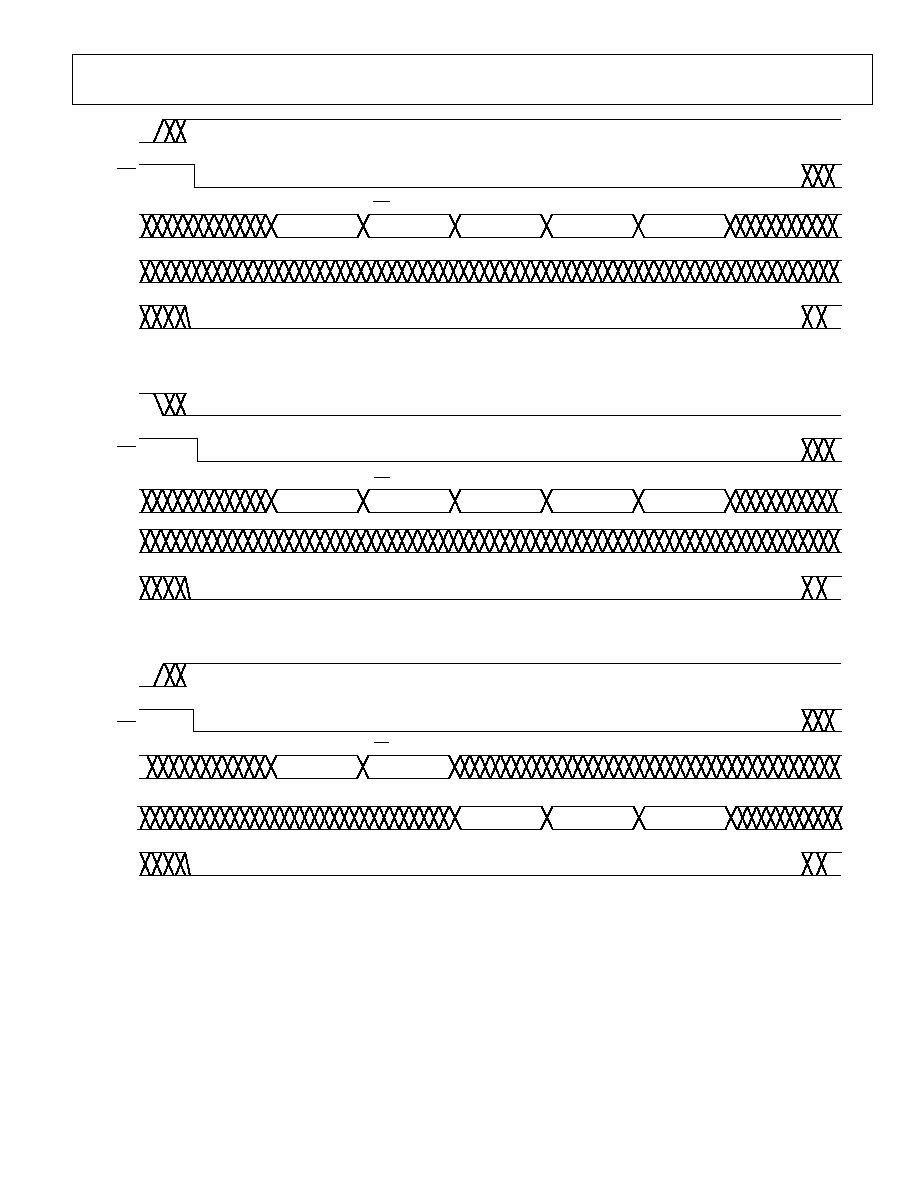
AD6654
Rev. 0 | Page 61 of 88
05156-075
MSBFIRST
SCS
SDI
SDO
MODE
0xaa
0x03
aa
aa 1
aa 2
BLOCK END ADDRESS WR + COUNT (3)
DATA TO BLOCK END
ADDRESS
DATA TO BLOCK END
ADDRESS 1
DATA TO BLOCK END
ADDRESS 2
Figure 61. Serial Write of Three Bytes with MSBFIRST = 1 (All Words are Written MSB first)
05156-076
MSBFIRST
SCS
SDO
MODE
SDI
0xaa
0x03
aa
aa + 1
aa + 2
BLOCK START
ADDRESS
WR + COUNT (3)
DATA TO BLOCK START
ADDRESS
DATA TO BLOCK START
ADDRESS + 1
DATA TO BLOCK START
ADDRESS + 2
Figure 62. Serial Write of Three Bytes with MSBFIRST = 0 (All Words are Written LSB First)
05156-077
MSBFIRST
SCS
SDO
MODE
SDI
0xaa
0x83
BLOCK END
ADDRESS
RD + COUNT (3)
aa
aa 1
DATA FROM BLOCK END
ADDRESS
DATA FROM BLOCK END
ADDRESS 1
DATA FROM BLOCK END
ADDRESS 2
aa 2
Figure 63. Serial Read of Three Bytes with MSBFIRST = 1 (All Words are Written or Read MSB First)
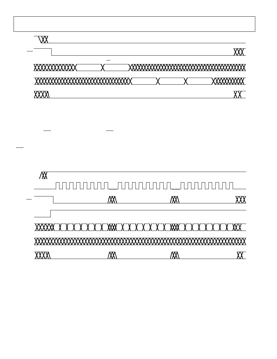
AD6654
Rev. 0 | Page 62 of 88
05156-078
MSBFIRST
SCS
MODE
SDI
SDO
0xaa
0x83
BLOCK START
ADDRESS
RD + COUNT (3)
aa
aa + 1
DATA FROM BLOCK START
ADDRESS
DATA FROM BLOCK START
ADDRESS + 1
DATA FROM BLOCK START
ADDRESS + 2
aa + 2
Figure 64. Serial Read of Three Bytes with MSBFIRST = 0 (All Words are Written or Read LSB First)
SPI MODE TIMING
In SPI mode, the SCLK should run only when data is being
transferred and SCS is logic low. If SCLK runs when SCS is logic
high, the internal shift register continues to run and instruction
words or data are lost. No external framing is necessary. The
SCS pin can be pulled low once for each byte of transfer, or kept
low for the whole length of the transfer.
SPI Write
Data on the SDI pin is registered on the rising edge of SCLK.
During a write, the serial port accumulates eight input bits
of data before transferring one byte to the internal registers.
Figure 65 and Figure 66 show one byte block transfer for
writing in MSBFIRST and LSBFIRST modes.
05156-079
MSBFIRST
SCLK
SDI
SDO
MODE
SCS
SMODE
A7
A6
A5
A4
A3
BLOCK END ADDRESS
BLOCK COUNT (Nx)
WRITE
A2
A1
A0
0
N6
N5
N4
N3
N2
N1
N0
D7
D6
D5
D4
D3
D2
D1
D0
Figure 65. SPI Write MSBFIRST = 1
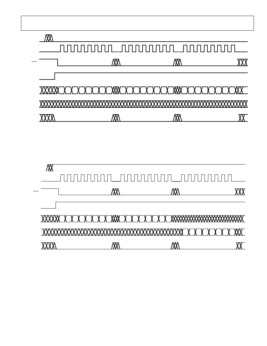
AD6654
Rev. 0 | Page 63 of 88
05156-058
MSBFIRST
SCLK
SDI
SDO
MODE
SCS
SMODE
A0
A1
A2
A3
A4
BLOCK END ADDRESS
BLOCK COUNT (Nx)
WRITE
A5
A6
A7
N0
N1
N2
N3
N4
N5
N6
0
D0
D1
D2
D3
D4
D5
D6
D7
Figure 66. SPI Write MSBFIRST = 0
SPI Read
During a typical read operation, a one byte address and one
byte instruction are written to the serial port to instruct the
internal control logic as to which registers are to be accessed.
Register readback data shifts out on the rising edge of SCLK.
The SDO pin is in a high impedance state at all times except
during a read cycle.
MSBFIRST
SCLK
SDI
SDO
MODE
SCS
SMODE
BLOCK END ADDRESS
BLOCK COUNT (Nx)
READ
A7
A6
A5
A4
A3
A2
A1
A0
1
N6
N5
N4
N3
N2
N1
N0
D7
D6
D5
D4
D3
D2
D1
D0
05156-080
Figure 67. SPI Read MSBFIRST = 1
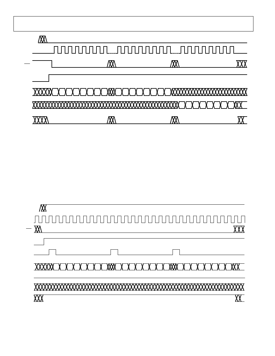
AD6654
Rev. 0 | Page 64 of 88
05156-059
MSBFIRST
SCLK
SDO
MODE
SCS
SMODE
SDI
A0
A1
A2
A3
A4
BLOCK START ADDRESS
BLOCK COUNT (Nx)
READ
A5
A6
A7
N0
N1
N2
N3
N4
N5
N6
1
D0
D1
D2
D3
D4
D5
D6
D7
Figure 68. SPI Read MSBFIRST = 0
SPORT MODE TIMING
In SPORT mode, the SCLK continuously runs, and the external
SRFS and STFS signals are used to frame the data. Incoming
framing signals SRFS (receive) and STFS (transmit) are sampled
on the falling edges of SCLK. All input and output data must be
transmitted or received in 8-bit segments starting with the
rising edge after SRFS or STFS is sampled.
SPORT Write
Serial data is sampled on the rising edge of SCLK. The data
should be MSB or LSB first, depending on the polarity of the
MSBFIRST pin. The serial port begins to sample data on the
rising edge of SCLK after SRFS is detected on the falling edge of
SCLK. Once all 8-bits of one byte are shifted in, the data is
transferred to the internal bus.
05156-081
MSBFIRST
SCLK
SDI
STFS
SDO
MODE
SCS
SMODE
SRFS
A7
A6
A5
A4
A3
BLOCK START ADDRESS
BLOCK COUNT (Nx)
WRITE
A2
A1
A0
0
N6
N5
N4
N3
N2
N1
N0
D7
D6
D5
D4
D3
D2
D1
D0
Figure 69. SPORT Write MSBFIRST = 1
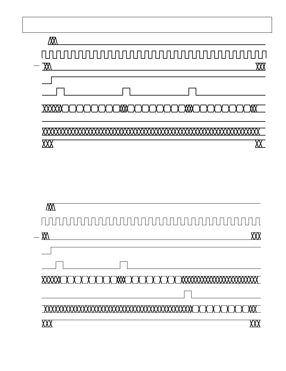
AD6654
Rev. 0 | Page 65 of 88
05156-060
MSBFIRST
SCLK
SDI
SRFS
STFS
MODE
SDO
SCS
SMODE
BLOCK START ADDRESS
BLOCK COUNT (Nx)
WRITE
A0
A1
A2
A3
A4
A5
A6
A7
N0
N1
N2
N3
N4
N5
N6
0
D0
D1
D2
D3
D4
D5
D6
D7
Figure 70. SPORT Write MSBFIRST = 0
SPORT Read
For a typical SPORT read operation, the user must write an
address byte and instruction byte to the serial port to instruct
the internal control logic as to which registers are to be
readback. STFS must be asserted for every 8-bit readback and is
sampled on the falling edge of SCLK. Data is shifted out on the
rising edge of SCLK. The SDO pin is in a high impedance state
at all times except during a read operation.
MSBFIRST
SCLK
SRFS
SDI
STFS
MODE
SDO
SCS
SMODE
05156-082
BLOCK START ADDRESS
BLOCK COUNT (Nx)
READ
A7
A6
A5
A4
A3
A2
A1
A0
1
N6
N5
N4
N3
N2
N1
N0
D7
D6
D5
D4
D3
D2
D1
D0
Figure 71. SPORT Read MSBFIRST = 1
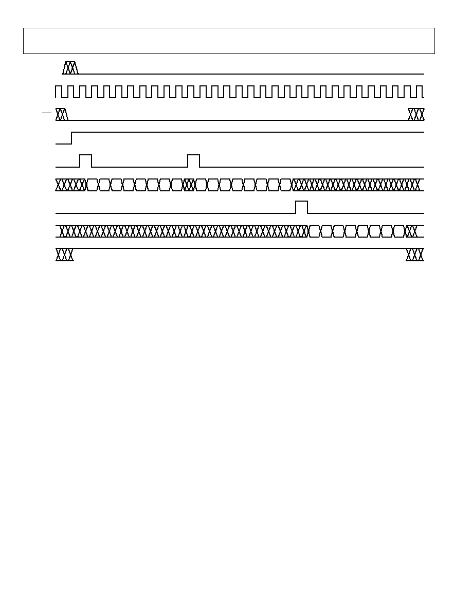
AD6654
Rev. 0 | Page 66 of 88
MSBFIRST
SCLK
SRFS
SDI
STFS
MODE
SDO
SCS
SMODE
05156-061
BLOCK START ADDRESS
BLOCK COUNT (Nx)
READ
A0
A1
A2
A3
A4
A5
A6
A7
N0
N1
N2
N3
N4
N5
N6
1
D0
D1
D2
D3
D4
D5
D6
D7
Figure 72. SPORT Read MSBFIRST = 0

AD6654
Rev. 0 | Page 67 of 88
PROGRAMMING INDIRECT ADDRESSED REGISTERS
USING SERIAL PORT
This section gives examples for programming CRCF coefficient
RAM (with an indirect addressing scheme) using the serial port
(either SPI or SPORT modes). Though the following specific
examples are for CRCF coefficient RAM programming, they can
be extended to other indirect addressed registers like DRCF
coefficient RAM. There are four possible programming scenarios,
and examples are given for all scenarios using two commands:
SerialWrite(data) and SerialRead. These commands signify an 8-
bit write to, or an 8-bit read from, the serial port (SPI or SPORT).
SerialWrite(8-bit number):
is an 8-bit write to SPI or SPORT. In
SPI mode, the SCLK is toggled eight times while SCS is pulled low.
In SPORT mode, SCS is pulled low, SRFS is held high for one
SCLK cycle, and eight bits of data are shifted into the SDI pin
following the SRFS pulse. Though the 8-bit number argument
shown in the following code is always shown MSBFIRST, it is
written with MSB shifting into the device first in MSBFIRST
mode, and it is written with LSB shifting into the device first in
LSBFIRST mode.
SerialRead():
is an 8-bit read from the SDO pin in SPI or SPORT
modes. In SPI mode, the SCLK toggles eight times while SCS is
low. In SPORT mode, SCS is pulled low, STFS is held high for one
SCLK cycle, and then the eight bits of data that shifted out on
SDO following the STFS pulse are read. The data shifted out
should be interpreted based on the polarity of the MSBFIRST pin.
MSBFIRST Mode Using Single Byte Block Transfers
SerialWrite(0x98); //CRCF Start Address
SerialWrite(0x01);
SerialWrite(0x00);
SerialWrite(0x99); //CRCF Final Address
SerialWrite(0x01);
SerialWrite(N-1); //N is the number of coefficients
for (i=0 ; i < N; i++) {
//writing registers
SerialWrite(0x9E);
//MSB written first
SerialWrite(0x01);
//data bits[23:16]
SerialWrite(coeff[i] >> 16 & 0xFF);
SerialWrite(0x9D);
SerialWrite(0x01);
//data bits[15:8]
SerialWrite(coeff[i] >> 8 & 0xFF);
SerialWrite(0x9C);
//LSB written last
SerialWrite(0x01);
//data bits[7:0]
SerialWrite(coeff[i] & 0xFF);
}
SerialWrite(0x98); //CRCF Start Address
SerialWrite(0x01);
SerialWrite(0x00);
SerialWrite(0x99); //CRCF Final Address
SerialWrite(0x01);
SerialWrite(N-1); //N is the number of coefficients
for (i=0 ; i < N; i++) {
//reading registers
SerialWrite(0x9E);
//MSB readback first
SerialWrite(0x81);
//data bits[23:16]
Coeff[i] = SerialRead() << 16;
SerialWrite(0x9D);
SerialWrite(0x81);
//data bits[15:8]
Coeff[i] |= SerialRead() << 8;
SerialWrite(0x9C);
//LSB readback last
SerialWrite(0x81);
//data bits[7:0]
Coeff[i] |= SerialRead();
}

AD6654
Rev. 0 | Page 68 of 88
LSBFIRST Mode Using Single Byte Block Transfers
SerialWrite(0x98); //CRCF Start Address
SerialWrite(0x01);
SerialWrite(0x00);
SerialWrite(0x99); //CRCF Final Address
SerialWrite(0x01);
SerialWrite(N-1); //N is the number of coefficients
for (i=0 ; i < N; i++) {
// writing registers
SerialWrite(0x9C);
//LSB written first
SerialWrite(0x01);
//data bits[7:0]
SerialWrite(coeff[i] & 0xFF);
SerialWrite(0x9D);
SerialWrite(0x01);
//data bits[15:8]
SerialWrite(coeff[i] >> 8 & 0xFF);
SerialWrite(0x9E);
//MSB written last
SerialWrite(0x01);
//data bits[23:16]
SerialWrite(coeff[i] >> 16 & 0xFF);
}
SerialWrite(0x98); //CRCF Start Address
SerialWrite(0x01);
SerialWrite(0x00);
SerialWrite(0x99); //CRCF Final Address
SerialWrite(0x01);
SerialWrite(N-1); //N is the number of coefficients
for (i=0 ; i < N; i++) {
//reading registers
SerialWrite(0x9C);
//LSB readback first
SerialWrite(0x81);
//data bits[7:0]
Coeff[i] = SerialRead();
SerialWrite(0x9D);
SerialWrite(0x81);
//data bits[15:8]
Coeff[i] |= SerialRead() << 8;
SerialWrite(0x9E);
//MSB readback last
SerialWrite(0x81);
//data bits[23:16]
Coeff[i] |= SerialRead() << 16;
}
MSBFIRST Mode Using Multi Byte Block Transfers
SerialWrite(0x99); //CRCF Final Address
SerialWrite(0x02);
SerialWrite(N-1); //N is the number of coefficients
SerialWrite(0x00);
for (i=0 ; i < N; i++) {
//writing registers
SerialWrite(0x9E);
SerialWrite(0x03);
//data bits[23:16]
SerialWrite(coeff[i] >> 16 & 0xFF);
//data bits[15:8]
SerialWrite(coeff[i] >> 8 & 0xFF);
//data bits[7:0]
SerialWrite(coeff[i] & 0xFF);
}
SerialWrite(0x99); //CRCF Final Address
SerialWrite(0x02);
SerialWrite(N-1); //N is the number of coefficients
SerialWrite(0x00);
for (i=0 ; i < N; i++) {
//reading registers
SerialWrite(0x9E);
SerialWrite(0x83);
//data bits[23:16]
Coeff[i] = SerialRead() << 16;
//data bits[15:8]
Coeff[i] |= SerialRead() << 8;
//data bits[7:0]
Coeff[i] |= SerialRead();
}
LSBFIRST Mode Using Multi Byte Block Transfers
SerialWrite(0x98); //CRCF Start Address
SerialWrite(0x02);
SerialWrite(0x00);
SerialWrite(N-1); //N is the number of coefficients
for (i=0 ; i < N; i++) {
//writing registers
SerialWrite(0x9C);
SerialWrite(0x03);
//data bits[7:0]
SerialWrite(coeff[i] & 0xFF);
//data bits[15:8]
SerialWrite(coeff[i] >> 8 & 0xFF);
//data bits[23:16]
SerialWrite(coeff[i] >> 16 & 0xFF);
}
SerialWrite(0x98); //CRCF Start Address
SerialWrite(0x02);
SerialWrite(0x00);
SerialWrite(N-1); //N is the number of coefficients
for (i=0 ; i < N; i++) {
//reading registers
SerialWrite(0x9C);
SerialWrite(0x83);
//data bits[7:0]
Coeff[i] = SerialRead();
//data bits[15:8]
Coeff[i] |= SerialRead() << 8;
//data bits[23:16]
Coeff[i] |= SerialRead() << 16;
}
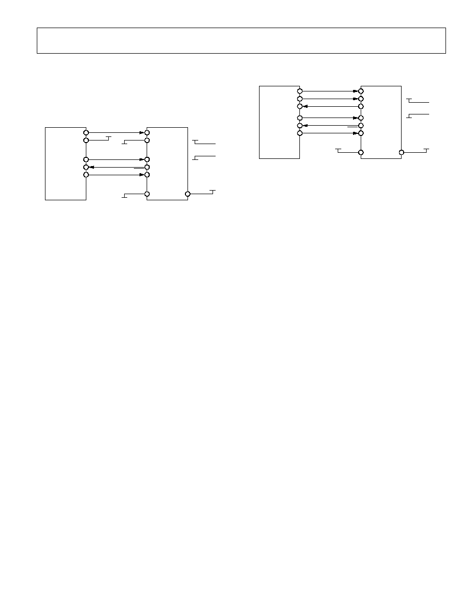
AD6654
Rev. 0 | Page 69 of 88
CONNECTING THE AD6654 SERIAL PORT TO A
BLACKFIN DSP
In SPI mode, the Blackfin DSP must act as a master to the
AD6654 by providing the SCLK. SDO is an open-drain output,
so that multiple slave devices can be connected together.
Figure 73 shows a typical connection.
SMODE
SCLK
SPISS
SRFS
AND
STFS
SCK
MOSI
MISO
SCS
SDO
SDI
PF2
MODE
BLACKFIN
(MASTER)
AD6654
(SLAVE)
PROGRAMMABLE FLAG
VDDIO
GND
05156-054
Figure 73. SPI Mode Serial Port Connection to Blackfin DSP
In SPORT mode, the Blackfin provides the SCLK, SRFS, and
STFS signals, as shown in Figure 74.
SMODE
SCLK
TFS
RFS
SRFS
STFS
SCK
DT
DR
SCS
SDO
SDI
PF2
MODE
BLACKFIN
AD6654
PROGRAMMABLE FLAG
VDDIO
GND
05156-055
Figure 74. SPORT Mode Serial Port Connections to Blackfin

AD6654
Rev. 0 | Page 70 of 88
MICROPORT
The microport on the AD6654 can be used for programming
the part, reading register values, and reading output data (I, Q,
and RSSI words).
Note that, at any given point in time, either the microport or the
serial port can be active, but not both. Some of the balls on the
package are shared between the microport and the serial port
and have dual functionality based on the SMODE pin. The
microport is selected by pulling the SMODE pin low (ground).
Both read and write operations can be performed using the
microport. The direct addressing scheme is used and any
internal register can be accessed using an 8-bit address. The
data bus can be either 8-bit or 16-bit as set by the chip I/O
access control register. Microport operation is synchronous to
CPUCLK, which must be supplied external to the AD6654 part.
CPUCLK should be less than CLK and 100 MHz.
The microport can operate in Intel mode (separate read and
write strobes) or in Motorola mode (single read/write strobe).
The MODE pin is used to select between Intel (INM, MODE =
0) and Motorola (MNM, MODE = 1) modes. Some AD6654
pins have dual functionality based on the MODE pin. Table 27
lists the pin functions for both modes.
Table 27. Microport Programming Pins
Pin Name
Intel Mode
Motorola Mode
RESET
RESET
RESET
SMODE
Logic 0
Logic 0
MODE
Logic 0
Logic 1
A[7:0] A[7:0] A[7:0]
D[15:0] D[15:0] D[15:0]
R/W (WR)
WR
R/W
DS (RD)
RD
DS
DTACK (RDY)
RDY
DTACK
CS
CS
CS
INTEL (INM) MODE
The programming port performs synchronous Intel-style reads
and writes on the positive edge of the CPUCLK input when
RESET is inactive (active low signal). The CPUCLK pin is
driven by the programming device (CPUCLK of DSP or
FPGA). During a write access, the A[7:0] address bus provides
the address for access, and the D[15:0] bus (D[7:0] if the 8-bit
data bus is used) is driven by the programming device. The data
bus is driven by the AD6654 during a read operation. Intel
mode uses separate read (RD) and write (WR) active low data
strobes to indicate both the type of access and the valid data for
that access.
The chip select (CS) is an active-low input that signals when an
access is active on its programming port pins. During an access,
the AD6654 drives RDY low to indicate that it is performing the
access. When the internal read or write access is complete, the
RDY pin is pulled high. Because the RDY pin is an open-drain
output with a weak internal pull-up resistor (70 k), an
external pull-up resistor is recommended (see the DDC Design
Notes section). Figure 10 and Figure 11 are the timing diagrams
for read and write cycles using the microport in INM mode.
For an asynchronous write operation in Intel (INM) mode, the
CPUCLK should be running. Set up the data and address buses.
Pull the WR signal low and then pull the CS signal low. The
RDY goes low to indicate that the access is taking place inter-
nally. When RDY goes high, the write cycle is complete and CS
can be pulled high to disable the microport.
For an asynchronous read operation on the Intel mode micro-
port, set up the address bus and three-state the data bus. Pull
the RD signal low and then pull the CS signal low. The RDY
goes low to indicate an internal access. When RDY goes low,
valid data is available on the data bus for read.
MOTOROLA (MNM) MODE
The programming port performs synchronous Motorola-style
reads and writes on the positive edge of CPUCLK when RESET
is inactive (active low signal). The A[7:0] bus provides the
address to access and the D[15:0] bus (D[7:0], if the 8-bit data
bus is used) is externally driven with data during a write (driven
by the AD6654 during a read). Motorola mode uses the R/W
line to indicate the type of access (Logic 1 = read, Logic 0 =
write), and the active low data strobe (DS) signal is used to
indicate valid data.
The chip select (CS) is an active-low input that signals when an
access is active on its programming port pins. When the read/
write cycle is complete, the AD6654 drives DTACK low. The
DTACK signal goes high again after either the CS or DS signal
is driven high. Because the DTACK pin is an open-drain output
with a weak internal pull-up resistor (70 k), an external pull-
up resistor is recommended (see the DDC Design Notes
section). Figure 12 and Figure 13 are the timing diagrams for
read and write cycles using the microport in MNM mode.
For an asynchronous write operation on the Motorola mode
microport, the CPUCLK should be running. Set up the data and
address buses. Pull the R/W and DS signals low and then pull
the CS signal low. The DTACK goes low after a few clock cycles
to indicate that the write access is complete and that CS can be
pulled high to disable the microport. For an asynchronous read
operation on the Motorola mode microport, set up the address
bus and three-state the data bus. Pull the RD signal low and
then pull the CS signal low. The DTACK goes low after a few
clock cycles to indicate that valid data is on the data bus.

AD6654
Rev. 0 | Page 71 of 88
ACCESSING MULTIPLE AD6654 DEVICES
If multiple AD6654 devices are on a single board, the microport
pins for these devices can be shared. In this configuration, a
single programming device (DSP, FPGA, or microcontroller)
can program all AD6654 devices connected to it.
Each AD6654 has four CHIPID pins that can be connected in
16 different ways. During a write/read access, the internal
circuitry checks to see if the CHIPID bits in the chip I/O access
control register (Address 0x02) are the same as the logic levels
of the CHIPID pins (hardwired to the part). If the CHIPID bits
and the CHIPID pins have the same value, then a write/read
access is completed; otherwise, the access is ignored.
To program multiple devices using the same microport control
and data buses, the devices should have separate CHIPID pin
configurations. A write/read access can be made only on the
intended chip; all other chips would ignore the access.

AD6654
Rev. 0 | Page 72 of 88
MEMORY MAP
READING THE MEMORY MAP TABLE
Each row in the memory map table has four address locations.
The memory map is roughly divided into four regions: global
register map (Address 0x00 to Address 0x0B), input port
register map (Address 0x0C to Address 0x67), channel register
map (Address 0x68 to Address 0xBB), and output port register
map (Address 0xBC to Address 0xE7). The channel register
map is shared by all six channels, and access to individual
channels is given by the channel I/O access control register
(Address 0x02).
In the memory map in Table 28, the addresses are given in the
right column. The column with the heading Byte 0 has the
address given in the right column. The column Byte 1 has the
address given by 1 more than the address listed in the right
column (address offset of 1). Similarly, the address offset for the
Byte 2 column is 2, and for the Byte 3 column is 3. For example,
the second row lists 0x04 as the address in the right column.
The pin synchronization configuration register has Address
0x04, the soft synchronization configuration register has
Address 0x05, and Address 0x06 and Address 0x07 are
reserved/open.
BIT FORMAT
All registers are in little-endian format. For example, if a register
takes 24 bits or three address locations, then the most signifi-
cant byte is at the highest address location and the least
significant byte is at a lowest address location. In all registers,
the least significant bit is Bit 0 and the most significant bit is
Bit 7. For example, the NCO frequency <31:0> register is
32 bits wide. Bit 0 (LSB) of this register is written at Bit 0 of
Address 0x70 and Bit 32 (MSB) of this register is written at
Bit 7 of Address 0x73.
When referring to a register that takes up multiple address
locations, it is referred to by the address location of the most
significant byte of the register. For example, the text reads,
"Port A dwell timer at Address 0x2A." Note that only the four
most significant bits of this register are at this location, and this
register also takes up Addresses 0x29 and 0x28.
OPEN LOCATIONS
All locations marked as open are currently not used. When
required, these locations should be written with 0s. Writing to
these locations is required only when part of an address location
is open (for example, Address 0x78). If the whole address
location is open (for example, Address 0x00), then this address
location does not need to be written. If the open locations are
read back using the microport or serial port, the readback value
is undefined (each bit can be independently 1 or 0), and these
bits have no significance.
If an address location has more than one register or has one
register with some open bits, then the order of these registers is
as given in Table 28. For example, Address 0x33 reads
Open <7:5>, Port A Signal Monitor <4:0>.
The open <7:5> is located at Bits <7:5> and the Port A signal
monitor <4:0> is located at Bits <4:0>.
Another example is Address 0x35:
Open <15:10>, Port A Upper Threshold <9:0>
Here, Bits <7:2> of Address 0x35 are open <15:10>. Bits <1:0>
of Address 0x35 and Bits <7:0> of Address 0x34 make up the
Port A upper threshold <9:0> register (Bit 1 of Address 0x35 is
the MSB of the Port A upper threshold register).
DEFAULT VALUES
Coming out of reset, some of the address locations (but not all)
are loaded with default values. When available, the default
values for the registers are given in the table. If the default value
is not listed, then the address location is in an undefined state
(Logic 0 or Logic 1) on RESET.
LOGIC LEVELS
In the explanation of various registers, "bit is set" is
synonymous with "bit is set to Logic 1" or "writing Logic 1 for
the bit." Similarly "clear a bit" is synonymous with "bit is set to
Logic 0" or "writing Logic 0 for the bit."
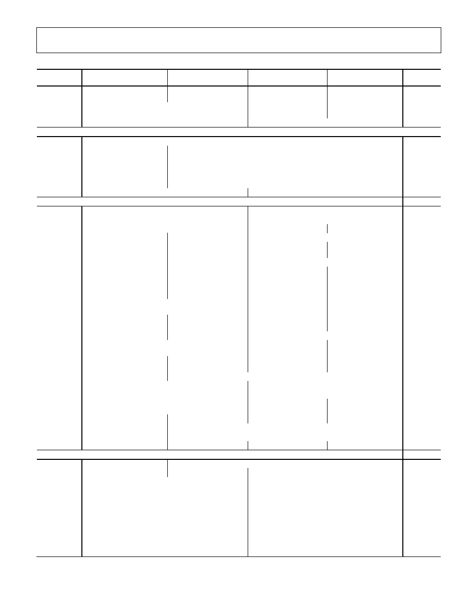
AD6654
Rev. 0 | Page 73 of 88
Table 28. Memory Map
8-Bit Hex
Address
Byte 3
Byte 2
Byte 1
Byte 0
8-Bit Hex
Address
0x03
Open <7:6>, Channel
Enable <5:0>
Open <7:6>, Channel I/O
Access Control <5:0>
Chip I/O Access Control
<7:0> (default 0x00)
Open <7:0>
0x00
0x07
Open <15:11>, Reserved <10:0> (default 0x06FC)
Soft Synchronization
Configuration <7:0>
Pin Synchronization
Configuration <7:0>
0x04
0x0B
Interrupt Mask <15:0>
Interrupt Status <15:0> (read only, default 0x00)
0x08
ADC Input Port Register Map-- Addresses 0x0C to 0x57
0x0F
ADC Input Control <31:0>
0x0C
0x13
Open <15:0>
ADC CLK Control <15:0> (default 0x0000)
0x10
0x4B
ADC Gain Control <7:0>
Open <23:20>, ADC Dwell Timer <19:0>
0x48
0x4F
Open <7:0>
ADC Power Monitor Period <23:0>
0x4C
0x53
Open <7:5>, ADC Signal
Monitor <4:0>
ADC Power Monitor Output <23:0>
0x50
0x57
Open <15:10>, ADC Lower Threshold <9:0>
Open <15:10>, ADC Upper Threshold <9:0>
0x54
Channel Register Map--Addresses 0x68 to 0xBB
0x6B
Open <15:0>
Open <15:9>, NCO Control <8:0>
0x68
0x6F
NCO Start Hold-Off Counter <15:0>
NCO Frequency Hold-Off Counter <15:0>
0x6C
0x73
NCO Frequency <31:0> (default 0x0000 0000)
0x70
0x77
Open <15:0>
NCO Phase Offset <15:0> (default 0x0000)
0x74
0x7B
Open <7:1>, CIC Bypass <0>
Open <7:5>, CIC
Decimation <4:0>
Open <7:5>, CIC Scale
Factor <4:0>
Open <7:4>, FIR-HB
Control <3:0>
0x78
0x7F
Open <15:0>
Open <15:13>, MRCF Control <12:0>
0x7C
0x83
Open <7:6>, MRCF
Coefficient 3 <5:0>
Open <7:6>, MRCF
Coefficient 2 <5:0>
Open <7:6>, MRCF
Coefficient 1 <5:0>
Open <7:6>, MRCF
Coefficient 0 <5:0>
0x80
0x87
Open <7:6>, MRCF
Coefficient 7 <5:0>
Open <7:6>, MRCF
Coefficient 6 <5:0>
Open <7:6>, MRCF
Coefficient 5 <5:0>
Open <7:6>, MRCF
Coefficient 4 <5:0>
0x84
0x8B
Open <15:13>, DRCF Control Register <12:0>
Open <7:6>, DRCF
Coefficient Offset <5:0>
Open <7>, DRCF Taps
<6:0>
0x88
0x8F
Open <15:0>
Open <7:6>, DRCF Final
Address <5:0>
Open <7:6>, DRCF Start
Address <5:0>
0x8C
0x93
Open<15:0>
Open<15:14>, DRCF Coefficient Memory <13:0>
0x90
0x97
Open <15:13>, CRCF Control Register <12:0>
Open <7:6>, CRCF
Coefficient Offset <5:0>
Open <7>, CRCF Taps
<6:0>
0x94
0x9B
Open <15:0>
Open <7:6>, CRCF Final
Address <5:0>
Open <7:6>, CRCF Start
Address <5:0>
0x98
0x9F
Open <7:0>
Open <23:20>, CRCF Coefficient Memory <19:0>
0x9C
0xA3
Open <15:11>, AGC Control Register <10:0>
AGC Hold-Off Register <15:0>
0xA0
0xA7
Open <15:12>, AGC Update Decimation <11:0>
Open <15:12>, AGC Signal Gain <11:0>
0xA4
0xAB
Open <15:12>, AGC Error Threshold <11:0>
Open <7:6>, AGC Average
Samples <5:0>
AGC Pole Location <7:0>
0xA8
0xAF
Open <7:0>
AGC Desired Level <7:0>
AGC Loop Gain2 <7:0>
AGC Loop Gain1 <7:0>
0xAC
0xB3
Open <7:0>
BIST I Path Signature Register <23:0> (read only)
0xB0
0xB7
Open <7:0>
BIST Q Path Signature Register <23:0> (read only)
0xB4
0xBB
Open <15:0>
BIST Control <15:0>
0xB8
Output Port Register Map--Addresses 0xBC to 0xE7
0xBF
Open <7:0>
Parallel Port Output Control <23:0>
0xBC
0xC3
Open <15:0>
Open <15:10>, Output Port Control <9:0>
0xC0
0xC7
AGC0, I Output <15:0> (read only)
AGC0, Q Output <15:0> (read only)
0xC4
0xCB
AGC1, I Output <15:0> (read only)
AGC1, Q Output <15:0> (read only)
0xC8
0xCF
AGC2, I Output <15:0> (read only)
AGC2, Q Output <15:0> (read only)
0xCC
0xD3
AGC3, I Output <15:0> (read only)
AGC3, Q Output <15:0> (read only)
0xD0
0xD7
AGC4, I Output <15:0> (read only)
AGC4, Q Output <15:0> (read only)
0xD4
0xDB
AGC5, I Output <15:0> (read only)
AGC5, Q Output <15:0> (read only)
0xD8
0xDF
Open <15:12>, AGC0 RSSI Output <11:0> (read only)
Open <15:12>, AGC1 RSSI Output <11:0> (read only)
0xDC
0xE3
Open <15:12>, AGC2 RSSI Output <11:0> (read only)
Open <15:12>, AGC3 RSSI Output <11:0> (read only)
0xE0
0xE7
Open <15:12>, AGC4 RSSI Output <11:0> (read only)
Open <15:12>, AGC5 RSSI Output <11:0> (read only)
0xE4

AD6654
Rev. 0 | Page 74 of 88
GLOBAL REGISTER MAP
Chip I/O Access Control Register <7:0>
<7>: Synchronous Microport Bit. When this bit is set, the
microport assumes that its control signals (such as R/W, DS,
and CS,) are synchronous to the CPUCLK. When cleared,
asynchronous control signals are assumed, and the microport
control signals are resynchronized with CPUCLK inside the
AD6654 part. Synchronous microport (when bit is set) has the
advantage of requiring a fewer number of clock cycles for
read/write access.
<6>: This bit is open.
<5:2>: Chip ID Bits. The chip ID bits are used to compare
against the chip ID input pins (CHIPID), enabling or disabling
I/O access for this specific chip. When more than one AD6654
part is sharing the microport, different CHIPID pins can be
used to differentiate among the parts. A particular part gives
I/O access only when the CHIPID pins have the same value as
these chip ID bits.
<1>: This bit is open.
<0>: Byte Mode Bit. The byte mode bit selects the bit width for
the microport operation. Table 29 shows details.
Table 29. Microport Data Bus Width Selection
Chip Access Control
Register <0>
Microport Data Bus Bit Width
0 (default)
8-bit mode, using D <7:0>
1
16-bit mode, using D <15:0>
Channel I/O Access Control Register <5:0>
These bits enable/disable the channel I/O access capability.
<5>: Channel 5 Access Bit. When the Channel 5 access bit is set
to Logic 1, any I/O write operation (from either the microport
or the serial port) that addresses a register located within the
channel register map updates the Channel 5 registers. Similarly,
for a read operation, the contents of the desired address in the
channel register map are output when this bit is set to Logic 1.
<4>: Channel 4 Access Bit. Similar to Bit <5> for Channel 4.
<3>: Channel 3 Access Bit. Similar to Bit <5> for Channel 3.
<2>: Channel 2 Access Bit. Similar to Bit <5> for Channel 2.
<1>: Channel 1 Access Bit. Similar to Bit <5> for Channel 1.
<0>: Channel 0 Access Bit. Similar to Bit <5> for Channel 0.
Note: If the access bits are set for more than one channel, during
write access all channels with access are written with the same
data. This is especially useful when more than one channel has
similar configurations. During a read operation, if more than
one channel has access, the read access is given to the channel
with the lowest channel number.
For example, if both Channel 4 and Channel 2 have access bits
set, then read access is given to Channel 2.
Channel Enable Register <5:0>
<5>: Channel 5 Enable Bit. When this bit is set, Channel 5 logic
is enabled. When this bit is cleared, Channel 5 is disabled and
the channel's logic does not consume any power. On power-up,
this bit comes up with Logic 0 and the channel is disabled. A
start sync does not start Channel 5, unless this bit is set before
issuing the start sync.
<4>: Channel 4 Enable Bit. Similar to Bit <5> for Channel 4.
<3>: Channel 3 Enable Bit. Similar to Bit <5> for Channel 3.
<2>: Channel 2 Enable Bit. Similar to Bit <5> for Channel 2.
<1>: Channel 1 Enable Bit. Similar to Bit <5> for Channel 1.
<0>: Channel 0 Enable Bit. Similar to Bit <5> for Channel 0.
Pin Synchronization Configuration <7:0>
<7>: Hop Synchronization Enable Bit. This bit is a global enable
for any hop synchronization involving SYNC pins. When this
bit is set, hop synchronization is enabled for all channels that
are programmed for pin synchronization. When this bit is
cleared, hop synchronization is not performed for any channel
that is programmed for pin synchronization.
<6>: Start Synchronization Enable Bit. This bit is a global enable
for any start synchronization involving SYNC pins. When this
bit is set, start synchronization is enabled for all channels that
are programmed for pin synchronization. When this bit is
cleared, start synchronization is not performed for any channel
that is programmed for pin synchronization.
<5>: First Sync Only Bit. When this bit is set, the NCO synchro-
nization logic recognizes only the first synchronization event as
valid. All other requests for synchronization events are ignored
as long as this bit is set. When cleared, all synchronization
events are acted upon.
<4>: Edge-Sensitivity Bit. When this bit is set, the rising edge on
the SYNC pin(s) is detected as a synchronization event (edge-
sensitive detection). When cleared, Logic 1 on the SYNC pin(s)
is detected as a synchronization event (level-sensitive
detection).
<3>: Enable Synchronization from SYNC3 Bit. When this bit is
set, the SYNC3 pin can be used for synchronization. When this
bit is cleared, the SYNC3 pin is ignored. This is a global enable
for all SYNC pins, and each individual channel selects which
pin it listens to.

AD6654
Rev. 0 | Page 75 of 88
<2>: Enable Synchronization from SYNC2 Bit. Similar to
Bit <3> for the SYNC2 pin.
<1>: Enable Synchronization from SYNC1 Bit. Similar to
Bit <3> for the SYNC1 pin.
<0>: Enable Synchronization from SYNC0 Bit. Similar to
Bit <3> for the SYNC0 pin.
Soft Synchronization Configuration <7:0>
<7>: Soft Hop Synchronization Enable Bit. When this bit is set,
hop synchronization is enabled for all channels selected using
Bit 5 through Bit 0. When this bit is cleared, hop synchroniza-
tion is not performed for any channels selected using Bit 5 to
Bit 0.
<6>: Soft Start Synchronization Enable Bit. When this bit is set,
start synchronization is enabled for all channels selected using
Bit 5 through Bit 0. When this bit is cleared, start synchronization
is not performed for any channels selected using Bit 5 to Bit 0.
Bits <5:0> form the SOFT_SYNC control bits. These bits can be
written to by the controller to initiate the synchronization of a
selected channel.
<5>: Soft Sync Channel 5 Enable Bit. When this bit is set, it
enables Channel 5 to receive a hop sync or start sync, as defined
by Bit 7 and Bit 6, respectively. When cleared, Channel 5 does
not receive any soft sync.
<4>: Soft Sync Channel 4 Enable Bit. Similar to Bit <5> for
Channel 4.
<3>: Soft Sync Channel 3 Enable Bit. Similar to Bit <5> for
Channel 3.
<2>: Soft Sync Channel 2 Enable Bit. Similar to Bit <5> for
Channel 2.
<1>: Soft Sync Channel 1 Enable Bit. Similar to Bit <5> for
Channel 1.
<0>: Soft Sync Channel 0 Enable Bit. Similar to Bit <5> for
Channel 0.
<10:0>: Reserved.
<10:9>: Reserved. This bit must be written with Logic 1.
<8:0>: Reserved. This bit must be written with Logic 0.
Interrupt Status Register <15:0>
This register is read only.
<15>: AGC5 RSSI Update Interrupt Bit. If the AGC5 update
interrupt enable bit is set, this bit is set by the AD6654
whenever AGC5 updates a new RSSI word (the new word
should be different from the previous word). If the AGC5
update interrupt enable bit is cleared, then this bit is not set (not
updated). An interrupt is not generated in this case.
Note: For Bits <15:10>, no interrupt is generated, if the new
RSSI word is the same as the previous RSSI word.
<14>: AGC4 RSSI Update Interrupt Bit. Similar to Bit <15> for
the AGC4.
<13>: AGC3 RSSI Update Interrupt Bit. Similar to Bit <15> for
the AGC3.
<12>: AGC2 RSSI Update Interrupt Bit. Similar to Bit <15> for
the AGC2.
<11>: AGC1 RSSI Update Interrupt Bit. Similar to Bit <15> for
the AGC1.
<10>: AGC0 RSSI Update Interrupt Bit. Similar to Bit <15> for
the AGC0.
<9>: Channel 5 Data Ready Interrupt Bit. This bit is set to
Logic 1 whenever the channel BIST signature registers are
loaded with data. The conditions required for setting this bit are
that the channel BIST signature registers are programmed for
BIST signature generation and the Channel 5 data ready enable
bit in the interrupt enable register is cleared. If the Channel 5
data ready enable bit in the interrupt enable register is set, the
AD6654 does not set this bit on signature generation and an
interrupt is not generated.
<8>: Channel 4 Data Ready Interrupt Bit. Similar to Bit <9> for
Channel 4.
<7>: Channel 3 Data Ready Interrupt Bit. Similar to Bit <9> for
Channel 3.
<6>: Channel 2 Data Ready Interrupt Bit. Similar to Bit <9> for
Channel 2.
<5>: Channel 1 Data Ready Interrupt Bit. Similar to Bit <9> for
Channel 1.
<4>: Channel 0 Data Ready Interrupt Bit. Similar to Bit <9> for
Channel 0.
<3>: Reserved. This bit must be written with Logic 0.
<2>: ADC Port Power Monitoring Interrupt Bit. This bit is set
by the AD6654 whenever the ADC port power monitor
interrupt enable bit is set and the ADC port power monitor
timer runs out (end of the ADC port power monitor period). If
the ADC port power monitor interrupt enable bit is cleared, the
AD6654 does not set this bit and does not generate an interrupt.
<1>: Reserved. This bit must be written with Logic 0.
<0>: Reserved. This bit must be written with Logic 0.

AD6654
Rev. 0 | Page 76 of 88
Interrupt Enable Register <15:0>
<15>: AGC5 RSSI Update Enable Bit. When this bit is set, the
AGC5 RSSI update interrupt is enabled, allowing an interrupt
to be generated when the RSSI word is updated.
When this bit is cleared, an interrupt cannot be generated for
this event. Also, see the Interrupt Status Register <15:0> section.
<14>: AGC4 RSSI Update Enable Bit. Similar to Bit <15> for
the AGC4.
<13>: AGC3 RSSI Update Enable Bit. Similar to Bit <15> for
the AGC3.
<12>: AGC2 RSSI Update Enable Bit. Similar to Bit <15> for
the AGC2.
<11>: AGC1 RSSI Update Enable Bit. Similar to Bit <15> for
the AGC1.
<10>: AGC0 RSSI Update Enable Bit. Similar to Bit <15> for
the AGC0.
<9>: Channel 5 Data Ready Enable Bit. When this bit is set, the
Channel 5 data ready interrupt is enabled, allowing an interrupt
to be generated when Channel 5 BIST signature registers are
updated. When this bit is cleared, an interrupt cannot be
generated for this event.
<8>: Channel 4 Data Ready Enable Bit. Similar to Bit <9> for
Channel 4.
<7>: Channel 3 Data Ready Enable Bit. Similar to Bit <9> for
Channel 3.
<6>: Channel 2 Data Ready Enable Bit. Similar to Bit <9> for
Channel 2.
<5>: Channel 1 Data Ready Enable Bit. Similar to Bit <9> for
Channel 1.
<4>: Channel 0 Data Ready Enable Bit. Similar to Bit <9> for
Channel 0.
<3>: Reserved. This bit must be written with Logic 0.
<2>: ADC Port Power Monitoring Enable Bit. When this bit is
set to Logic 1, the ADC port power monitoring interrupt is
enabled, allowing an interrupt to be generated when ADC port
power monitoring registers are updated. When set to Logic 1,
the ADC port power monitoring interrupt is disabled.
<1>: Reserved. This bit must be written with Logic 0.
<0>: Reserved. This bit must be written with Logic 0.
INPUT PORT REGISTER MAP
ADC Input Control Register <27:0>
These bits are general control bits for the ADC input logic.
<27>: PN Active Bit. When this bit is set, the pseudorandom
number generator is active. When this bit is cleared, the PN
generator is disabled and the seed is set to its default value.
<26>: EXP Lock Bit. When this bit is set along with the PN
active bit, then the EXP signal for pseudorandom input is
locked to 000 (giving full-scale input). When this bit is cleared,
EXP bits for pseudorandom input are randomly generated input
data bits.
<25> Reserved. This bit must be written with Logic 0.
<24> Reserved. This bit must be written with Logic 0.
<23:20>: Channel 5 Cross Bar Mux Select Bits. These bits select
the source of input data for Channel 5. See Table 30.
Table 30. Input Data Source Selection
Cross Bar Mux Select Bits
Configuration
0010
ADC port drives input (real)
0100
PN sequence drives input (real)
<19>: Reserved. This bit must be written with Logic 0.
<18:16>: Channel 4 Cross Bar Mux Select Bits. Similar to bits
<22:20>, but for Channel 4.
<15>: Reserved. This bit must be written with Logic 0.
<14:12>: Channel 3 Cross Bar Mux Select Bits. Similar to
Bits <22:20> for Channel 3.
<11>: Reserved. This bit must be written with Logic 0.
<10:8>: Channel 2 Cross Bar Mux Select Bits. Similar to
Bits <22:20> for Channel 2.
<7>: Reserved. This bit must be written with Logic 0.
<6:4>: Channel 1 Cross Bar Mux Select Bits. Similar to
Bits <22:20> for Channel 1.
<3>: Reserved. This bit must be written with Logic 0.
<2:0>: Channel 0 Cross Bar Mux Select Bits. Similar to
Bits <22:20> for Channel 0.
ADC CLK Control Register <11:0>.
These bits control the ADC clocks and internal PLL clock.
<11>: Reserved. This bit must be written with Logic 0.

AD6654
Rev. 0 | Page 77 of 88
<10>: ADC Port CLK Invert Bit. When this bit is set, the
inverted ADC port clock is used to register ADC input data into
the part. When this bit is cleared, the clock is used as is, without
any inversion or phase change.
<9>: Reserved. This bit must be written with Logic 0.
<8>: Reserved. This bit must be written with Logic 0.
<7:6>: ADC Pre PLL Clock Divider Bits.: These bits control the
PLL clock divider. The PLL clock is derived from the ADC data
port CLK.
Table 31. Divide-by Values for PLL Clock Divider Bits
PLL Clock Divider Bits <12:11>
Divide-by Value
00
Divide by 1, bypass
01
Divide by 2
10
Divide by 4
11
Divide by 8
<5:1>: PLL Clock Multiplier Bits. These bits control the PLL
clock multiplier. The output of the PLL clock divider is
multiplied with the binary value of these bits. Valid range for
the multiplier is from 4 to 20. A value outside this range powers
down the PLL, resulting in the PLL clock being the same as the
ADC data port CLK.
<0>: This bit is open.
ADC Port Gain Control <7:0>
<7>: This bit is open.
<6:1>: This 6-bit word specifies the relinearization pipe delay to
be used in the ADC input gain control block. The decimal
representation of these bits is the number of input clock cycle
pipeline delays between the external EXP data output and the
internal application of relinearization based on EXP.
<0>: Gain Control Enable Bit. This bit controls the configura-
tion of the EXP<2:0> bits for the ADC input port. When the
gain control enable bit is Logic 1, the EXP<2:0> bits are
configured as outputs. When this bit is cleared, the EXP<2:0>
bits are inputs.
ADC Port Dwell Timer <19:0>
This register is used to set the dwell time for the gain control
block. When the gain control block is active and detects a
decrease in the signal level below the lower threshold value
(programmable), a dwell-time counter is initiated to provide
temporal hysteresis. Doing so prevents the gain from being
continuously switched. Note that the dwell timer is turned on
only after a drop below the lower threshold is detected in the
signal level.
ADC Port Power Monitor Period <23:0>
This register is used in the power monitoring logic to set the
period of time for which ADC input data is monitored. This
value represents the monitor period in number of ADC port
clock cycles.
ADC Port Power Monitor Output <23:0>
This register is read only and contains the current status of the
power monitoring logic output. The output is dependent on the
power monitoring mode selected. When the power monitor
block is enabled, this register is updated at the end of each
power monitor period. This register is updated even if an
interrupt signal is not generated.
ADC Port Upper Threshold <9:0>
This register serves the dual purpose of specifying the upper
threshold value in the gain control block and in the power
monitoring block, depending on which block is active. ADC
port input data having a magnitude greater than this value
triggers a gain change in the gain control block. ADC port input
data having a magnitude greater than this value is monitored in
the power monitoring block (in peak detect or threshold
crossing mode). The value of the register is compared with the
absolute magnitude of the input port data.
ADC Port Lower Threshold <9:0>
This register is used in the gain control block and represents the
magnitude of the lower threshold for ADC port input data. Any
ADC input data having a magnitude below the lower threshold
initiates the dwell time counter. The value of the register is
compared with the absolute magnitude of the input port data.
ADC Port Signal Monitor <4:0>
This register controls the functions of the power monitoring
block.
<4>: Disable Power Monitor Period Timer Bit. When this bit is
set, the power monitor period timer no longer controls the
update of the power monitor holding register. A user read to the
power monitor holding register updates this register. When this
bit is cleared, the power monitor period register controls the
timer and, therefore, controls the update rate of the power
monitor holding register.
<3>: Clear-on-Read Bit. When this bit is set, the power monitor
holding register is cleared every time this register is read. This
bit controls whether the power monitoring function is cleared
after a read of the power monitor period register. If this bit is
set, the monitoring function is cleared after the read. If this bit
is Logic 0, the monitoring function is not cleared. This bit is a
don't care bit, if the disable integration counter bit is cleared.
AD6654
Rev. 0 | Page 78 of 88
<2:1>: Monitor Function Select Bits. Table 32 describes the
function of these bits.
Table 32. Monitor Function Select Bits
Monitor Function Select
Function Enabled
00
Peak detect mode
01
Mean power monitor mode
10
Threshold crossing mode
11
Invalid selection
<0>: Monitor Enable Bit. When this bit is set, the power
monitoring function is enabled and operates as selected by Bit 2
to Bit 1 of the signal monitor register. When this bit is cleared,
the power monitoring function is disabled and the signal
monitor register bits <2:1> are don't care bits. These bits default
to 0 on power-up.
CHANNEL REGISTER MAP
Channel control registers are common to all six channels, and
access to specific channels is determined by the channel I/O
access register (Address 0x02).
NCO Control <15:0>
These bits control the NCO operation.
<8:7>: NCO Sync Start Select Bits. These bits determine which
SYNC input pin is used by this channel for a start synchroniza-
tion operation. Table 33 describes the selection.
Table 33. Sync Start Select Bits
NCO Control <8:7>
SYNC Pin Used for Start
Synchronization
00
SYNC0
01
SYNC1
10
SYNC2
11
SYNC3
<6:5>: NCO Sync Hop Select Bits. These bits determine which
SYNC input pin is used by this channel for a hop synchroniza-
tion operation. Table 34 describes the selection.
Table 34. Sync Hop Select Bits
NCO Control <6:5>
SYNC Pin Used for Hop
Synchronization
00
SYNC0
01
SYNC1
10
SYNC2
11
SYNC3
<4>: This bit is open.
<3>: NCO Bypass Bit. When this bit is set, the NCO is bypassed
and shuts down for power savings. This bit can be used for
power savings, when NCO frequency of dc or 0 Hz is required.
When this bit is cleared, the NCO operates as programmed.
<2>: Clear NCO Accumulator Bit. When this bit is set, the clear
NCO accumulator bit synchronously clears the phase
accumulator on all frequency hops in this channel. When this
bit is cleared, the accumulator is not cleared and phase
continuous hops are implemented.
<1>: Phase Dither Enable Bit. When this bit is set, phase
dithering in the NCO is enabled. When this bit is cleared, phase
dithering is disabled.
<0>: Amplitude Dither Enable Bit. When this bit is set,
amplitude dithering in the NCO is enabled. When this bit is
cleared, amplitude dithering is disabled.
Channel Start Hold-Off Counter <15:0>
When a start synchronization (software or hardware) occurs on
the channel, the value in this register is loaded into a down-
counter. When the counter has finished counting down to 0, the
channel operation is started.
NCO Frequency Hop Hold-Off Counter <15:0>
When a hop sync occurs, a counter is loaded with the NCO
frequency hold-off register value. The 16-bit counter starts
counting down. When it reaches 0, the new frequency value in
the shadow register is written to the NCO frequency register.
(See the NCO Frequency Hold-Off Register section.)
NCO Frequency <31:0>
The value in this register is used to program the NCO tuning
frequency. The value to be programmed is given by the
following equation:
32
2
_
×
=
CLK
FREQUENCY
NCO
Register
Frequency
NCO
where:
NCO_FREQUENCY
is the desired NCO tuning frequency.
CLK
is the ADC clock rate.
The value given by the equation should be loaded into the
register in binary format.
NCO Phase Offset <15:0>
The value in the register is loaded into the phase accumulator of
the NCO block every time a start sync or hop sync is received
by the channel. This allows individual channels to be started
with a known nonzero phase. The NCO phase offset is not
loaded on a hop sync, if Bit <2> of the NCO control register
(clear phase accumulator on hop) is cleared. This NCO offset
register value is interpreted as a 16-bit unsigned integer. A
0x0000 in this register corresponds to a 0 radian offset, and a
0xFFFF corresponds to an offset of 2 (1 - 1/(2
16
)) radians.
CIC Bypass <0>
When this bit is set, the entire CIC filter is bypassed. The output
of CIC filter is driven straight from the input without any
change. When this bit is cleared, the CIC filter operates in
normal mode as programmed. Writing Logic 1 to this bit
disables both the CIC decimation and CIC scaling operations.
AD6654
Rev. 0 | Page 79 of 88
CIC Decimation <4:0>
This 5-bit word specifies the CIC filter decimation value
minus 1. A value of 0x00 is a decimation of 1 (bypass), and
0x1F is a decimation of 32. Writing a value of 0 in this register
bypasses CIC filtering, but does not bypass the CIC scaling
operation.
CIC Scale Factor <4:0>
This 5-bit word specifies the CIC filter scale factor used to
compensate for the gain provided by the CIC filter. The
recommended value is given by the following equation:
5
))
(
log
5
(
2
-
×
=
CIC
M
ceil
Register
Scale
CIC
where:
M
CIC
is the decimation rate of the CIC (one more than the value
in the CIC decimation register).
ceil
operation gives the closest integer greater than or equal to
the argument.
The valid range for this register is decimal 0 to 20.
FIR-HB Control <3:0>
<3>: FIR1 Enable Bit. When this bit is set, the FIR1 fixed
coefficient filter is enabled. When cleared, FIR1 is bypassed.
<2>: HB1 Enable Bit. When this bit is set, the HB1 half-band
filter is enabled. When cleared, HB1 is bypassed.
<1>: FIR2 Enable Bit. When this bit is set, the FIR2 fixed
coefficient filter is enabled. When cleared, FIR2 is bypassed.
<0>: HB2 Enable Bit. When this bit is set, the HB2 half-band
filter is enabled. When cleared, HB2 is bypassed.
MRCF Control Register <12:0>
<12:10>: MRCF Data Select Bits. These bits are used to select
the input source for the MRCF filter. Each MRCF filter can be
driven by output from the HB2 filter of any channel independ-
ently. Table 35 shows the selections available.
Table 35. MRCF Data Select Bits
MRCF Data Select<2:0>
MRCF Input Source
000
MRCF input taken from Channel 0
001
MRCF input taken from Channel 1
010
MRCF input taken from Channel 2
011
MRCF input taken from Channel 3
1x0
MRCF input taken from Channel 4
1x1
MRCF input taken from Channel 5
<9>: Interpolating Half-Band Enable Bit. When this bit is set,
the interpolating half-band filter, driven by the output of the
CRCF block, is enabled. When cleared, the interpolating half-
band filter is bypassed, and its output is the same as its input.
The interpolating half-band filter doubles the data rate.
<8>: This bit is open.
<7>: Half-Rate Bit. When this bit is set, the MRCF filter
operates using half the PLL clock rate. This is used for power
savings when there is sufficient time to complete MRCF
filtering using only half the PLL clock rate. When this bit is
cleared, the MRCF filter operates at the full PLL clock rate. See
the Mono-Rate RAM Coefficient Filter (MRCF) section.
<6:4>: MRCF Number of Taps Bits. This 3-bit word should be
written with one less than the number of taps that are calculated
by the MRCF filter. The filter length is given by the decimal
value of this register plus 1. A value of 0 represents a 1-tap filter
and maximum value of 7 represents an 8-tap filter.
<3:2>: MRCF Scale Factor Bits. The output of the MRCF filter is
scaled according to the value of these bits. Table 36 describes
the attenuation corresponding to each setting.
Table 36. MRCF Scale Factor
MRCF Scale<1:0>
Scale Factor
00
18.06 dB attenuation (left-shift 3 bits)
01
12.04 dB attenuation (left-shift 2 bits)
10
6.02 dB attenuation (left-shift 1 bit)
11
No scaling (0 dB)
<1>: This bit is open.
<0>: MRCF Bypass Bit. When this bit is set, the MRCF filter is
bypassed and, therefore, the output of the MRCF is the same as
its input. When this bit is cleared, the MRCF has normal
operation as programmed by its control register.
MRCF COEFFICIENT MEMORY
The MRCF coefficient memory consists of eight coefficients,
each six bits wide. The memory extends from Address 0x80 to
Address 0x87. The coefficients should be written in twos
complement format.
DRCF Control Register <11:0>
<11>: DRCF Bypass Bit. When this bit is set, the DRCF filter is
bypassed and, therefore, its output is the same as its input.
When this bit is cleared, the DRCF has normal operation as
programmed by the rest of this control register.
<10>: Symmetry Bit. When this bit is set, it indicates that the
DRCF is implementing a symmetrical filter and only half the
impulse response needs to be written into the DRCF coefficient
RAM. When this bit is cleared, the filter is asymmetrical and
complete impulse response of the filter should be written to the
coefficient RAM. When this filter is symmetrical, it can imple-
ment up to 128 filter taps.
<9:8>: DRCF Multiply Accumulate Scale Bits. The output of the
DRCF filter is scaled according to the value of these bits.
Table 37 lists the attenuation corresponding to each setting.

AD6654
Rev. 0 | Page 80 of 88
Table 37. DRCF Multiply Accumulate Scale Bits
DRCF Scale <1:0>
Scale Factor
00
18.06 dB attenuation (left-shift 3 bits)
01
12.04 dB attenuation (left-shift 2 bits)
10
6.02 dB attenuation (left-shift 1 bit)
11
No scaling (0 dB)
<7:4>: DRCF Decimation Rate. This 4-bit word should be
written with one less than the decimation rate of the DRCF
filter. A value of 0 represents a decimation rate of 1 (no rate
change), and the maximum value of 15 represents a decimation
of 16. Filtering can be implemented regardless of the
decimation rate.
<3:0>: DRCF Decimation Phase Bits. This 4-bit word represents
the decimation phase used by the DRCF filter. The valid range
is 0 up to M
DRCF
- 1, where M
DRCF
is the decimation rate of the
DRCF filter. This word is primarily used for synchronization of
multiple channels of the AD6654, when more than one channel
is used for filtering one signal (one carrier).
DRCF Coefficient Offset <7:0>
This register is used to specify which section of the 64-word
coefficient memory is used for a filter. It can be used to select
between multiple filters that are loaded into memory and
referenced by this pointer. This register is shadowed, and the
filter pointer is updated every time a new filter is started. This
allows the coefficient offset to be written even while a filter is
being computed without disturbing operation. The next sample
comes out of the DRCF with the new filter.
DRCF Taps <6:0>
This register is written with one less than the number of taps
that are calculated by the DRCF filter. The filter length is given
by the decimal value of this register plus 1. A value of 0
represents a 1-tap filter, and a value of 0x28 (40 decimal)
represents a 41-tap filter.
DRCF Start Address <5:0>
This register is written with the starting address of the DRCF
coefficient memory to be updated.
DRCF Final Address <5:0>
This register is written with the ending address of the DRCF
coefficient memory to be updated.
DRCF Coefficient Memory <13:0>
DRCF Memory. This memory consists of 64 words, and each
word is 14 bits wide. The data written to this memory space is
expected to be 14-bit, twos complement format. See the
Decimating RAM Coefficient Filter (DRCF) section for the
method to program the coefficients into the coefficient
memory.
CRCF Control Register <11:0>
<11>: CRCF Bypass Bit. When this bit is set, the DRCF filter is
bypassed and, therefore, its output is the same as its input.
When this bit is cleared, the CRCF has normal operation as
programmed by its control register.
<10>: Symmetry Bit. When this bit is set, it indicates that the
CRCF is implementing a symmetrical filter and only half the
impulse response needs to be written into the CRCF coefficient
RAM. When this bit is cleared, the filter is asymmetrical and
the complete impulse response of the filter should be written
into the coefficient RAM. When this filter is symmetrical, it can
implement up to 128 filter taps.
<9:8>: CRCF Multiply Accumulate Scale Bits. The output of the
CRCF filter is scaled according to the value of these bits.
Table 38 lists the attenuation corresponding to each setting.
Table 38. CRCF Multiply Accumulate Scale Bits
CRCF Scale<1:0>
Scale Factor
00
18.06 dB attenuation (left-shift 3 bits)
01
12.04 dB attenuation (left-shift 2 bits)
10
6.02 dB attenuation (left-shift 1 bit)
11
No scaling (0 dB)
<7:4>: CRCF Decimation Rate. This 4-bit word should be writ-
ten with one less than the decimation rate of the CRCF filter. A
value of 0 represents a decimation rate of 1 (no rate change) and
the maximum value of 15 represents a decimation of 16.
Filtering operation is done regardless of the decimation rate.
<3:0>: CRCF Decimation Phase. This 4-bit word represents the
decimation phase used by the CRCF filter. The valid range is 0
to MCRCF - 1, where MCRCF is the decimation rate of the
CRCF filter. This word is primarily used for synchronization of
multiple channels of the AD6654, when more than one channel
is used for filtering one signal (one carrier).
CRCF Coefficient Offset <5:0>
This register is used to specify which section of the 64-word
coefficient memory is used for a filter. It can be used to select
between multiple filters that are loaded into memory and
referenced by this pointer. This register is shadowed, and the
filter pointer is updated every time a new filter is started. This
allows the coefficient offset to be written even while a filter is
being computed without disturbing operation. The next sample
comes out of the CRCF with the new filter.
CRCF Taps <6:0>
This register is written with one less than the number of taps
that are calculated by the CRCF filter. The filter length is given
by the decimal value of this register plus 1. A value of 0 repre-
sents a 1-tap filter, and a value of 0x28 (40 decimal) represents a
41-tap filter.

AD6654
Rev. 0 | Page 81 of 88
CRCF Coefficient Memory
CRCF Memory. This memory has 64 words that have 20 bits
each. The memory contains the CRCF filter coefficients. The
data written to this memory space is 20-bit in twos complement
format. See the Channel RAM Coefficient Filter (CRCF) section
for the method to program the coefficients into the coefficient
memory.
AGC Control Register <10:0>
<10>: Channel Sync Select Bit. When this bit is set, the AGC
uses the sync signal from the channel for its synchronization.
When this bit is cleared, the SYNC pin used for synchronization
is defined by Bit 9 to Bit 8 of this register.
<9:8>: SYNC Pin Select Bits. When Bit 10 of this register is
cleared, these bits specify the SYNC pin used by AGC for
synchronization. These bits are don't care when Bit 10 of the
AGC control register is set to Logic 1.
Table 39. SYNC Pin Select Bits
AGC Control Bits <9:8>
SYNC Pin Used by AGC
00
SYNC0
01
SYNC1
10
SYNC2
11
SYNC3
<7:5>: AGC Word Length Control Bits. These bits define the
word length of the AGC output. The output word can be 4 to 8,
10, 12, or 16 bits wide. Table 40 shows the possible selections.
Table 40. AGC Word Length Control Bits
AGC Control Bits <7:5>
Output Word Length (Bits)
000
16
001
12
010
10
011
8
100
7
101
6
110
5
111
4
<4>: AGC Mode Bit. When this bit is cleared, the AGC operates
to maintain a desired signal level. When this bit is set, it
operates to maintain a constant clipping level. See the
Automatic Gain Control section for details about these modes.
<3>: AGC Sync Now Bit. This bit is used to synchronize a
particular AGC, regardless of the channel, through the
programming ports (microport or serial port). When this bit is
set, the AGC block updates a new output sample (RSSI sample)
and starts working toward a new update sample.
<2>: Initialize on Sync Bit. This bit is used to determine
whether or not the AGC should initialize on a sync. When this
bit is set, during a synchronization the CIC filter is cleared and
new values for CIC decimation, number of averaging samples,
CIC scale, Signal Gain K, and the Pole P parameter are loaded.
When Bit 2 = 0, the above-mentioned parameters are not
updated, and the CIC filter is not cleared. In both cases, an
AGC update sample is output from the CIC filter and the
decimator starts operating towards the next output sample
whenever a sync occurs.
<1>: First Sync Only. This bit is used to ignore repetitive
synchronization signals. In some applications, the synchroniza-
tion signal occurs periodically. If this bit is cleared, each
synchronization request resynchronizes the AGC. If this bit is
set, only the first occurrence causes the AGC to synchronize
and updates the AGC gain values periodically, depending on
the decimation factor of the AGC CIC filter.
<0>: AGC Bypass Bit. When this bit is set, the AGC section is
bypassed. The N-bit representation from the interpolating half-
band filters is still reduced to a lower bit width representation as
set by Bit 7 to Bit 5 of the AGC control register. A truncation at
the output of the AGC accomplishes this task.
AGC Hold-Off Register <15:0>
The AGC hold-off counter is loaded with the value written to
this address when either a soft sync or pin sync comes into the
channel. The counter begins counting down. When it reaches 1,
a sync is sent to the AGC. This sync might or might not initial-
ize the AGC, as defined by the control word. The AGC loop is
updated with a new sample from the CIC filter whenever a sync
occurs. If this register is Logic 1, the AGC is immediately
updated when the sync occurs. If this register is Logic 0, the
AGC cannot be synchronized.
AGC Update Decimation <11:0>
This 12-bit register sets the AGC decimation ratio from 1 to
4096. An appropriate scaling factor should be set to avoid loss
of bits. The decimation ratio is given by the decimal value of the
AGC update decimation<11:0> register contents plus 1, that is,
12'0x000 describes a decimation ratio of 1, and 12'0xFFF
describes a decimation ratio of 4096.
AGC Signal Gain <11:0>
This register is used to set the initial value for a signal gain used
in the gain multiplier. This 12-bit value sets the initial signal
gain in the range of 0 dB and 96.296 dB in steps of 0.024 dB.
Initial signal gain (SG) in dB should be converted to a register
setting using the following formula:
×
=
256
)
2
(
log
20
10
SG
round
Value
Register
AGC Error Threshold <11:0>
This 12-bit register is the comparison value used to determine
which loop gain value (K
1
or K
2
) to use for optimum operation.
When the magnitude-of-error signal is less than the AGC error
threshold value, then K
1
is used; otherwise, K
2
is used. The word

AD6654
Rev. 0 | Page 82 of 88
format of the AGC error threshold register is four bits to the left
of the binary point and eight bits to the right.
See the Automatic Gain Control section for details.
256
)
2
(
log
20
10
×
=
Threshold
Error
round
Value
Register
AGC Average Samples <5:0>
This 6-bit register contains the scale used for the CIC filter and
the number of power samples to be averaged before being sent
to the CIC filter.
<5:2>: CIC Scale. This 4-bit word defines the scale used for the
CIC filter. Each increment of this word increases the CIC scale
by 6.02 dB.
<1:0>: Number of AGC Average Samples. This defines the
number of samples to be averaged before they are sent to the
CIC decimating filter. See Table 41.
Table 41. Number of AGC Average Samples
AGC Average Samples <1:0>
Number of Samples Taken
00
1
01
2
10
3
11
4
AGC Pole Location <7:0>
This 8-bit register is used to define P, the open-loop filter pole
location. Its value can be set from 0 to 0.996 in steps of 0.0039.
This value of P is updated in the AGC loop each time the AGC
is initialized. This open-loop pole location directly impacts the
closed-loop pole locations, as explained in the Automatic Gain
Control section.
AGC Desired Level <7:0>
This register contains the desired signal level or desired clipping
level, depending on operational mode. This desired request
level (R) can be set in dB from 0 to 23.99 in steps of 0.094 dB.
The request level (R) in dB should be converted to a register
setting using the following formula:
×
=
64
)
2
(
log
20
10
R
round
Value
Register
AGC Loop Gain 2 <7:0>
This 8-bit register is used to define K
2
, the second possible
open-loop gain. Its value can be set from 0 to 0.996 in steps of
0.0039. This value of K
2
is updated each time the AGC is
initialized. When the magnitude-of-error signal in the loop is
greater than the AGC error threshold, then K
2
is used by the
loop. K
2
is updated only when the AGC is initialized.
AGC Loop Gain 1 <7:0>
This 8-bit register is used to define K
1
, the open-loop gain. Its
value can be set from 0 to 0.996 in steps of 0.0039. This value of
K is updated in the AGC loop each time the AGC is initialized.
When the magnitude-of-error signal in the loop is less than the
AGC error threshold, then K
1
is used by the loop. K
1
is updated
only when the AGC is initialized.
I Path Signature Register <15:0>
This 16-bit signature register is for the I path of the channel
logic. The signature register records data on the networks that
leave the channel logic, just before entering the second data
router.
Q Path Signature Register <15:0>
This 16-bit signature register is for the Q path of the channel
logic. The signature register records data on the networks that
leave the channel logic, just before entering the second data
router.
BIST Control <15:0>
<15>: Disable Signature Generation Bit. When this bit is active
high, the signature registers do not produce a pseudorandom
output value, but instead directly load the 24-bit input data.
When this bit is cleared, the signature register produces a
pseudorandom output for every clock cycle that it is active. See
the User-Configurable Built-In Self-Test (BIST) section for
details.
<14:0>: BIST Timer Bits. The <14:0> bits of this register form a
15-bit word that is loaded into the BIST timer. After loading the
BIST timer, the signature register is enabled for operation while
the timer is actively counting down. See the User-Configurable
Built-In Self-Test (BIST) section for details.
OUTPUT PORT REGISTER MAP
This part of the memory map deals with the output data and
controls for parallel output ports.
Parallel Port Output Control <23:0>
<23>: Port C Append RSSI Bit. When this bit is set, an RSSI
word is appended to every I/Q output sample, regardless of
whether the RSSI word is updated in the AGC. When this bit is
cleared, an RSSI word is appended to an I/Q output sample only
when the RSSI word is updated. The RSSI word is not output for
subsequent I/Q samples until the next time the RSSI is updated
in the AGC.
<22>: Port C, Data Format Bit. When this bit is set, the port is
configured for 8-bit parallel I/Q mode. When cleared, the port
is configured for 16-bit interleaved I/Q mode. See the Parallel
Port Output section for details.
<21>: Port C, AGC5 Enable Bit. When this bit is set, AGC5
data (I/Q data) is output on parallel Output Port C (data bus).

AD6654
Rev. 0 | Page 83 of 88
When this bit is cleared, AGC5 data does not appear on Output
Port C.
<20>: Port C, AGC4 Enable Bit. Similar to Bit 21 for AGC4.
<19>: Port C, AGC3 Enable Bit. Similar to Bit 21 for AGC3.
<18>: Port C, AGC2 Enable Bit. Similar to Bit 21 for AGC2.
<17>: Port C, AGC1 Enable Bit. Similar to Bit 21 for AGC1.
<16>: Port C, AGC0 Enable Bit. Similar to Bit 21 for AGC0.
<15>: Port B Append RSSI Bit. When this bit is set, an RSSI
word is appended to every I/Q output sample, regardless of
whether the RSSI word is updated in the AGC. When this bit is
cleared, an RSSI word is appended to an I/Q output sample only
when the RSSI word is updated. The RSSI word is not output for
subsequent I/Q samples until the next time the RSSI is updated
in the AGC.
<14>: Port B, Data Format Bit. When this bit is set, the port is
configured for 8-bit parallel I/Q mode. When this bit is cleared,
the port is configured for 16-bit interleaved I/Q mode. See the
Parallel Port Output section.
<13>: Port B, AGC5 Enable Bit. When this bit is set, AGC5 data
(I/Q data) is output on Parallel Output Port A (data bus). When
this bit is cleared, AGC5 data does not appear on Output Port
C.
<12>: Port B, AGC4 Enable Bit. Similar to Bit 13 for AGC4.
<11>: Port B, AGC3 Enable Bit. Similar to Bit 13 for AGC3.
<10>: Port B, AGC2 Enable Bit. Similar to Bit 13 for AGC2.
<9>: Port B, AGC1 Enable Bit. Similar to Bit 13 for AGC1.
<8>: Port B, AGC0 Enable Bit. Similar to Bit 13 for AGC0.
<7>: Port A Appended RSSI Bit. When this bit is set, an RSSI
word is append to every I/Q output sample, regardless of
whether the RSSI word is updated in the AGC. When this bit is
cleared, an RSSI word is appended to an I/Q output sample only
when the RSSI word is updated. The RSSI word is not output for
subsequent I/Q samples until the next time RSSI is updated
again in the AGC.
<6>: Port A, Data Format Bit. When this bit is set, the port is
configured for 8-bit parallel I/Q mode. When this bit is cleared,
the port is configured for 16-bit interleaved I/Q mode. See the
Parallel Port Output section.
<5>: Port A, AGC5 Enable Bit. When this bit is set, AGC5 data
(I/Q data) is output on parallel output Port A (data bus). When
this bit is cleared, AGC5 data does not appear on output Port C.
<4>: Port A, AGC4 Enable Bit. Similar to Bit 5 for AGC4.
<3>: Port A, AGC3 Enable Bit. Similar to Bit 5 for AGC3.
<2>: Port A, AGC2 Enable Bit. Similar to Bit 5 for AGC2.
<1>: Port A, AGC1 Enable Bit. Similar to Bit 5 for AGC1.
<0>: Port A, AGC0 Enable Bit. Similar to Bit 5 for AGC0.
Output Port Control <9:0>
<9:8>: PCLK Divisor Bits. When a parallel port is in master
mode, the PCLK is derived from the PLL_CLK. These bits
define the value of the divisor used to divide the PLL_CLK to
obtain the PCLK. These bits are don't care in slave mode.
Table 42. PCLK Divisor Bits
PCLK Divisor <7:6>
Divisor Value
00 1
01 2
10 4
11 8
<7>: PCLK Master Mode Bit. When the PCLK master mode bit
is set, the PCLK pin is configured as an output and the PCLK is
driven by the PLL_CLK. Data is transferred out of the AD6654
synchronous to this output clock. When this bit is cleared, the
PCLK pin is configured as an input. The user is required to
provide a PCLK, and data is transferred out of the AD6654
synchronous to this input clock. On power-up, this bit is cleared
to avoid contention on the PCLK pin.
<6:4>: Reserved. These bits must be written with Logic 0.
<3:0>: Stream Control Bits. These bits are described in Table 43.
Table 43. Stream Control Bits
Stream
Control
Bits
Output Streams (str0, str1, str2,
str3, str4, str5)
Number of
Streams
0000
Ch 0 and Ch 1 combined; Ch 2, Ch 3,
Ch 4, Ch 5 independent
5
0001
Ch 0, Ch 1, Ch 2 combined; Ch 3, Ch 4,
Ch 5 independent
4
0010
Ch 0, Ch 1, Ch 2, Ch 3 combined; Ch 4,
Ch 5 independent
3
0011
Ch 0, Ch 1, Ch 2, Ch 3, Ch 4 combined;
Ch 5 independent
2
0100
Ch 0, Ch 1, Ch 2, Ch 3, Ch 4, Ch 5
combined
1
0101
Ch 0, Ch 1, Ch 2 combined; Ch 3, Ch 4,
Ch 5 combined
2
0110
Ch 0, Ch 1 combined; Ch 2, Ch 3
combined; Ch 4, Ch 5 combined
3
0111
Ch 0, Ch 1 combined; Ch 2, Ch 3
combined; Ch 4, Ch 5 independent
4
1000
Ch 0, Ch 1 , Ch 2 combined; Ch 3, Ch 4
combined; Ch 5 independent
3
1001
Ch 0, Ch 1, Ch 2, Ch 3 combined; Ch 4,
Ch 5 combined.
2
Default
Independent channels
6

AD6654
Rev. 0 | Page 84 of 88
AGC0, I Output <15:0>
This read-only register provides the latest in-phase output
sample from AGC0. Note that AGC0 might be bypassed, and
that AGC0 here is representative of the datapath only.
AGC0, Q Output <15:0>
This read-only register provides the latest quadrature-phase
output sample from AGC0. Note that AGC0 might be bypassed,
and that AGC0 here is representative of the datapath only.
AGC1, I Output <15:0>
This read-only register provides the latest in-phase output
sample from AGC1. Note that AGC1 might be bypassed and
that AGC1 here is representative of the datapath only.
AGC1, Q Output <15:0>
This read-only register provides the latest quadrature-phase
output sample from AGC1. Note that AGC1 might be bypassed
and that AGC1 here is representative of the datapath only.
AGC2, I Output <15:0:
This read-only register provides the latest in-phase output
sample from AGC2. Note that AGC2 might be bypassed and
that AGC2 here is representative of the datapath only.
AGC2, Q Output <15:0>
This read-only register provides the latest quadrature-phase
output sample from AGC2. Note that AGC2 might be bypassed
and that AGC2 here is representative of the datapath only.
AGC3, I Output <15:0>
This read-only register provides the latest in-phase output
sample from AGC3. Note that AGC3 might be bypassed and
that AGC3 here is representative of the datapath only.
AGC3, Q Output <15:0>
This read-only register provides the latest quadrature-phase
output sample from AGC3. Note that AGC3 might be bypassed
and that AGC3 here is representative of the datapath only.
AGC4, I Output <15:0>
This read-only register provides the latest in-phase output
sample from AGC4. Note that AGC4 might be bypassed and
that AGC4 here is representative of the datapath only.
AGC4, Q Output <15:0>
This read-only register provides the latest quadrature-phase
output sample from AGC4. Note that AGC4 might be bypassed
and that AGC4 here is representative of the datapath only.
AGC5, I Output <15:0>
This read-only register provides the latest in-phase output
sample from AGC5. Note that AGC5 might be bypassed and
that AGC5 here is representative of the datapath only.
AGC5, Q Output <15:0>
This read-only register provides the latest quadrature-phase
output sample from AGC5. Note that AGC5 might be bypassed
and that AGC5 here is representative of the datapath only.
AGC0, RSSI Output <11:0>
This read-only register provides the latest RSSI output sample
from AGC0. This register is updated only when AGC0 is
enabled and operating.
AGC1, RSSI Output <11:0>
This read-only register provides the latest RSSI output sample
from AGC1. This register is updated only when AGC1is
enabled and operating.
AGC2, RSSI Output <11:0>
This read-only register provides the latest RSSI output sample
from AGC2. This register is updated only when AGC2 is
enabled and operating.
AGC3, RSSI Output <11:0>
This read-only register provides the latest RSSI output sample
from AGC3. This register is updated only when AGC3 is
enabled and operating.
AGC4, RSSI Output <11:0>
This read-only register provides the latest RSSI output sample
from AGC4. This register is updated only when AGC4 is
enabled and operating.
AGC5, RSSI Output <11:0>
This read-only register provides the latest RSSI output sample
from AGC5. This register is updated only when AGC5 is
enabled and operating.
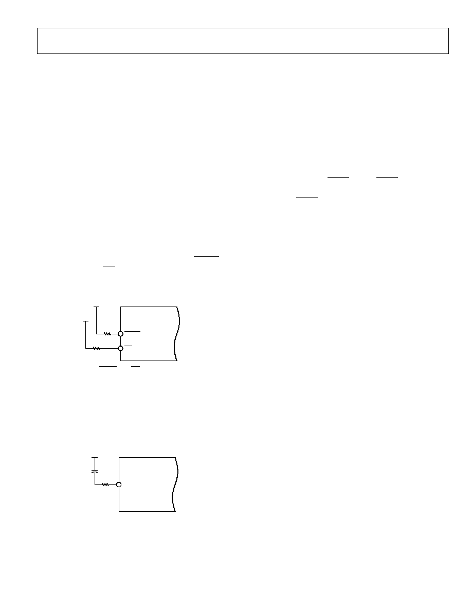
AD6654
Rev. 0 | Page 85 of 88
DDC DESIGN NOTES
The following guidelines describe circuit connections, layout
requirements, and programming procedures for the AD6654.
The designer should review these guidelines before starting the
system design and layout.
· The AD6654 requires the following power-up sequence.
The VDDCORE (1.8 V) is required to settle into nominal
voltage levels before the VDDIO attains the minimum.
· The DDC input clock (CLK) and input (EXP) pins EXP[2:0]
are not 5 V tolerant. Care should be taken to drive these
pins within the limits of VDDIO (3.0 V to 3.6 V). This is
easily accomplished by using the ADC data ready (DR)
output to drive the DDC clock (CLK) input.
· The number format used in this part is twos complement.
All input ports and output ports use twos complement data
format. The formats for individual internal registers are
given in the memory map description of these registers.
· In both microport and serial port operation, the DTACK
(RDY, SDO) and IRP pins are open-drain outputs and
should be terminated externally to VDDIO through a 1 k
pull-up resistor.
05156-056
DTACK (RDY, SDO)
AD6654
1k
3.3V
1k
3.3V
IRP
Figure 75. DTACK, SDO, IRP Pull-Up Resistor Circuit
· A simple RC circuit is used on the EXT_FILTER pin to
balance the internal RC circuit on this pin and maintain a
good PLL clock lock. The recommended circuit is given in
Figure 76. It is further recommended that this RC circuit be
placed as close as possible to the AD6654 part. This layout
consideration ensures that the PLL clock is clean and the
PLL lock is closely maintained.
05156-057
EXT_FILTER
AD6654
250
VDD CORE
0.01
µF
Figure 76. EXT_FILTER Circuit for PLL Clock
· By default, the PLL CLK is disabled. It can be enabled by
programming the PLL multiplier and divider bits in the
ADC CLK control register. When the PLL CLK is enabled
by programming this register, it takes about 50 µs to 200 µs
to settle down. While the PLL loop settles down, the voltage
at the EXT_FILTER pin increases from 0 V to VDDCORE
(1.8 V) and settles there. Channel registers and output port
registers (Address 0x68 to Address 0xE7) should not be pro-
grammed before the PLL loop settles down.
· To reset the AD6654, the user must provide a minimum
pulse of 30 ns to the RESET pin. The RESET pin should be
connected to GND (or pulled low) during power-up of the
part. The RESET pin can be pulled high after the power
supplies have settled to nominal values (1.8 V and
3.3 V). At this point, a pulse (pull low and high again)
should be provided to give a reset to the part.
· The CPUCLK (SCLK) is the clock used for programming
via the microport (serial port). This clock needs to be
provided by the designer to the part (slave clock). The
designer should ensure that this clock's frequency is less
than or equal to the frequency of the CLK signal. Addi-
tionally, the frequency of the CPUCLK (SCLK) should
always be less than 100 MHz.
· The microport data bus is 16 bits wide. Both 8-bit and
16-bit modes are available using this part. If 8-bit mode is
used, the MSB of the data bus (D[15:8]) can be left floating
or connected to GND.
· The output parallel port has a 1-clock cycle overhead. If two
channels (with the same data rates) are output on one
output port in 16-bit interleaved I/Q mode along with an
AGC word, this requires three clock cycles for one sample
from each channel (one clock each for I data, Q data, and
gain data). Therefore, the total number of clock cycles
required to output the data is 3 clocks/channel × 2 channels
+ 1 (overhead) = 7 clock cycles. The number of clock cycles
required for each channel can be 3 (interleaved I + Q + gain
word), or 2 (parallel I /Q + gain) or 2 (interleaved I + Q) or
1 (interleaved I/Q). Designers should make sure that suffi-
cient time is allowed to output these channels on one output
port. Also note that the I, Q, and gain for a particular
channel come out on a single output port and cannot be
divided among output ports.
· When CRCF and DRCF filters are disabled, the coefficient
memory cannot be read back, because the clock to the
coefficient RAM is also cut off.

AD6654
Rev. 0 | Page 86 of 88
· In the Intel mode microport, the beginning of a read and
write access is indicated by the RDY pin going low. The
access is complete only when the RDY pin goes high. In the
Motorola mode microport, the completion of a read and
write access is indicated by the DTACK pin going low. In
both modes, CS, RD (DS), and WR (R/W) should be active
until access is complete; otherwise, an incomplete access
results.
· In both Intel and Motorola modes, if CS is held low even
after microport read or write access is complete, the
microport initiates a second access. This is a problem while
writing or reading from coefficient RAM, where each access
writes to or reads from a different RAM address. This can
be fixed by writing to one coefficient RAM address at a
time, that is, the coefficient start and stop address registers
have the same value.
· In SPI mode programming, the SCS pin must go high
(inactive) after writing or reading each byte (eight clock
cycles on the SCLK pin).
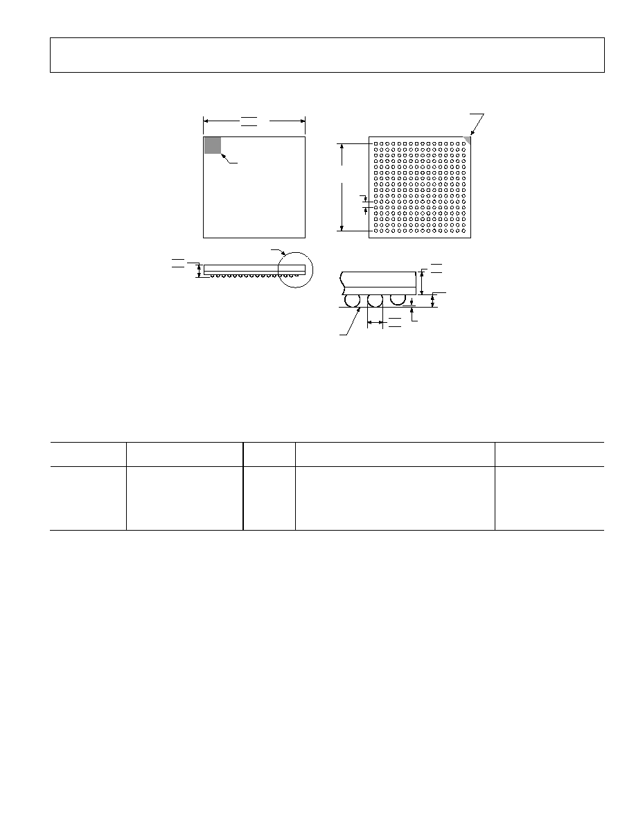
AD6654
Rev. 0 | Page 87 of 88
OUTLINE DIMENSIONS
COMPLIANT TO JEDEC STANDARDS MO-192-AAF-1
EXCEPT FOR DIMENSIONS INDICATED BY A "*" SYMBOL.
1.00
BSC
A
B
C
D
E
F
G
H
J
K
L
M
N
P
R
15
14
13
12
11
10
9
8
7
6
5
4
3
2
1
BOTTOM VIEW
15.00
BSC SQ
A1 CORNER
INDEX AREA
16
T
*1.31
1.21
1.10
COPLANARITY
0.20
0.70
0.60
0.50
BALL DIAMETER
*0.30 MIN
DETAIL A
TOP VIEW
DETAIL A
*1.85
1.71
1.40
17.20
17.00 SQ
16.80
BALL A1
CORNER
SEATING
PLANE
Figure 77. 256-Lead Chip Scale Package Ball Grid Array [CSPBGA]
(BC-256-2)
Dimensions shown in millimeters
ORDERING GUIDE
Model Temperature
Range
Active
Channels
Package Description
Package Option
AD6654BBC
-25°C to +85°C
6
256-Lead CSPBGA (Ball Grid Array)
BC-256-2
AD6654BBCZ
1
-25°C to +85°C
6
256-Lead CSPBGA (Ball Grid Array)
BC-256-2
AD6654CBC
-25°C to +85°C
4
256-Lead CSPBGA (Ball Grid Array)
BC-256-2
AD6654CBCZ
1
-25°C to +85°C
4
256-Lead CSPBGA (Ball Grid Array)
BC-256-2
AD6654/PCB
6
Evaluation Board with AD6654 and Software
1
Z = Pb-free part.

AD6654
Rev. 0 | Page 88 of 88
NOTES
©2005 Analog Devices, Inc. All rights reserved. Trademarks and
registered trademarks are the property of their respective owners.
D0515604/05(0)
Document Outline