 | ÐлекÑÑоннÑй компоненÑ: AD698AP | СкаÑаÑÑ:  PDF PDF  ZIP ZIP |
Äîêóìåíòàöèÿ è îïèñàíèÿ www.docs.chipfind.ru
REV. B
Information furnished by Analog Devices is believed to be accurate and
reliable. However, no responsibility is assumed by Analog Devices for its
use, nor for any infringements of patents or other rights of third parties
which may result from its use. No license is granted by implication or
otherwise under any patent or patent rights of Analog Devices.
a
Universal
LVDT Signal Conditioner
AD698
© Analog Devices, Inc., 1995
One Technology Way, P.O. Box 9106, Norwood. MA 02062-9106, U.S.A.
Tel: 617/329-4700
Fax: 617/326-8703
FEATURES
Single Chip Solution, Contains Internal Oscillator and
Voltage Reference
No Adjustments Required
Interfaces to Half-Bridge, 4-Wire LVDT
DC Output Proportional to Position
20 Hz to 20 kHz Frequency Range
Unipolar or Bipolar Output
Will Also Decode AC Bridge Signals
Outstanding Performance
Linearity: 0.05%
Output Voltage: 11 V
Gain Drift: 20 ppm/ C (typ)
Offset Drift: 5 ppm/ C (typ)
PRODUCT DESCRIPTION
The AD698 is a complete, monolithic Linear Variable Differen-
tial Transformer (LVDT) signal conditioning subsystem. It is
used in conjunction with LVDTs to convert transducer mechan-
ical position to a unipolar or bipolar dc voltage with a high de-
gree of accuracy and repeatability. All circuit functions are
included on the chip. With the addition of a few external passive
components to set frequency and gain, the AD698 converts the
raw LVDT output to a scaled dc signal. The device will operate
with half-bridge LVDTs, LVDTs connected in the series op-
posed configuration (4-wire), and RVDTs.
The AD698 contains a low distortion sine wave oscillator to
drive the LVDT primary. Two synchronous demodulation
channels of the AD698 are used to detect primary and second-
ary amplitude. The part divides the output of the secondary by
the amplitude of the primary and multiplies by a scale factor.
This eliminates scale factor errors due to drift in the amplitude
of the primary drive, improving temperature performance and
stability.
The AD698 uses a unique ratiometric architecture to eliminate
several of the disadvantages associated with traditional ap-
proaches to LVDT interfacing. The benefits of this new cir-
cuit are: no adjustments are necessary; temperature stability is
improved; and transducer interchangeability is improved.
The AD698 is available in two performance grades:
Grade
Temperature Range
Package
AD698AP
40
°
C to +85
°
C
28-Pin PLCC
AD698SQ
55
°
C to +125
°
C
24-Pin Cerdip
PRODUCT HIGHLIGHTS
1. The AD698 offers a single chip solution to LVDT signal
conditioning problems. All active circuits are on the mono-
lithic chip with only passive components required to com-
plete the conversion from mechanical position to dc voltage.
2. The AD698 can be used with many different types of posi-
tion sensors. The circuit is optimized for use with any
LVDT, including half-bridge and series opposed, (4 wire)
configurations. The AD698 accommodates a wide range of
input and output voltages and frequencies.
3. The 20 Hz to 20 kHz excitation frequency is determined by a
single external capacitor. The AD698 provides up to 24 volts
rms to differentially drive the LVDT primary, and the
AD698 meets its specifications with input levels as low as
100 millivolts rms.
4. Changes in oscillator amplitude with temperature will not af-
fect overall circuit performance. The AD698 computes the
ratio of the secondary voltage to the primary voltage to deter-
mine position and direction. No adjustments are required.
5. Multiple LVDTs can be driven by a single AD698 either in
series or parallel as long as power dissipation limits are not
exceeded. The excitation output is thermally protected.
6. The AD698 may be used as a loop integrator in the design of
simple electromechanical servo loops.
7. The sum of the transducer secondary voltages do not need to
be constant.
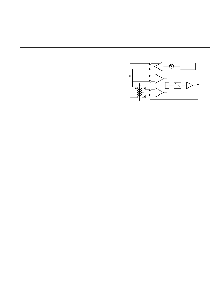
FUNCTIONAL BLOCK DIAGRAM
A
B
AMP
OSCILLATOR
VOLTAGE
REFERENCE
A
B
FILTER
AMP
AD698

AD698SPECIFICATIONS
REV. B
2
(@ T
A
= +25 C, V
CM
= 0 V, and V+, V = 15 V dc, unless otherwise noted)
AD698SQ
AD698AP
Parameter
Min
Typ
Max
Min
Typ
Max
Unit
TRANSFER FUNCTION
1
V
OUT
=
A
B
×
500
µ
A
×
R2
V
OVERALL ERROR T
MIN
to T
MAX
0.4
1.65
0.4
1.65
% of FS
SIGNAL OUTPUT CHARACTERISTICS
Output Voltage Range
11
11
V
Output Current, T
MIN
to T
MAX
11
11
mA
Short Circuit Current
20
20
mA
Nonlinearity
2
T
MIN
to T
MAX
75
500
75
500
ppm of FS
Gain Error
3
0.1
1.0
0.1
1.0
% of FS
Gain Drift
20
100
20
100
ppm/
°
C of FS
Output Offset
0.02
1
0.02
1
% of FS
Offset Drift
5
25
5
25
ppm/
°
C of FS
Excitation Voltage Rejection
4
100
100
ppm/dB
Power Supply Rejection (
±
12 V to
±
18 V)
PSRR Gain
50
300
50
300
ppm/V
PSRR Offset
15
100
15
100
ppm/V
Common-Mode Rejection (
±
3 V)
CMRR Gain
25
100
25
100
ppm/V
CMRR Offset
2
100
2
100
ppm/V
Output Ripple
5
4
4
mV rms
EXCITATION OUTPUT CHARACTERISTICS (@ 2.5 kHz)
Excitation Voltage Range
2.1
24
2.1
24
V rms
Excitation Voltage (Resistors Are 1% Absolute Values)
(R1 = Open)
6
1.2
2.15
1.2
2.15
V rms
(R1 = 12.7 k
)
2.6
4.35
2.6
4.35
V rms
(R1 = 487
)
14
21.2
14
21.2
V rms
Excitation Voltage TC
7
100
100
ppm/
°
C
Output Current
30
50
30
50
mA rms
T
MIN
to T
MAX
40
40
mA rms
Short Circuit Current
60
60
mA
DC Offset Voltage (Differential, R1 = 12.7 k
)
T
MIN
to T
MAX
30
100
30
100
mV
Frequency
20
20 k
20
20 k
Hz
Frequency TC
200
200
ppm/
°
C
Total Harmonic Distortion
50
50
dB
SIGNAL INPUT CHARACTERISTICS
A/B Ratio Usable Full-Scale Range
0.1
0.9
0.l
0.9
Signal Voltage B Channel
0.1
3.5
0.1
3.5
V rms
Signal Voltage A Channel
0.0
3.5
0.0
3.5
V rms
Input Impedance
200
200
k
Input Bias Current (BIN, AIN)
1
5
1
5
µ
A
Signal Reference Bias Current
2
10
2
10
µ
A
Excitation Frequency
0
20 k
0
20 k
Hz
POWER SUPPLY REQUIREMENTS
Operating Range
13
36
13
36
V
Dual Supply Operation (
±
10 V Output)
±
13
±
13
V
Single Supply Operation
0 V to +10 V Output
17.5
17.5
V
0 V to 10 V Output
17.5
17.5
V
Current (No Load at Signal and Excitation Outputs)
12
15
12
15
mA
T
MIN
to T
MAX
18
18
mA
OPERATING TEMPERATURE RANGE
55
+125
40
+85
°
C
AD698
REV. B
3
NOTES
1
A and B represent the Mean Average Deviation (MAD) of the detected sine waves V
A
and V
B
. The polarity of V
OUT
is affected by the sign of the A comparator, i.e.,
multiply V
OUT
×
+1 for A
COMP+
> A
COMP
, and V
OUT
×
1 for A
COMP
> A
COMP+
.
2
Nonlinearity of the AD698 only in units of ppm of full scale. Nonlinearity is defined as the maximum measured deviation of the AD698 output voltage from a
straight line. The straight line is determined by connecting the maximum produced full-scale negative voltage with the maximum produced full-scale positive voltage.
3
See Transfer Function.
4
For example, if the excitation to the primary changes by 1 dB, the gain of the system will change by typically 100 ppm.
5
Output ripple is a function of the AD698 bandwidth determined by C1 and C2. A 1000 pF capacitor should be connected in parallel with R2 to reduce the output
ripple. See Figures 7, 8 and 13.
6
R1 is shown in Figures 7, 8 and 13.
7
Excitation voltage drift is not an important specification because of the ratiometric operation of the AD698.
8
From T
MIN
to T
MAX
the overall error due to the AD698 alone is determined by combining gain error, gain drift and offset drift. For example, the typical overall
error for the AD698AP from T
MIN
to T
MAX
is calculated as follows: Overall Error = Gain Error at +25
°
C (
±
0.2% Full Scale) + Gain Drift from 40
°
C to +25
°
C
(20 ppm/
°
C
×
65
°
C) + Offset Drift from 40
°
C to +25
°
C (5 ppm/
°
C
×
65
°
C) =
±
0.36% of full scale. Note that 1000 ppm of full scale equals 0.1% of full scale.
Specifications subject to change without notice.
Specifications shown in boldface are tested on all production units at final electrical test. Results from those tested are used to calculate outgoing quality levels.
All min and max specifications are guaranteed, although only those shown in boldface are tested on all production units.
ORDERING GUIDE
Model
Package Description
Package Option
AD698AP
28-Pin PLCC
P-28A
AD698SQ
24-Pin Double Cerdip
Q-24A
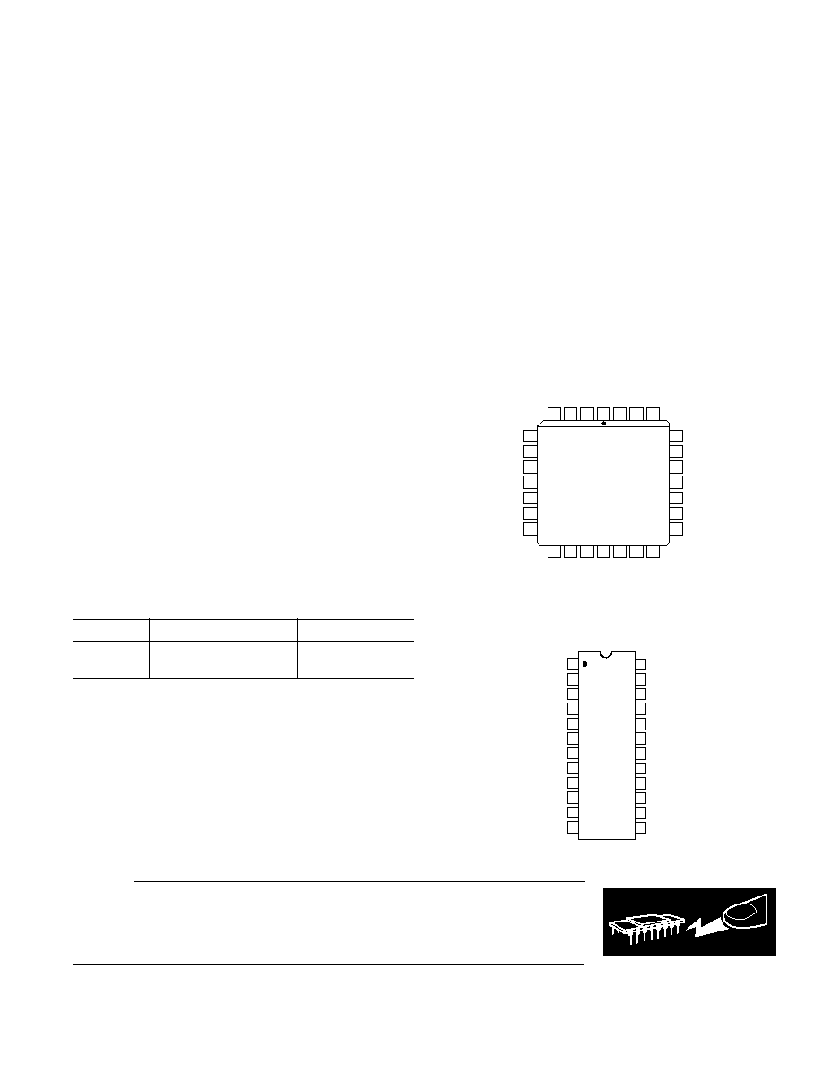
CONNECTION DIAGRAMS
28-Pin PLCC
7
8
9
10
11
5
6
28
27
26
1
2
3
4
21
22
23
24
25
19
20
12 13
14 15
16 17
18
TOP VIEW
(Not to Scale)
LEV1
LEV2
FREQ1
NC
NC
SIG REF
SIG OUT
FEEDBACK
OUT FILT
NC = NO CONNECT
AD698
BFILT1
BFILT2
AFILT1
AFILT2
+ACOMP
FREQ2
NC
EXC2
EXC1
V
S
+V
S
NC
BIN
+BIN
AIN
+AIN
ACOMP
OFF1
OFF2
24-Pin Cerdip
13
16
15
14
24
23
22
21
20
19
18
17
TOP VIEW
(Not to Scale)
12
11
10
9
8
1
2
3
4
7
6
5
AD698
V
S
SIG REF
OFFSET2
OFFSET1
+V
S
EXC1
EXC2
LEV1
OUT FILT
FEEDBACK
SIG OUT
LEV2
FREQ1
FREQ2
BFILT1
BFILT2
BIN
ACOMP
AFILT2
AFILT1
+BIN
AIN
+ACOMP
+AIN
WARNING!
ESD SENSITIVE DEVICE
CAUTION
ESD (electrostatic discharge) sensitive device. Electrostatic charges as high as 4000 V readily
accumulate on the human body and test equipment and can discharge without detection.
Although the AD698 features proprietary ESD protection circuitry, permanent damage may
occur on devices subjected to high energy electrostatic discharges. Therefore, proper ESD
precautions are recommended to avoid performance degradation or loss of functionality.
ABSOLUTE MAXIMUM RATINGS
Total Supply Voltage (+V
S
to V
S
) . . . . . . . . . . . . . . . . . 36 V
Storage Temperature Range
P Package . . . . . . . . . . . . . . . . . . . . . . . . . 65
°
C to +150
°
C
Q Package . . . . . . . . . . . . . . . . . . . . . . . . 65
°
C to +150
°
C
Operating Temperature Range
AD698SQ . . . . . . . . . . . . . . . . . . . . . . . . 55
°
C to +125
°
C
AD698AP . . . . . . . . . . . . . . . . . . . . . . . . . 40
°
C to +85
°
C
Lead Temperature Range (Soldering 60 sec) . . . . . . . . +300
°
C
Power Dissipation Derates above +65
°
C
P Package . . . . . . . . . . . . . . . . . . . . . . . . . . . . . . . 12 mW/
°
C
Q Package . . . . . . . . . . . . . . . . . . . . . . . . . . . . . . 12 mW/
°
C
THERMAL CHARACTERISTICS
JC
JA
P Package 30
°
C/W
60
°
C/W
Q Package 26
°
C/W
62
°
C/W
REV. B
4
AD698
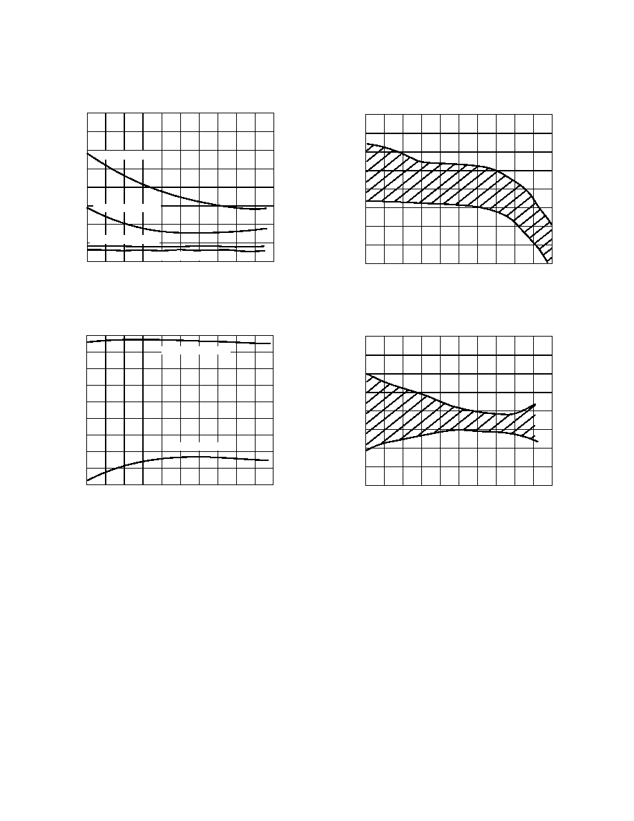
Typical Characteristics
(at +25
°
C and V
S
=
±
15 V unless otherwise noted)
240
20
140
20
0
40
60
80
40
120
160
200
120
100
80
60
40
20
0
20
TEMPERATURE
°
C
GAIN AND OFFSET PSRR ppm/V
OFFSET PSRR 1215V
OFFSET PSRR 1518V
GAIN PSRR 1215V
GAIN PSRR 1518V
Figure 1. Gain and Offset PSRR vs. Temperature
140
40
60
120
100
80
60
40
20
0
20
0
45
35
40
30
25
20
15
10
05
TEMPERATURE
°
C
GAIN AND OFFSET CMRR ppm/V
OFFSET CMRR
±
3V
GAIN CMRR
±
3V
Figure 2. Gain and Offset CMRR vs. Temperature
120
80
140
40
60
40
60
0
20
20
40
80
120
100
80
60
40
20
0
20
TEMPERATURE
°
C
TYPICAL GAIN DRIFT ppm/
°
C
Figure 3. Typical Gain Drift vs. Temperature
20
20
140
10
15
40
60
0
5
5
10
15
120
100
80
60
40
20
0
20
TEMPERATURE
°
C
TYPICAL OFFSET DRIFT ppm/
°
C
Figure 4. Typical Offset Drift vs. Temperature
AD698
REV. B
5
THEORY OF OPERATION
A block diagram of the AD698 along with an LVDT (linear
variable differential transformer) connected to its input is shown
in Figure 5 below. The LVDT is an electromechanical trans-
ducer--its input is the mechanical displacement of a core, and
its output is an ac voltage proportional to core position. Two
popular types of LVDTs are the half-bridge type and the series
opposed or four-wire LVDT. In both types the moveable core
couples flux between the windings. The series-opposed con-
nected LVDT transducer consists of a primary winding ener-
gized by an external sine wave reference source and two
second
ary windings connected in the series opposed configuration.
The output voltage across the series secondary increases as the core
is moved from the center. The direction of movement is detected
by measuring the phase of the output. Half-bridge LVDTs have a
single coil with a center tap and work like an autotransformer. The
excitation voltage is applied across the coil; the voltage at the center
tap is proportional to position. The device behaves similarly to a
resistive voltage divider.
A
B
AMP
OSCILLATOR
VOLTAGE
REFERENCE
A
B
FILTER
AMP
AD698
Figure 5. Functional Block Diagram
The AD698 energizes the LVDT coil, senses the LVDT output
voltages and produces a dc output voltage proportional to core
position. The AD698 has a sine wave oscillator and power am-
plifier to drive the LVDT. Two synchronous demodulation
stages are available for decoding the primary and secondary
voltages. A decoder determines the ratio of the output signal
voltage to the input drive voltage (A/B). A filter stage and out-
put amplifier are used to scale the resulting output.
The oscillator comprises a multivibrator that produces a triwave
output. The triwave drives a sine shaper that produces a low dis-
tortion sine wave. Frequency and amplitude are determined by a
single resistor and capacitor. Output frequency can range from
20 Hz to 20 kHz and amplitude from 2 V to 24 V rms. Total har-
monic distortion is typically 50 dB.
The AD698 decodes LVDTs by synchronously demodulating
the amplitude modulated input (secondaries), A, and a fixed in-
put reference (primary or sum of secondaries or fixed input), B.
A common problem with earlier solutions was that any drift in
the amplitude of the drive oscillator corresponded directly to a
gain error in the output. The AD698, eliminates
these errors by
calculating the ratio of the LVDT output to its input excitation in
order to cancel out any drift effects. This device differs from the
AD598 LVDT signal conditioner in that it implements a different
circuit transfer function and does not require the sum of the LVDT
secondaries (A + B) to be constant with stroke length.
The AD698 block diagram is shown below. The inputs consist
of two independent synchronous demodulation channels. The B
channel is designed to monitor the drive excitation to the LVDT.
The full wave rectified output is filtered by C2 and sent to the
computational circuit. Channel A is identical except that the
comparator is pinned out separately. Since the A channel may
reach 0 V output at LVDT null, the A channel demodulator is
usually triggered by the primary voltage (B Channel). In addi-
tion, a phase compensation network may be required to add a
phase lead or lag to the A Channel to compensate for the LVDT
primary to secondary phase shift. For half-bridge circuits the
phase shift is noncritical, and the A channel voltage is large
enough to trigger the demodulator.
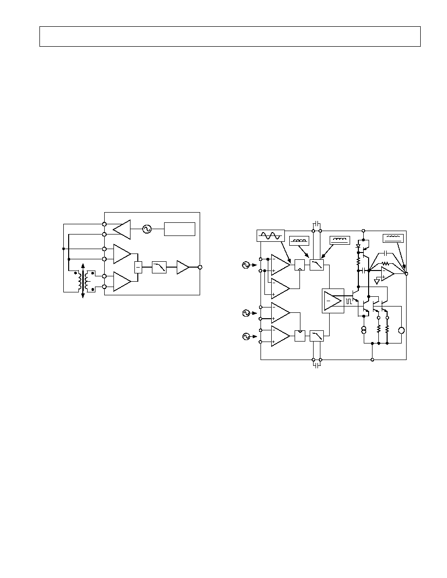
AD698
COMP
±
1
FILTER
B
CHANNEL
BIN
+BIN
DUTY CYCLE
DIVIDER
A/B = 1 = 100%
DUTY
±
1
ACOMP
+ACOMP
AIN
+AIN
FILTER
DEMODULATOR
A
CHANNEL
A
B
OFF 2
OFF 1
BFILT1
BFILT2
C2
V
OUT
IREF
500µA
V
OUT
FILTER
C4
FB
R2
C5
+V
S
V
S
AFILT2
AFILT1
C3
V/I
COMP
V/I
Figure 6. AD698 Block Diagram
Once both channels are demodulated and filtered a division cir-
cuit, implemented with a duty cycle multiplier, is used to calcu-
late the ratio A/B. The output of the divider is a duty cycle.
When A/B is equal to 1, the duty cycle will be equal to 100%.
(This signal can be used as is if a pulse width modulated output
is required.) The duty cycle drives a circuit that modulates and
filters a reference current proportional to the duty cycle. The
output amplifier scales the 500
µ
A reference current converting
it to a voltage. The output transfer function is thus:
V
OUT
=
I
REF
×
A/B
×
R2, where I
REF
=
500
µ
A
REV. B
6
AD698
CONNECTING THE AD698
The AD698 can easily be connected for dual or single supply
operation as shown in Figures 7, 8 and 13. The following gen-
eral design procedures demonstrate how external component
values are selected and can be used for any LVDT that meets
AD698 input/output criteria. The connections for the A and B
channels and the A channel comparators will depend on which
transducer is used. In general follow the guidelines below.
Parameters set with external passive components include: exci-
tation frequency and amplitude, AD698 input signal frequency,
and the scale factor (V/inch). Additionally, there are optional
features; offset null adjustment, filtering, and signal integration,
which can be implemented by adding external components.
R1
C1
15nF
C2
C3
R4
R3
13
16
15
14
24
23
22
21
20
19
18
17
12
11
10
9
8
1
2
3
4
7
6
5
AD698
V
S
EXC1
EXC2
LEV1
LEV2
FREQ1
BFILT1
BFILT2
BIN
+BIN
AIN
FREQ2
SIG REF
OFFSET2
OFFSET1
+V
S
OUT FILT
FEEDBACK
SIG OUT
ACOMP
AFILT2
AFILT1
+ACOMP
+AIN
C4
R2
33k
1000pF
SIGNAL
REFERENCE
R
L
V
OUT
100nF
6.8µF
15V
+15V
100nF
6.8µF
Figure 7. Interconnection Diagram for Half-Bridge LVDT
and Dual Supply Operation
DESIGN PROCEDURE
DUAL SUPPLY OPERATION
Figure 7 shows the connection method for half-bridge LVDTs.
Figure 8 demonstrates the connections for 3- and 4-wire
LVDTs connected in the series opposed configuration. Both ex-
amples use dual
±
15 volt power supplies.
A. Determine the Oscillator Frequency
Frequency is often determined by the required BW of the sys-
tem. However, in some systems the frequency is set to match
the LVDT zero phase frequency as recommended by the
manufacturer; in this case skip to Step 4.
1. Determine the mechanical bandwidth required for LVDT
position measurement subsystem, f
SUBSYSTEM
. For this ex-
ample, assume f
SUBSYSTEM
= 250 Hz.
2. Select minimum LVDT excitation frequency approximately
10
×
f
SUBSYSTEM
. Therefore, let excitation frequency = 2.5 kHz.
3. Select a suitable LVDT that will operate with an excitation
frequency of 2.5 kHz. The Schaevitz E100, for instance, will
operate over a range of 50 Hz to 10 kHz and is an eligible
candidate for this example.
4. Select excitation frequency determining component C1.
C1
=
35
µ
F Hz/f
EXCITATION
R1
C1
C2
C3
R4
R3
13
16
15
14
24
23
22
21
20
19
18
17
12
11
10
9
8
1
2
3
4
7
6
5
AD698
V
S
EXC1
EXC2
LEV1
LEV2
FREQ1
BFILT1
BFILT2
BIN
+BIN
AIN
FREQ2
SIG REF
OFFSET2
OFFSET1
+V
S
OUT FILT
FEEDBACK
SIG OUT
ACOMP
AFILT2
AFILT1
+ACOMP
+AIN
C4
R2
1000pF
SIGNAL
REFERENCE
R
L
V
OUT
100nF
6.8µF
15V
+15V
100nF
6.8µF
1M
A
B
C
D
PHASE
LAG/LEAD
NETWORK
R
T
A
B
C
D
PHASE LEAD
R
S
C
C
R
S
R
S
R
T
A
B
C
D
PHASE LAG
C
PHASE LAG = Arc Tan (Hz RC);
PHASE LEAD = Arc Tan 1/(Hz RC)
WHERE R = R
S
// (R
S
+ R
T
)
Figure 8. AD698 Interconnection Diagram for Series
Opposed LVDT and Dual Supply Operation
B. Determine the Oscillator Amplitude
Amplitude is set such that the primary signal is in the 1.0 V to
3.5 V rms range and the secondary signal is in the 0.25 V to
3.5 V rms range when the LVDT is at its mechanical full-scale
position. This optimizes linearity and minimizes noise suscepti-
bility. Since the part is ratiometric, the exact value of the excita-
tion is relatively unimportant.
5. Determine optimum LVDT excitation voltage, V
EXC
. For a
4-wire LVDT determine the voltage transformation ratio,
VTR, of the LVDT at its mechanical full scale. VTR =
LVDT sensitivity
×
Maximum Stroke Length from null.
LVDT sensitivity is listed in the LVDT manufacturer's cata-
log and has units of volts output per volts input per inch dis-
placement. The E100 has a sensitivity of 2.4 mV/V/mil. In
the event that LVDT sensitivity is not given by the manufac-
turer, it can be computed. See section on determining LVDT
sensitivity.
AD698
REV. B
7
b. Full-scale core displacement from null, d
S
×
d = VTR and also equals the ratio A/B at mechanical full
scale. The VTR should be converted to units of V/V.
For a full-scale displacement of d inches, voltage out of the
AD698 is computed as
V
OUT
= S
×
d
×
500
µ
A
×
R2
V
OUT
is measured with respect to the signal reference,
Pin 21, shown in Figure 7.
Solving for R2,
R2
=
V
OUT
S
×
d
×
500
µ
A
(1)
For V
OUT
=
±
10 V full-scale range (20 V span) and d =
±
0.1
inch full-scale displacement (0.2 inch span)
R2
=
20V
2.4
×
0.2
×
500
µ
A
=
83. 3 k
V
OUT
as a function of displacement for the above example is
shown in Figure 10.
+10
+0.1d (INCHES)
0.1
10
V
OUT
(VOLTS)
Figure 10. V
OUT
(
±
10 V Full Scale) vs. Core Displace-
ment (
±
0.1 Inch)
E. Optional Offset of Output Voltage Swing
9. Selections of R3 and R4 permit a positive or negative output
voltage offset adjustment.
V
OS
=
1.2 V
×
R2
×
1
R3
+
2 k
1
R4
+
2 k
(2)
For no offset adjustment R3 and R4 should be open circuit.
To design a circuit producing a 0 V to +10 V output for a
displacement of +0.1 inch, set V
OUT
to +10 V, d = 0.2 inch
and solve Equation (1) for R2.
+5
+0.1d (INCHES)
0.1
5
V
OUT
(VOLTS)
Figure 11. V
OUT
(
±
5 V Full Scale) vs. Core Displacement
(
±
0.1 Inch)
This will produce a response shown in Figure 11.
In Equation (2) set V
OS
= 5 V and solve for R3 and R4. Since a
positive offset is desired, let R4 be open circuit. Rearranging
Equation (2) and solving for R3
R3
=
1.2
×
R2
V
OS
2 k
=
7.02 k
Multiply the primary excitation voltage by the VTR to get
the expected secondary voltage at mechanical full scale. For
example, for an LVDT with a sensitivity of 2.4 mV/V/mil and
a full scale of
±
0.1 inch, the VTR = 0.0024 V/V/Mil
×
100
mil = 0.24. Assuming the maximum excitation of 3.5 V rms,
the maximum secondary voltage will be 3.5 V rms
×
0.24 =
0.84 V rms, which is in the acceptable range.
Conversely the VTR may be measured explicitly. With the
LVDT energized at its typical drive level V
PRI
, as indicated
by the manufacturer, set the core displacement to its me-
chanical full-scale position and measure the output V
SEC
of
the secondary. Compute the LVDT voltage transformation
ratio, VTR. VTR = V
SEC
//VPRI. For the E100, V
SEC
= 0.72 V
for V
PRI
= 3 V. VTR = 0.24.
For situations where LVDT sensitivity is low, or the me-
chanical FS is a small fraction of the total stroke length, an
input excitation of more than 3.5 V rms may be needed. In
this case a voltage divider network may be placed across the
LVDT primary to provide smaller voltage for the +BIN and
BIN input. If, for example, a network was added to divide
the B Channel input by 1/2, then the VTR should also be re-
duced by 1/2 for the purpose of component selection.
Check the power supply voltages by verifying that the peak
values of V
A
and V
B
are at least 2.5 volts less than the volt-
ages at +V
S
and V
S
.
6. Referring to Figure 9, for V
S
=
±
15 V, select the value of the
amplitude determining component R1 as shown by the curve
in Figure 9.
30
15
0
0.01
0.1
1k
100
10
1
5
10
20
25
V rms
R1 k
V
EXC
V
r
m
s
Figure 9. Excitation Voltage V
EXC
vs. R1
7. C2, C3 and C4 are a function of the desired bandwidth of
the AD698 position measurement subsystem. They should
be nominally equal values.
C2 = C3 = C4 = 10
4
Farad Hz/f
5UBSYSTEM
(Hz)
If the desired system bandwidth is 250 Hz, then
C2 = C3 = C4 = 10
-4
Farad Hz/250 Hz = 0.4
µ
F
See Figures 14, 15 and 16 for more information about
AD698 bandwidth and phase characterization.
D. Set the Full-Scale Output Voltage
8. To compute R2, which sets the AD698 gain or full-scale
output range, several pieces of information are needed:
a. LVDT sensitivity, S
REV. B
8
AD698
Note that V
OS
should
be chosen so that R3 cannot have negative
value .
Figure 12 shows the desired response.
+5
+0.1d (INCHES)
0.1
V
OUT
(VOLTS)
+10
Figure 12. V
OUT
(0 V10 V Full Scale) vs. Displacement
(
±
0.1 Inch)
DESIGN PROCEDURE
SINGLE SUPPLY OPERATION
Figure 13 shows the single supply connection method.
R1
C1
C2
C3
R4
R3
13
16
15
14
24
23
22
21
20
19
18
17
12
11
10
9
8
1
2
3
4
7
6
5
AD698
V
S
EXC1
EXC2
LEV1
LEV2
FREQ1
BFILT1
BFILT2
BIN
+BIN
AIN
FREQ2
SIG REF
OFFSET2
OFFSET1
+V
S
OUT FILT
FEEDBACK
SIG OUT
ACOMP
AFILT2
AFILT1
+ACOMP
+AIN
C4
R2
1000pF
SIGNAL
REFERENCE
R
L
V
OUT
0.1µF
V
ps
+30V
6.8µF
1M
R6
R5
C5
A
B
C
D
PHASE
LAG/LEAD
NETWORK
R
T
A
B
C
D
PHASE LEAD
R
S
C
C
R
S
R
S
R
T
A
B
C
D
PHASE LAG
C
PHASE LAG = Arc Tan (Hz RC);
PHASE LEAD = Arc Tan 1/(Hz RC)
WHERE R = R
S
// (R
S
+ R
T
)
Figure 13. Interconnection Diagram for Single Supply
Operation
For single supply operation, repeat Steps 1 through 10 of the
design procedure for dual supply operation. R5, R6 and C5 are
additional component values to be determined. V
OUT
is mea-
sured with respect to SIGNAL REFERENCE.
10. Compute a maximum value of R5 and R6 based upon the
relationship
R5 + R6
V
PS
/100
µ
A
11. The voltage drop across R5 must be greater than
2
+
10 k
1.2V
R4
+
2 k
+
250
µ
A
+
V
OUT
4
×
R2
Volts
Therefore
R5
2
+
10 k
1.2V
R4
+
2 k
+
250
µ
A
+
V
OUT
4
×
R2
100
µ
A
Ohms
Based upon the constraints of R5 + R6 (Step 10) and R5 (Step
11), select an interim value of R6.
12. Load current through R
L
returns to the junction of R5 and
R6, and flows back to V
PS
. Under maximum load condi-
tions, make sure the voltage drop across R5 is met as de-
fined in Step 11.
As a final check on the power supply voltages, verify that
the peak values of V
A
and V
B
are at least 2.5 volts less than
the voltage between +V
S
and V
S
.
13. C5 is a bypass capacitor in the range of 0.1
µ
F to 1
µ
F.
Gain Phase Characteristics
To use an LVDT in a closed-loop mechanical servo application,
it is necessary to know the dynamic characteristics of the trans-
ducer and interface elements. The transducer itself is very quick
to respond once the core is moved. The dynamics arise prima-
rily from the interface electronics. Figures 14, 15 and 16 show
the frequency response of the AD698 LVDT Signal Conditioner.
Note that Figures 15 and 16 are basically the same; the differ-
ence is frequency range covered. Figure 15 shows a wider range
of mechanical input frequencies at the expense of accuracy.
FREQUENCY Hz
0
10k
100
1k
10
0
30
60
70
0
10
20
50
40
GAIN dB
360
60
240
300
420
180
120
PHASE SHIFT Degrees
0.1µF
0.33µF
2.0µF
R2 = 81k
f
EXC
= 2.5kHz
0.1µF
0.33µF
2.0µF
R2 = 81k
f
EXC
= 2.5kHz
Figure 14. Gain and Phase Characteristics vs. Frequency
(0 kHz10 kHz)
AD698
REV. B
9
FREQUENCY Hz
0
100k
100
1k
10k
10
0
30
60
70
0
10
20
50
40
360
60
240
300
420
180
120
GAIN dB
PHASE SHIFT Degrees
0.1µF
0.033µF
0.01µF
R2 = 81k
f
EXC
= 10kHz
0.1µF
0.033µF
0.01µF
R2 = 81k
f
EXC
= 10kHz
Figure 15. Gain and Phase Characteristics vs. Frequency
(0 kHz50 kHz)
FREQUENCY Hz
0
100
1k
10k
10
0
30
60
70
10
20
50
40
0
360
60
240
300
180
120
GAIN dB
PHASE SHIFT Degrees
0.1µF
0.033µF
0.01µF
R2 = 81k
f
EXC
= 10kHz
0.1µF
0.033µF
0.01µF
R2 = 81k
f
EXC
= 10kHz
Figure 16. Gain and Phase Characteristics vs. Frequency
(0 kHz10 kHz)
Figure 16 shows a more limited frequency range with enhanced
accuracy. The figures are transfer functions with the input to be
considered as a sinusoidally varying mechanical position and the
output as the voltage from the AD698; the units of the transfer
function are volts per inch. The value of C2, C3, and C4, from
Figure 7, are all equal and designated as a parameter in the fig-
ures. The response is approximately that of two real poles.
However, there is appreciable excess phase at higher frequen-
cies. An additional pole of filtering can be introduced with a
shunt capacitor across R2, Figure 7; this will also increase phase
lag.
When selecting values of C2, C3 and C4 to set the bandwidth of
the system, a trade-off is involved. There is ripple on the "dc"
position output voltage, and the magnitude is determined by the
filter capacitors. Generally, smaller capacitors will give higher
system bandwidth and larger ripple. Figures 17 and 18 show the
magnitude of ripple as a function of C2, C3 and C4, again all
equal in value. Note also a shunt capacitor across R2, Figure 7,
is shown as a parameter. The value of R2 used was 81 k
with a
Schaevitz E100 LVDT.
C2, C3, C4; C2 = C3 = C4
µ
F
RIPPLE mV rms
1k
100
0.1
0.01
0.1
10
1
10
1
2.5kHz, C
SHUNT
1nF
2.5kHz, C
SHUNT
10nF
Figure 17. Output Voltage Ripple vs. Filter Capacitance
C2, C3, C4; C2 = C3 = C4
µ
F
RIPPLE mV rms
1k
100
0.1
0.001
0.01
10
0.1
10
1
10kHz, C
SHUNT
1nF
10kHz, C
SHUNT
10nF
1
Figure 18. Output Voltage Ripple vs. Filter Capacitance

REV. B
10
AD698
Determining LVDT Sensitivity
LVDT sensitivity can be determined by measuring the LVDT
secondary voltages as a function of primary drive and core posi-
tion, and performing a simple computation.
Energize the LVDT at its recommended primary drive level,
V
PRI
(3 V rms for the E100). Set the core displacement to its
mechanical full-scale position and measure secondary voltages
V
A
and V
B
.
Sensitivity
=
V
SECONDARY
V
PRI
×
d
From Figure 19,
Sensitivity
=
0.72
3 V
×
100 mils
=
2.4 mV /V mil
d = 100 mils
d = 0
1.71V rms
0.99V rms
d = +100 mils
V
SEC
WHEN V
PRI
3V rms
V
A
V
B
Figure 19. LVDT Secondary Voltage vs. Core
Displacement
Thermal Shutdown and Loading Considerations
The AD698 is protected by a thermal overload circuit. If the die
temperature reaches 165
°
C, the sine wave excitation amplitude
gradually reduces, thereby lowering the internal power dissipa-
tion and temperature.
Due to the ratiometric operation of the decoder circuit, only
small errors result from the reduction of the excitation ampli-
tude. Under these conditions the signal-processing section of
the AD698 continues to meet its output specifications.
The thermal load depends upon the voltage and current deliv-
ered to the load as well as the power supply potentials. An
LVDT Primary will present an inductive load to the sine wave
excitation. The phase angle between the excitation voltage and
current must also be considered, further complicating thermal
calculations.
APPLICATIONS
Most of the applications for the AD598 can also be imple-
mented with the AD698. Please refer to the applications written
for the AD598 for a detailed explanation.
See AD598 data sheet for:
Proving Ring-Weigh Scale
Synchronous Operation of Multiple LVDTs
High Resolution Position-to-Frequency Circuit
Low Cost Setpoint Controller
Mechanical Follower Servo Loop
Differential Gaging and Precision Differential Gaging
AC BRIDGE SIGNAL CONDITIONER
Bridge circuits which use dc excitation are often plagued by er-
rors caused by thermocouple effects, 1/f noise, dc drifts in the
electronics, and line noise pickup. One way to get around these
problems is to excite the bridge with an ac waveform, amplify
the bridge output with an ac amplifier, and synchronously de-
modulate the resulting signal. The ac phase and amplitude in-
formation from the bridge is recovered as a dc signal at the
output of the synchronous demodulator. The low frequency
system noise, dc drifts, and demodulator noise all get mixed to
the carrier frequency and can be removed by means of a low-
pass filter.
The AD698 with the addition of a simple ac gain stage can be
used to implement an ac bridge. Figure 20 shows the connec-
tions for such a system. The AD698 oscillator provides ac
excitation for the bridge. The low level bridge signal is amplified
by the gain stage created by A1, A2 to provide a differential in-
put to the A Channel of the AD698. The signal is then synchro-
nously detected by A Channel. The B Channel is used to detect
the level of the bridge excitation. The ratio of A/B is then calcu-
lated and converted to an output voltage by R2. An optional
phase lag/lead network can be added in front of the A compara-
tor to adjust for phase delays through the bridge and the ampli-
fier, or if the phase delay is small, it can be ignored or compensated
for by a gain adjustment.
This circuit can be used for resistive bridges such as strain
gages, or for inductive or capacitive bridges that are commonly
used for pressure or flow sensors. The low level signal outputs of
these sensors are susceptible to noise and interference and are
good candidates for ac signal processing techniques.
Component Selection
Amplifiers A1, A2 will be chosen depending on the type of
bridge that is conditioned. Capacitive bridges should use an
amplifier with low bias current; a large bleeder resistor will be
required from the amplifier inputs to ground to provide a path
for the dc bias current. Resistive and inductive bridges can use a
more general purpose amplifier. The dc performance of A1, A2
are not as important as their ac performance. DC errors such as
voltage offset will be chopped out by the AD698 since they are
not synchronous to the carrier frequency.
The oscillator amplitude and span resistor for the AD698 may
be chosen by first computing the transfer function or sensitivity
of the bridge and the ac amplifier. This ratio will correspond to
the A/B term in the AD698 transfer function. For example, sup-
pose that a resistive strain gage with a sensitivity, S, of 2 mV/V
at full scale is used. Select an arbitrary target value for A/B that
is close to its maximum value such as A/B = 0.8. Then choose a
gain for the ac amplifier so that the strain gage transfer function
from excitation to output also equals 0.8. Thus the required am-
plifier gain will be [A/B]/ S; or 0.8/ 0.002 V/V = 400. Then
select values for R
S
and R
G
. For the gain stage:
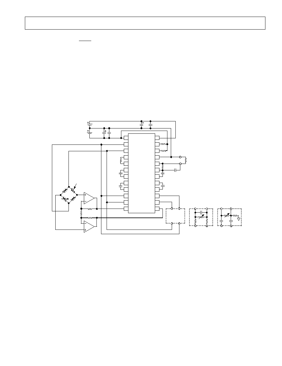
AD698
REV. B
11
V
OUT
=
2
×
R
S
R
G
+
1
×
V
IN
Solving for V
OUT
/V
IN
= 400 and setting R
G
= 100
then:
R
S
= [400 1]
×
R
G
/2 = 19.95 k
Choose an oscillator amplitude that is in the range of 1 V to
3.5 V rms. For an input excitation level of 3 V rms, the output
signal from the amplifier gain stage will be 3.5 V rms
×
0.8 V or
2.4 V rms, which is in the acceptable range.
Since A/B is known, the value of R2, the output FS resistor may
be chosen by the formula:
V
OUT
= A/B
×
500
µ
A
×
R2
For a 10 V output at FS, with an A/B of 0.8; solve for R2.
R2 = 10 V [0.8
×
500
µ
A] = 25.0 k
This will result in a V
OUT
of 10 V for a full-scale signal from the
bridge. The other components, C1, C2, C3, C4 may be selected
by following the guidelines on general device operation men-
tioned earlier.
If a gain trim is required, then a trim resistor can be used to ad-
just either R2 or R
G
. Bridge offsets should be adjusted by a trim
network on the OFFSET 1 and OFFSET 2 pins of the AD698.
R1
C1
C2
C3
R4
R3
C4
R2
1000pF
SIGNAL
REFERENCE
R
L
V
OUT
100nF
6.8µF
15V
+15V
100nF
6.8µF
A
B
C
D
PHASE
LAG/LEAD
NETWORK
13
16
15
14
24
23
22
21
20
19
18
17
12
11
10
9
8
1
2
3
4
7
6
5
AD698
V
S
EXC1
EXC2
LEV1
LEV2
FREQ1
BFILT1
BFILT2
BIN
+BIN
AIN
FREQ2
SIG REF
OFFSET2
OFFSET1
+V
S
OUT FILT
FEEDBACK
SIG OUT
ACOMP
AFILT2
AFILT1
+ACOMP
+AIN
A2
R
S
A1
R
S
RESISTORS,
INDUCTORS
OR CAPACITORS
R
T
A
B
C
D
PHASE LEAD
R
S
C
C
R
S
R
S
R
T
A
B
C
D
PHASE LAG
C
PHASE LAG = Arc Tan (Hz RC);
PHASE LEAD = Arc Tan 1/(Hz RC)
WHERE R = R
S
// (R
S
+ R
T
)
R
G
DUAL
OP AMP
Figure 20. AD698 Interconnection Diagram for AC Bridge Applications
REV. B
12
AD698
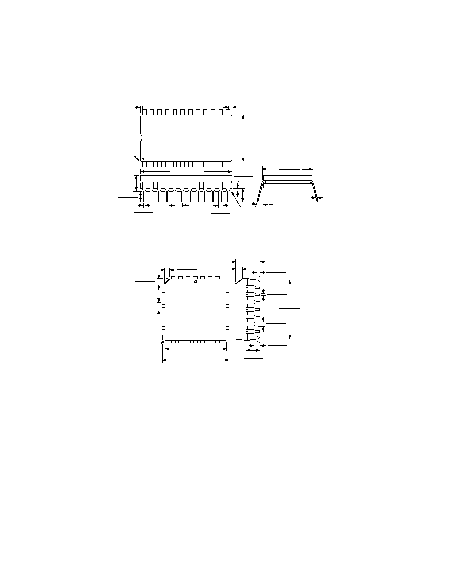
OUTLINE DIMENSIONS
Dimensions shown in inches and (mm).
24-Pin Cerdip (Wide)
0.620 (15.75)
0.590 (15.00)
0.015 (0.38)
0.008 (0.20)
15
°
0
°
1.280 (32.51) MAX
0.200
(5.08)
MAX
0.023 (0.58)
0.014 (0.36)
0.200 (5.08)
0.125 (3.18)
0.100
(2.54)
BSC
0.070 (1.78)
0.030 (0.76)
0.060 (1.52)
0.015 (0.38)
0.150
(3.81)
MIN
SEATING
PLANE
0.005 (0.13) MIN
PIN 1
1
24
0.098 (2.49) MAX
0.610 (15.5)
0.520 (13.2)
12
13
28-Pin PLCC
0.048 (1.21)
0.042 (1.07)
0.456 (11.58)
0.450 (11.43)
SQ
0.495 (12.57)
0.485 (12.32)
SQ
0.048 (1.21)
0.042 (1.07)
0.050
(1.27)
BSC
26
4
TOP VIEW
25
19
12
11
PIN 1
IDENTIFIER
5
18
0.020
(0.50)
R
0.032 (0.81)
0.026 (0.66)
0.021 (0.53)
0.013 (0.33)
0.056 (1.42)
0.042 (1.07)
0.025 (0.63)
0.015 (0.38)
0.180 (4.57)
0.165 (4.19)
0.430 (10.92)
0.390 (9.91)
0.110 (2.79)
0.085 (2.16)
0.040 (1.01)
0.025 (0.64)
C1827a57/95
PRINTED IN U.S.A.