Äîêóìåíòàöèÿ è îïèñàíèÿ www.docs.chipfind.ru
REV. B
Information furnished by Analog Devices is believed to be accurate and
reliable. However, no responsibility is assumed by Analog Devices for its
use, nor for any infringements of patents or other rights of third parties
which may result from its use. No license is granted by implication or
otherwise under any patent or patent rights of Analog Devices.
a
AD7008
© Analog Devices, Inc., 1995
One Technology Way, P.O. Box 9106, Norwood. MA 02062-9106, U.S.A.
Tel: 617/329-4700
Fax: 617/326-8703
CMOS
DDS Modulator
FEATURES
Single +5 V Supply
32-Bit Phase Accumulator
On-Chip COSINE and SINE Look-Up Tables
On-Chip 10-Bit DAC
Frequency, Phase and Amplitude Modulation
Parallel and Serial Loading
Software and Hardware Power Down Options
20 MHz and 50 MHz Speed Grades
44-Pin PLCC
APPLICATIONS
Frequency Synthesizers
Frequency, Phase or Amplitude Modulators
DDS Tuning
Digital Modulation
phase modulation, frequency modulation, and both in-phase and
quadrature amplitude modulation suitable for QAM and SSB
generation.
Clock rates up to 20 MHz and 50 MHz are supported. Fre-
quency accuracy can be controlled to one part in 4 billion.
Modulation may be effected by loading registers either through
the parallel microprocessor interface or the serial interface. A
frequency-select pin permits selection between two frequencies
on a per cycle basis.
The serial and parallel interfaces may be operated independently
and asynchronously from the DDS clock; the transfer control
signals are internally synchronized to prevent metastability prob-
lems. The synchronizer can be bypassed to reduce the transfer
latency in the event that the microprocessor clock is synchro-
nous with the DDS clock.
A power-down pin allows external control of a power-down
mode (also accessible through the microprocessor interface)
The AD7008 is available in 44-pin PLCC.
PRODUCT HIGHLIGHT
1. Low Power
2. DSP/
µ
P Interface
3. Completely Integrated
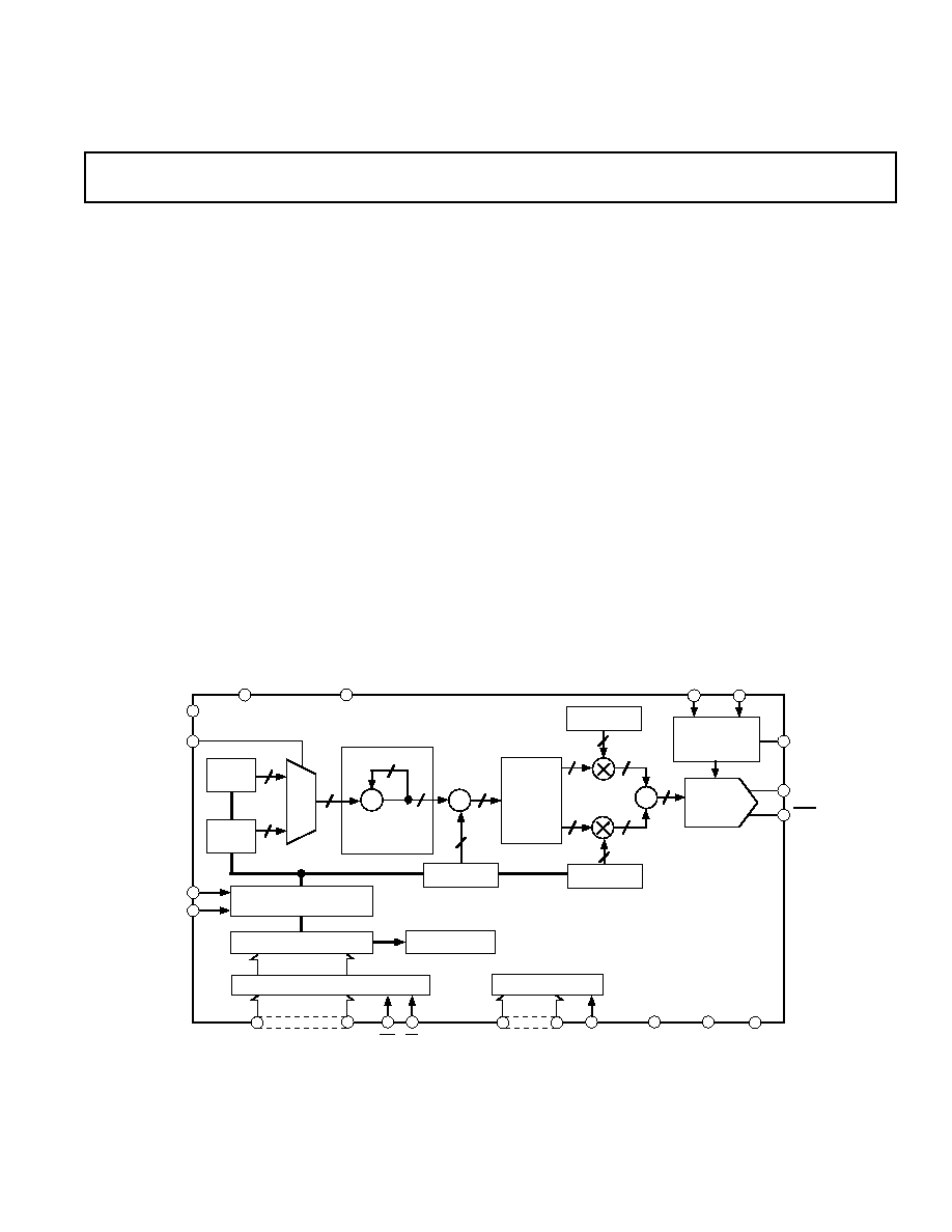
PRODUCT DESCRIPTION
The AD7008 direct digital synthesis chip is a numerically con-
trolled oscillator employing a 32-bit phase accumulator, sine and
cosine look-up tables and a 10-bit D/A converter integrated on a
single CMOS chip. Modulation capabilities are provided for
FUNCTIONAL BLOCK DIAGRAM
32
32
12
10
10
10
10
10
SIN
COS
12
10-BIT DAC
PHASE
ACCUMULATOR
SIN/COS
ROM
IQMOD [9:0]
IOUT
COMP
FS ADJUST
SDATA
SCLK
GND
RESET
TEST
CLOCK
V
AA
WR
CS
IOUT
AD7008
32-BIT SERIAL REGISTER
32-BIT PARALLEL REGISTER
COMMAND REG
MPU INTERFACE
TRANSFER LOGIC
FULLSCALE
ADJUST
10
IQMOD [19:10]
12
PHASE REG
D0
D15
32
32
FSELECT
MUX
FREQ1
REG
TC0
TC3
LOAD
10
FREQ0
REG
SLEEP
V
REF

AD7008SPECIFICATIONS
1
AD7008AP20
AD7008JP50
Test Conditions/
Parameter
Min
Typ
Max
Min
Typ
Max
Units
Comments
SIGNAL DAC SPECIFICATIONS
Resolution
10
10
Bits
Update Rate (f
MAX
)
20
50
MSPS
IOUT Full Scale
20
20
mA
Output Compliance
1
1
Volts
DC Accuracy
Integral Nonlinearity
+1
+1
LSB
Differential Nonlinearity
±
1
±
1
LSB
DDS SPECIFICATIONS
2
Update Rate (f
MAX
)
20
50
MSPS
Dynamic Specifications
Signal-to-Noise
50
50
dB
f
CLK
= f
MAX
,
f
OUT
= 2 MHz
Total Harmonic Distortion
55
53
dB
f
CLK
= f
MAX
,
f
OUT
= 2 MHz
Spurious Free Dynamic Range (SFDR)
3
Narrow Band (
±
50 kHz)
70
70
dBc
f
CLK
= 6.25 MHz,
f
OUT
= 2.11 MHz
Wide Band (
±
2 MHz)
55
55
dBc
VOLTAGE REFERENCE
Internal Reference @ +25
°
C
4
1.2
1.27
1.35
1.2
1.27
1.35
Volts
Reference TC
300
300
ppm/
°
C
V
REF
Overdrive
5
0
2
0
2
V
LOGIC INPUTS
V
INH
, Input High Voltage
V
DD
0.9
V
DD
0.9
Volts
V
INL
, Input Low Voltage
0.9
0.9
Volts
I
INH
, Input Current
10
10
µ
A
C
IN
, Input Capacitance
10
10
pF
POWER SUPPLIES
V
DD
4.75
5.25
4.75
5.25
Volts
I
AA
26
26
mA
R
SET
= 390
I
DD
22 + 1.5/MHz
22 + 1.5/MHz
mA
I
AA
+ I
DD
f
CLK
= Max
80
110
125
160
mA
Sleep = V
DD
10
20
mA
NOTES
1
Operating temperature ranges as follows: A Version: 40
°
C to +85
°
C; J Version: 0
°
C to +70
°
C.
2
All dynamic specifications are measured using IOUT. 100% Production tested.
3
f
CLK
= 6.25 MHz, Frequency Word = 5671C71C HEX, f
OUT
= 2.11 MHz.
4
V
REF
may be externally driven between 0 and V
DD
.
5
Do not allow reference current to cause power dissipation beyond the limit of I
AA
+ I
DD
shown above.
Specifications subject to change without notice.
REV. B
2
(V
AA
= V
DD
= +5 V
±
5%; T
A
= T
MIN
to T
MAX
, R
SET
= 390
, R
LOAD
= 1
for
IOUT and IOUT, unless otherwise noted)
AD7008
REV. B
3
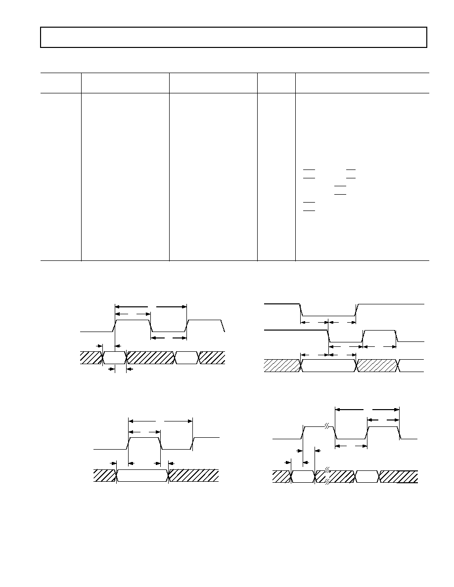
TIMING CHARACTERISTICS
(V
AA
= V
DD
+5 V
±
5%; T
A
= T
MIN
to T
MAX
, unless otherwise noted)
AD7008AP20
AD7008JP50
Parameter
Min
Typ
Max
Min
Typ
Max
Units
Test Conditions/Comments
t
1
50
20
ns
CLOCK Period
t
2
20
8
ns
CLOCK High Duration
t
3
20
8
ns
CLOCK Low Duration
t
4
5
5
ns
CLOCK to Control Setup Time
t
5
3
3
ns
CLOCK to Control Hold Time
t
6
4t
1
4t
1
ns
LOAD Period
t
7
2t
1
2t
1
ns
LOAD High Duration
1
t
8
5
5
ns
LOAD High to TC0TC3 Setup Time
t
9
5
5
ns
LOAD High to TC0TC3 Hold Time
t
10
10
10
ns
WR
Falling to CS Low Setup Time
t
11
10
10
ns
WR
Falling to CS Low Hold Time
t
12
20
20
ns
Minimum WR Low Duration
t
13
10
10
ns
Minimum WR High Duration
t
14
3
3
ns
WR
to D0D15 Setup Time
t
15
3
3
ns
WR
to D0D15 Hold Time
t
16
20
20
ns
SCLK Period
t
17
8
8
ns
SCLK High Duration
t
18
8
8
ns
SCLK Low Duration
t
19
10
10
ns
SCLK Rising to SDATA Setup Time
t
20
10
10
ns
SCLK Rising to SDATA Hold Time
NOTE
1
May be reduced to 1t
1
if LOAD is synchronized to CLOCK and Setup (t
4
) and Hold (t
5
) Times for LOAD to CLOCK are observed.
D0D15
VALID DATA
CS
WR
t
11
t
10
t
12
t
13
t
15
t
14
Figure 3. Parallel Port Timing
SCLK
DB31
SDATA
DB0
t
20
t
16
t
17
t
19
t
18
Figure 4. Serial Port Timing
Figure 2. Register Transfer Timing
LOAD
TC0TC3
VALID
t
9
t
8
t
6
t
7
CLOCK
FSEL, LOAD,
TC3TC0
VALID
VALID
t
1
t
3
t
4
t
5
t
2
Figure 1. Clock Synchronization Timing
REV. B
4
AD7008
ABSOLUTE MAXIMUM RATINGS*
(T
A
= +25
°
C unless otherwise noted)
V
AA
, V
DD
to GND . . . . . . . . . . . . . . . . . . . . . . . 0.3 V to +7 V
AGND to DGND . . . . . . . . . . . . . . . . . . . . . 0.3 V to +0.3 V
Digital I/O Voltage to DGND . . . . . . . . 0.3 V to V
DD
+ 0.3 V
Analog I/O Voltage to AGND . . . . . . . . 0.3 V to V
DD
+ 0.3 V
Operating Temperature Range
Industrial (A Version) . . . . . . . . . . . . . . . . . 40
°
C to +85
°
C
Commercial (J Version) . . . . . . . . . . . . . . . . . . 0
°
C to +70
°
C
Storage Temperature Range . . . . . . . . . . . . . 65
°
C to +150
°
C
Lead Temperature (Soldering, 10 secs) . . . . . . . . . . . . +300
°
C
Junction Temperature . . . . . . . . . . . . . . . . . . . . . . . . . +115
°
C
PLCC
JA
Thermal Impedance . . . . . . . . . . . . . . . +53.8
°
C/W
JC
Thermal Impedance . . . . . . . . . . . . . . . +24.1
°
C/W
*Stresses above those listed under "Absolute Maximum Ratings" may cause
permanent damage to the device. This is a stress rating only and functional
operation of the device at these or any other conditions above those listed in the
operational sections of this specification is not implied. Exposure to absolute
maximum rating conditions for extended periods may affect device reliability.
ORDERING GUIDE
Temperature
Package
Package
Model
Range
Description
Option
AD7008AP20
40
°
C to +85
°
C
44-Pin PLCC P-44A
AD7008JP50
0
°
C to +70
°
C
44-Pin PLCC P-44A
AD7008/PCB*
13.5" Disk
*AD7008/PCB DDS Evaluation Kit, assembled and tested. Kit includes an
AD7008JP50.
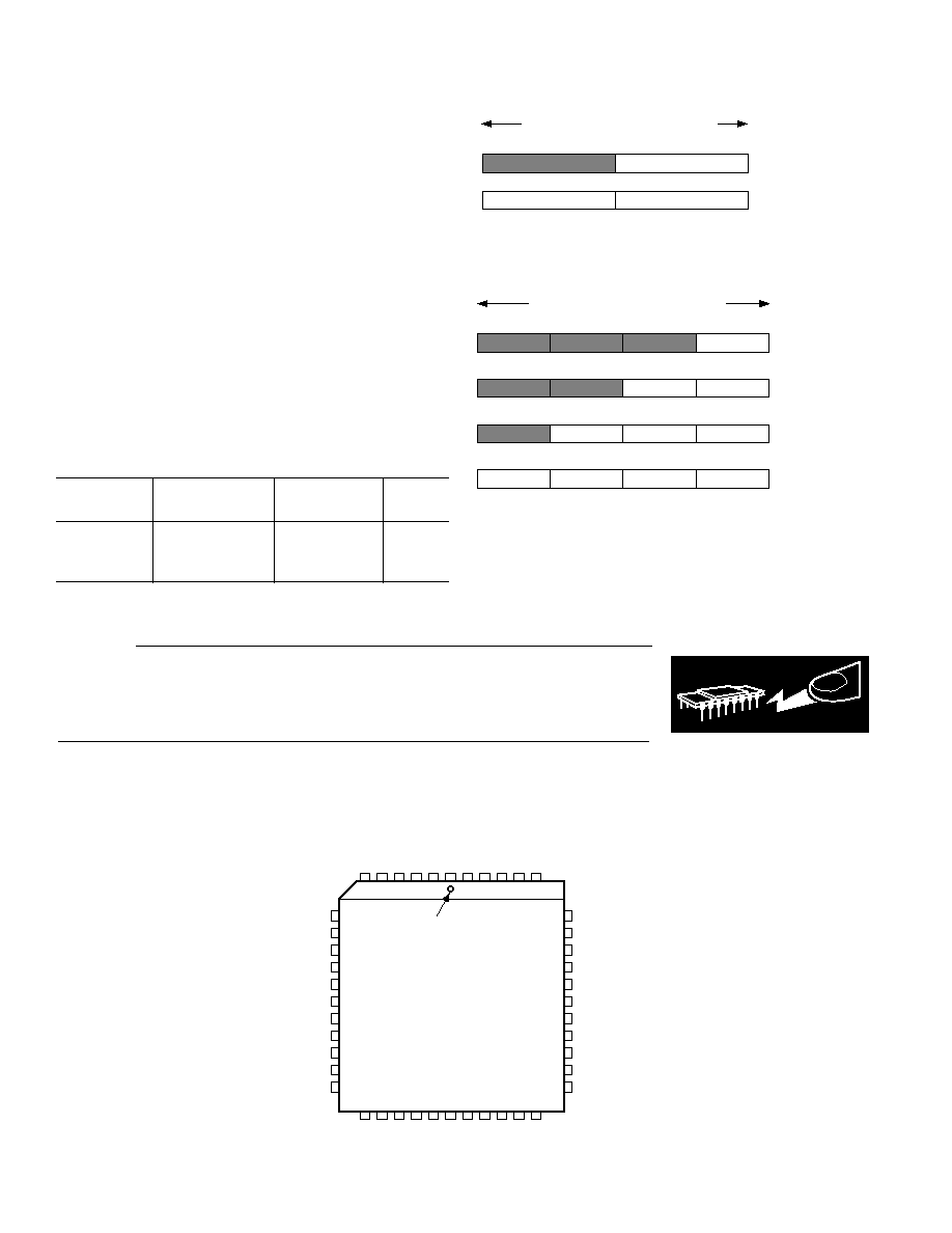
PIN CONFIGURATION
PLCC
PIN NO. 1 IDENTIFIER
6
40
18
28
7
39
17
29
AD7008 PLCC
TOP VIEW
(NOT TO SCALE)
V
DD
RESET
SLEEP
LOAD
TC3
TC2
TC1
TC0
FSELECT
CLOCK
DGND
V
REF
COMP
FS ADJUST
V
AA
IOUT
AGND
DGND
SDATA
SCLK
TEST
IOUT
DGND
D0
D1
D2
D3
D4
D5
D6
D7
V
DD
CS
DGND
D8
D9
D10
D11
D12
D13
D14
D15
V
DD
WR
MSB
LSB
A WORD
D15D0
A WORD*
B WORD
D15D0
B WORD
A WORD
32-BIT PARALLEL ASSEMBLY REGISTER
*MOST SIGNIFICANT WORD IS LOADED FIRST
Figure 5. 16-Bit Parallel Port Loading Sequence
A BYTE
A BYTE
A BYTE
A BYTE
B BYTE
B BYTE
B BYTE
C BYTE
C BYTE
D BYTE
D7D0
A BYTE*
D7D0
B BYTE
D7D0
C BYTE
D7D0
D BYTE
MSB
LSB
32-BIT PARALLEL ASSEMBLY REGISTER
*MOST SIGNIFICANT BYTE IS LOADED FIRST
Figure 6. 8-Bit Parallel Port Loading Sequence
CAUTION
ESD (electrostatic discharge) sensitive device. Electrostatic charges as high as 4000 V readily
accumulate on the human body and test equipment and can discharge without detection.
Although the AD7008 features proprietary ESD protection circuitry, permanent damage may
occur on devices subjected to high energy electrostatic discharges. Therefore, proper ESD
precautions are recommended to avoid performance degradation or loss of functionality.
WARNING!
ESD SENSITIVE DEVICE

AD7008
REV. B
5
PIN DESCRIPTION
Mnemonic
Function
POWER SUPPLY
V
AA
Positive power supply for the analog section. A 0.1
µ
F decoupling capacitor should be connected between V
AA
and
AGND. This is +5 V
±
5%.
AGND
Analog Ground.
V
DD
Positive power supply for the digital section. A 0.1
µ
F decoupling capacitor should be connected between V
DD
and DGND. This is +5 V
±
5%. Both V
AA
and V
DD
should be externally tied together.
DGND
Digital Ground; both AGND and DGND should be externally tied together.
ANALOG SIGNAL AND REFERENCE
IOUT, IOUT
Current Output. This is a high impedance current source. A load resistor should be connected between IOUT
and AGND. IOUT should be either tied directly to AGND or through an external load resistor to AGND.
FS ADJUST
Full-Scale Adjust Control. A resistor (R
SET
) is connected between this pin and AGND. This determines the mag-
nitude of the full-scale DAC current. The relationship between R
SET
and the full-scale current is as follows:
IOUT
FULL-SCALE
(mA) =
6233
×
V
REF
R
SET
V
REF
= 1.27 V nominal R
SET
= 390
typical
V
REF
Voltage Reference Input. A 0.1
µ
F decoupling ceramic capacitor should be connected between V
REF
and V
AA
.
There is an internal 1.27 volt reference which can be overdriven by an external reference if required. See
specifications for maximum range.
COMP
Compensation pin. This is a compensation pin for the internal reference amplifier. A 0.1
µ
F decoupling ceramic
capacitor should be connected between COMP and V
AA
.
DIGITAL INTERFACE AND CONTROL
CLOCK
Digital Clock Input for DAC and NCO. DDS output frequencies are expressed as a binary fraction of the fre-
quency of this clock. The output frequency accuracy and phase noise is determined by this clock.
FSELECT
Frequency Select Input. FSELECT controls which frequency register, FREQ0 or FREQ1, is used in the phase
accumulator. Frequency selection can be done on a cycle-per-cycle basis. See Tables I, II and III.
LOAD
Register load, active high digital Input. This pin, in conjunction with TC3TC0, control loading of internal regis-
ters from either the parallel or serial assembly registers. The load pin must be high at least 1t
1
. See Table II.
TC3TC0
Transfer Control address bus, digital inputs. This address determines the source and destination registers that are
used during a transfer. The source register can either be the parallel assembly register or the serial assembly regis-
ter. The destination register can be any of the following: COMMAND REG, FREQ0 REG, FREQ1 REG,
PHASE REG or IQMOD REG. TC3TC0 should be valid prior to LOAD rising and should not change until
LOAD falls. The Command Register can only be loaded from the parallel assembly register. See Table II.
CS
Chip Select, active low digital input. This input in conjunction with WR is used when writing to the parallel
assembly register.
WR
Write, active low digital input. This input in conjunction with CS is used when writing to the parallel assembly
register.
D7D0
Data Bus, digital inputs. These represent the low byte of the 16-bit data input port used to write to the 32-bit
parallel assembly register. The databus can configured for either a 8-bit or 16-bit MPU/DSP ports.
D15D8
Data Bus, digital inputs. These represent the high byte of the 16-bit data input port used to write to the 32-bit
parallel assembly register. The databus can be configured for either a 8-bit or 16-bit MPU/DSP ports. When the
databus is configured for 8-bit operation, D8D15 should be tied to DGND.
SCLK
Serial Clock, digital input. SCLK is used, in conjunction with SDATA, to clock data into the 32-bit serial assem-
bly register.
SDATA
Serial Data, digital input. Serial data is clocked on the rising edge of SCLK, Most Significant Bit (MSB) first.
SLEEP
Low power sleep control, active high digital input. SLEEP puts the AD7008 into a low power sleep mode. Inter-
nal clocks are disabled, while also turning off the DAC current sources. A SLEEP bit is also provided in the
COMMAND REG to put the AD7008 into a low power sleep mode.
RESET
Register Reset, active high digital input. RESET clears the COMMAND REG and all the modulation registers to
zero.
TEST
Test Mode. This is used for factory test only and should be left as a No Connect.
REV. B
6
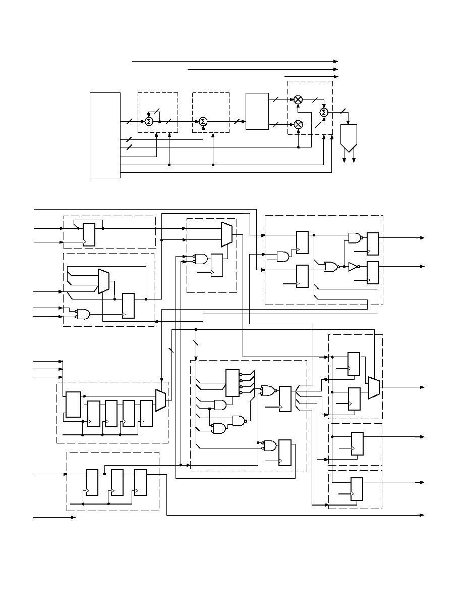
AD7008
AD7008
REGISTER
AND
CONTROL
LOGIC
32
12
20
32
12
PHASE
ACCUMULATOR
ACCUM RESET
SLEEP
AM ENABLE
PHASE
SUMMATION
12
SIN
COS
ROM
10
10
10
10
DAC
10
SIN/ COS
SUMMATION
11 PIPELINE DELAYS
13 PIPELINE DELAYS
9:0 19:10
IOUT/
IOUT
14 PIPELINE DELAYS
Figure 7. AD7008 CMOS DDS Modulator (See Table I)
CS
(27)
D0-D15
(19-26, 8-15)
TC0-TC3
ACCUMULATOR
RESET
CLK
D Q
x 6
D Q
x 6
D Q
x 6
D Q
x 6
D
Q
x 6
PASS
1
0
x 6
CLK
LOAD (36)
FSEL (31)
(32-35)
D Q
D Q
D Q
CLK
RESET (38)
RESET SYNCHRONIZATION
TRANSFER CONTROL (TC) REGISTER
CLK
D Q
x 5
TC0
TC1
LOAD
TC3
TC2
D Q
TC3
TC2
0
1
2
3
4
S
E
0
1
2
3
2
3
4
D Q
x 20
E
FREQ 0
FREQ 1
FREQUENCY
REGISTERS
PHASE REGISTER
D Q
x 12
E
CLK
D Q
x 32
E
IQ MOD REGISTER
1
0
x32
TO PHASE
SUMMATION
TO SIN/COS
SUMMATION
TO PHASE
ACCUMULATOR
CLK
CLK
CLK
32
32
12
10
TRANSFER DECODE
FSELECT
CLOCK (30)
x 5
D FLIP-FLOPS ARE MASTER SLAVE,
LATCHING DATA ON CLK RISING EDGE.
CLK
1
0
x 24
WR
(16)
SCLK (41)
SDATA (42)
SLEEP (37)
15:0 23:8
15:8 7:0
23:0
7:0
D Q
x 32
32-BIT SERIAL
ASSEMBLY REGISTER
32-BIT PARALLEL
ASSEMBLY REGISTER
D Q
x 32
REGISTER
MUX
31:0
31:0
D Q
x 4
D Q
CLK
3:0
1
0
x 32
D Q
D1
D2
BUS MODE
SYNCHRO LOGIC
D0
D3
D Q
D Q
CLK
AM ENABLE
SLEEP
COMMAND REGISTER
CLK
CLK
PASS FLIP-FLOPS ARE TRANSPARENT
WHEN THE CLOCK IS LOW.
CLK
0
1
31:8
D Q
x 32
E
5
6
Figure 8. AD7008 Register and Control Logic
AD7008
REV. B
7
Table II. Source and Destination Register
TC3
TC2
TC1
TC0
LOAD
Source Register
Destination Register
X
X
X
X
0
N/A
N/A
0
0
X
X
1
Parallel
COMMAND*
1
0
0
0
1
Parallel
FREQ0
1
0
0
1
1
Parallel
FREQ1
1
0
1
0
1
Parallel
PHASE
1
0
1
1
1
Parallel
IQMOD
1
1
0
0
1
Serial
FREQ0
1
1
0
1
1
Serial
FREQ1
1
1
1
0
1
Serial
PHASE
1
1
1
1
1
Serial
IQMOD
*The Command Register can only be loaded from the parallel assembly registers.
Table III. AD7008 Control Registers
Register
Size
Reset State
Description
COMMAND REG* 4 Bits CR3CR0
All Zeros
Command Register. This is written to using the parallel assembly register.
FREQ0 REG
32 Bits DB31DB0
All Zeros
Frequency Register 0. This defines the output frequency, when
FSELECT = 0, as a fraction of the CLOCK frequency.
FREQ1 REG
32 Bits DB31DB0
All Zeros
Frequency Register 1. This defines the output frequency, when
FSELECT = 1, as a fraction of the CLOCK frequency.
PHASE REG
12 Bits DB11DB0
All Zeros
Phase Offset Register. The contents of this register is added to the
output of the phase accumulator.
IQMOD REG
20 Bits DB19DB0
All Zeros
I and Q Amplitude Modulation Register. This defines the amplitude of
the I and Q signals as 10-bit twos complement binary fractions.
DB[19:10] is multiplied by the Quadrature (sine component and
multiplied by the In-Phase (cosine) component.
*On power up, the Command Register should be configured by the user for the desired mode before operation.
Table IV. Command Register Bits*
CR0
= 0
Eight-Bit Databus. Pins D15D8 are ignored and the parallel assembly register shifts eight places left on each write.
Hence four successive writes are required to load the 32-bit parallel assembly register, Figure 6.
= 1
Sixteen-Bit Databus. The parallel assembly register shifts 16 places left on each write. Hence two successive writes are
required to load the 32-bit parallel assembly register, Figure 5.
CR1
= 0
Normal Operation.
= 1
Low Power Sleep Mode. Internal Clocks and the DAC current sources are turned off.
CR2
= 0
Amplitude Modulation Bypass. The output of the sine LUT is directly sent to the DAC.
= 1
Amplitude Modulation Enable. IQ modulation is enabled allowing AM or QAM to be performed.
CR3
= 0
Synchronizer Logic Enabled. The FSELECT, LOAD and TC3TC0 signals are passed through a 4-stage pipeline
to synchronize them with the CLOCK, avoiding metastability problems.
= 1
Synchronizer Logic Disabled. The FSELECT, LOAD and TC3TC0 signals bypass the synchronization logic. This
allows for faster response to the control signals.
*The Command Register can only be loaded from the parallel assembly register.
Table I. Latency Table
Latency
Function
(Synchronizer Enabled CR3 = 0
1
)
FSelect
14t
1
Phase
13t
1
IQ Mod
11t
1
NOTE
1
All latencies are reduced by 4t
1
when CR3 = 1 (synchronizer disabled). 1t
1
is
equal to one pipeline delay.
REV. B
8
AD7008
CIRCUIT DESCRIPTION
The AD7008 provides an exciting new level of integration for
the RF/Communications system designer. The AD7008 com-
bines the numerically controlled oscillator (NCO), SINE/CO-
SINE look-up tables, frequency, phase and IQ modulators, and
a digital-to-analog converter on a single integrated circuit.
The internal circuitry of the AD7008 consists of four main sec-
tions. These are:
Numerically Controlled Oscillator (NCO) + Phase Modulator
SINE and COSINE Look-Up Tables
In Phase and Quadrature Modulators
Digital-to-Analog Converter
The AD7008 is a fully integrated Direct Digital Synthesis
(DDS) chip. The chip requires one reference clock, two low-
precision resistors and six decoupling capacitors to provide
digitally created sine waves up to 25 MHz. In addition to the
generation of this RF signal, the chip is fully capable of a broad
range of simple and complex modulation schemes. These
modulation schemes are fully implemented in the digital domain
allowing accurate and simple realization of complex modulation
algorithms using DSP techniques.
THEORY OF OPERATION
Sine waves are typically thought of in terms of their amplitude
form: a(t) = sin (
t) or a(t) = cos (
t). However, these are non-
linear and not easy to generate except through piece wise con-
struction. On the other hand, the angular information is linear
in nature. That is, the phase angle rotates though a fixed angle
for each unit of time. The angular rate depends on the fre-
quency of the signal by the traditional rate of:
= 2
f.
+1
0
1
2
0
MAGNITUDE
PHASE
Figure 9.
Knowing that the phase of a sine wave is linear and given a ref-
erence interval (clock period), the phase rotation for that period
can be determined.
Phase
=
dt
Solving for w:
=
Phase
dt
=
2
f
Solving for f and substituting the reference clock frequency for
the reference period:
1
f
CLOCK
=
dt
:
f
=
Phase
×
f
CLOCK
2
The AD7008 builds the output based on this simple equation.
A simple DDS chip will implement this equation with 3 major
subcircuits. The AD7008 has an extra section for I and Q
modulation.
Numerically Controlled Oscillator + Phase Modulator
This consists of two frequency select registers, a phase accumu-
lator and a phase offset register. The main component of the
NCO is a 32-bit phase accumulator which assembles the phase
component of the output signal. Continuous time signals have a
phase range 0 to 2
. Outside this range of numbers, the sinu-
soidal functions repeat themselves in a periodic manner. The
digital implementation is no different. The accumulator simply
scales the range of phase numbers into a multibit digital word.
The phase accumulator in the AD7008 is implemented with 32
bits. Therefore in the AD7008, 2
= 2
32
.
Likewise, the
Phase
term is scaled into this range of numbers 0
Phase
2
32
1.
Making these substitutions into the equation above:
f
=
Phase
×
f
CLOCK
2
32
where 0
Phase
<
2
32
With a clock signal of 50 MHz and a phase word of 051EB852
hex:
f
=
51EB852
×
50 MHz
2
32
=
1.000000000931 MHz
The input to the phase accumulator (i.e., the phase step) can be
selected either from the FREQ0 Register or FREQ1 Register,
and this is controlled by the FSELECT pin. The phase accu-
mulator in the AD7008 inherently generates a continuous 32-
bit phase signal, thus avoiding any output discontinuity when
switching between frequencies. This facilitates complex fre-
quency modulation schemes, such as GMSK.
Following the NCO, a phase offset can be added to perform
phase modulation using the 12-bit PHASE Register. The con-
tents of this register are added to the most significant bits of the
NCO.
Sine and Cosine Look-Up Tables
To make the output useful, the signal must be converted from
phase information into a sinusoidal value. Since phase informa-
tion maps directly into amplitude, a ROM look up table con-
verts the phase information into amplitude. To do this the
digital phase information is used to address a Sine/Cosine ROM
LUT. Only the most significant 12 bits are used for this pur-
pose. The remaining 20 bits provide frequency resolution and
minimize the effects of quantization of the phase to amplitude
conversion.
In Phase and Quadrature Modulators
Two 10-bit amplitude multipliers are provided allowing the easy
implementation of either Quadrature Amplitude Modulation
(QAM) or Amplitude Modulation (AM). The 20-bit IQMOD
Register is used to control the amplitude of the I (cos) and Q
(sin) signals. IQMOD [9:0] controls the I amplitude and
IQMOD [19:10] controls the Q amplitude.
The user should ensure that when summing the I and Q signals
the sum should not exceed the value that a 10-bit accumulator
can hold. The AD7008 does not clip the digital output; the
output will roll over instead of clip.
AD7008
REV. B
9
When amplitude modulation is not required, the IQ multipliers
can be bypassed (CR = 2). The sine output is directly sent to
the 10-bit DAC.
Digital-to-Analog Converter
The AD7008 includes a high impedance current source 10-bit
DAC, capable of driving a wide range of loads at different
speeds. Full-scale output current can be adjusted, for optimum
power and external load requirements, through the use of a
single external resistor (R
SET
).
The DAC can be configured for single or differential-ended
operation. IOUT can be tied directly to AGND for single-ended
operation or through a load resistor to develop an output volt-
age. The load resistor can be any value required as long as the
full-scale voltage developed across it does not exceed 1 volt.
Since full-scale current is controlled by R
SET
, adjustments to
R
SET
can balance changes made to the load resistor.
DSP and MPU Interfacing
The AD7008 contains a 32-bit parallel assembly register and a
32-bit serial assembly register. Each of the modulation registers
can be loaded from either assembly register under control of the
LOAD pin and the Transfer-Control (TC) pins (See Table II).
The Command register can be loaded only from the parallel as-
sembly register. In practical use, both serial and parallel inter-
faces can be used simultaneously if the application requires.
TC3TC0 should be stable before the LOAD signal rises and
should not change until after LOAD falls (Figure 2).
The DSP/MPU asserts both WR and CS to load the parallel as-
sembly register (Figure 3). At the end of each write, the parallel
assembly register is shifted left by 8 or 16 bits (Depending on
CR0), and the new data is loaded into the low bits. Hence, two
16-bit writes or four 8-bit writes are used to load the parallel as-
sembly register. When loading parallel data, it is only necessary
to write as much data as will be used by that register. For in-
stance, the Command Register requires only one write to the
parallel assembly register.
Serial data is input to the chip on the rising edge of SCLK, most
significant bit first (Figure 4). The data in the assembly regis-
ters can be transferred to the modulation registers by means of
the transfer control pins.
Maximum Updating of the AD7008
Updating the AD7008 need not take place in a synchronous
fashion. However, in asynchronous systems, most of the exter-
nal clock pulses (LOAD and SCLK) must be high for greater
than one system clock period. This insures that at least one
CLOCK rising edge will occur successfully completing the latch
function (Figure 1).
However, if the AD7008 is run in a synchronous mode with the
controlling DSP or microcontroller, the AD7008 may be loaded
very rapidly. Optimal speed is attained when operated in the
16-bit load mode; the following discussion will assume that
mode is used. Each of the modulation registers require two 16
bit loads. This data is latched into the parallel assembly register
on the falling edge of the WR command. This strobe is not
qualified by the CLOCK pulse but must be held low for a mini-
mum of 20 ns and only need be high for 10 ns. The two 16-bit
words may be loaded in succession. While the second 16-bit
word is being latched into the parallel assembly register, the
Transfer and Control word may be presented to the TC3TC0
pins. If the designation register is always the same, an external
register can be used to store the information on the inputs of
TC3TC0. At some time after the second falling edge of WR,
the LOAD signal may go high. As long as the load signal is high
5 ns (see setup time) before the rising edge of the CLOCK sig-
nal, data will be transferred to the destination register.
The limiting factor of this technique is the WR period which is
30 ns. Thus the CLOCK may run up to 33 MSPS using this
technique and the effective update rate would be one half or
16.5 MHz. See timing Figure 10 for timing details.
DATA
HI WORD
WR
LOW WORD
CLOCK
TC
LOAD
Figure 10. Accelerated Data Load Sequence
APPLICATIONS
Serial Configuration
Data is written to the AD7008 in serial mode using the two sig-
nal lines SDATA and SCLK. Data is accumulated in the serial
assembly register with the most significant bit loaded first. The
data bits are loaded on the rising edge of the serial clock. Once
data is loaded in the serial assembly register, it must be trans-
ferred to the appropriate register on chip. This is accomplished
by setting the TC bits according to Tables II and III. If you
want to load the serial assembly register into FREQ1 register,
the TC bits should be 1101. When the LOAD pin is raised,
data is transferred directly to the FREQ1 register. When oper-
ating in serial mode, some functions must still operate in parallel
mode such as loading the TC bits and updating the Command
register which is accessed only through the parallel assembly
register. See Figure 11 for a typical serial mode configuration.
R5
390
C2
0.1µF
CMD0
CMD1
CMD2
CMD3
19
20
21
22
23
24
25
26
8
9
10
11
12
13
14
15
16
D0
D1
D2
D3
D4
D5
D6
D7
D8
D9
D10
D11
D12
D13
D14
D15
WR
TC0
TC1
TC2
TC3
WR
LOAD
SCLK
SDATA
RESET
V
CC
V
EE
50MHz
U2
+5V
K1115
7
14
OUT
V
REF
COMP
IOUT
IOUT
FSADJUST
V
AA
V
DD
V
DD
V
DD
AGND
DGND
DGND
DGND
DGND
TEST
44
7
18
29
43
40
3
17
28
39
+5V
+5V
+5V
+5V
4
5
6
C1
0.1µF
+5V
+5V
R4
49.9
2
1
R3
49.9
U3
AD7008
8
TC0
TC1
TC2
TC3
LOAD
SCLK
SDATA
FSELECT
CLK
RESET
SLEEP
CS
27
32
33
34
35
36
41
42
31
30
38
37
Figure 11. General Purpose Serial Interface
REV. B
10
AD7008
Parallel Configuration
The AD7008 functions fully in the parallel mode. There are
two parallel modes of operation. Both are similar but are tai-
lored for different bus widths, 8 and 16 bits. All modes of op-
eration can be controlled by the parallel interface.
On power up and reset, the chip must be configured by instruc-
ting the command register how to operate. The command reg-
ister may be used to set the device up for 8- or 16-bit mode,
RF
INPUT
(ANTENNA)
330
330
4.7
µF
100
nF
100
nF
MIDPOINT
BIAS
GENERATOR
OPTIONAL
BPF
OR LPF
VMID
10
10
BANDPASS
FILTER
AGC
DETECTOR
PLL
90
°
0
°
FM OUTPUT
AM OUTPUT
BIAS
CIRCUIT
PTAT
VOLTAGE
AGC VOLTAGE
PLL INPUT
RECEIVED
SIGNAL
STRENGTH
INDICATOR
R
SET
390
5
5
AD7008
FILTER
0.1µF
16dBm
10 BITS
AD607
Figure 13. AD7008 and AD607 Receiver Circuit
sleep mode, amplitude control and synchronization logic. At
reset, the chip defaults to 8-bit bus, no amplitude control and
logic synchronized. The code fragment below indicates how
the initialization code for the AD7008 might look using the
ADSP-21020.
{dds_para is a port define to decode for
the parallel assembly register write pulse.
dds_cont is a port defined to decode for
the TC control Load pin. The Command reg-
ister must first be loaded with configura-
tion information. In this example, the chip
is set up for 16 bits data. See Table III
for details.}
r4 = 0x00010000;
{16 bits, Normal Op., AM
disabled, Synchronizer
enabled}
dm(dds_para) = r4; {write data to parallel
assembly register}
r4 = 0x00000000;
dm(dds_cont) = r5; {No data written, data is
just transferred from
parallel assembly
register to the command
register}
r4 = 0x051E0000;
{1 MHz=051EB852, load high
word first}
dm(dds_para) = r4;
r4 = 0xB8520000;
{Now load low word}
dm(dds_para)=r4;
r4 = 0x80000000; {Transfer data from the
parallel assembly
register to Freq0}
dm(dds_cont)=r4;
Local Oscillator
The AD7008 is well suited for applications such as local oscilla-
tors used in super-heterodyne receivers. Although the AD7008
can be used in a variety of receiver designs, one simple local os-
C1
0.1µF
6
4
5
Y7
Y6
Y5
Y4
Y3
Y2
Y1
Y0
7
9
10
11
12
13
14
15
G1
G
2A
G
2B
+5V
DMS1
DMWR
R5
390
C2
0.1µF
DMD24
DMD25
DMD26
DMD27
DMD28
DMD29
DMD30
DMD31
DMD32
DMD33
DMD34
DMD35
DMD36
DMD37
DMD38
DMD39
19
20
21
22
23
24
25
26
8
9
10
11
12
13
14
15
16
TC0
TC1
TC2
TC3
LOAD
SCLK
SDATA
FSELECT
CLK
RESET
SLEEP
CS
GND
DMD36
DMD37
DMD38
DMD39
RESET
V
CC
V
EE
50MHz
U2
+5V
K1115
7
14
OUT
V
REF
COMP
IOUT
IOUT
FSADJUST
V
AA
V
DD
V
DD
V
DD
AGND
DGND
DGND
DGND
DGND
TEST
44
7
18
29
43
40
3
17
28
39
+5V
+5V
+5V
+5V
4
5
6
+5V
+5V
R4
49.9
2
1
R3
49.9
C
B
A
DMA02
DMA01
DMA00
3
2
1
U1
74HC138
U3
AD7008
8
DMDXXDATA BITS
DMAXXADDRESS BITS
D0
D1
D2
D3
D4
D5
D6
D7
D8
D9
D10
D11
D12
D13
D14
D15
WR
27
32
33
34
35
36
41
42
31
30
38
37
Figure 12. Parallel Interface to a 16- or 32-Bit DSP or
Microprocessor
AD7008
REV. B
11
{This section converts the twos complement au-
dio into offset binary scaled for modulating
the AD7008. If twos complement is used, the
modulation scheme will instead be double side-
band, suppressed carrier.}
r5 = 0x80000000;
r6 = r6 xor r5;
r6 = lshift r6 by -1;
r6 = r6 xor r5;
r4 = lshift r6 by -6;
{Load parallel assembly register with modula-
tion data. Q portion set to midscale, I
portion with scaled data}
r5 = 0x00000004;
dm(dds_para) = r5;
dm(dds_para) = r4;
{Transfer parallel assembly register to IQMOD
register}
r4 = 0xb0000000;
dm(dds_cont) = r4;
rti;
Many applications require precise control of the output ampli-
tude, such as in local oscillators, signal generators and modula-
tors. There are several methods to control signal amplitude.
The most direct is to program the amplitude using the IQMOD
register on the AD7008. Other methods include selecting the
load resistor value or changing the value of R
SET
. Another op-
tion is to place a voltage out DAC on the ground side of R
SET
as
in Figure 16. This allows easy control of the output amplitude
without affecting other functions of the AD7008. Any combina-
tion of these techniques may be used as long as the full-scale
voltage developed across the load does not exceed 1 volt.
cillator application is with the AD607 Monoceiver(tm). This
unique two chip combination provides a complete receiver sub-
system with digital frequency control, RSSI and demodulated
outputs for AM, FM and complex I/Q (SSB or QAM). (See
Figure 13.)
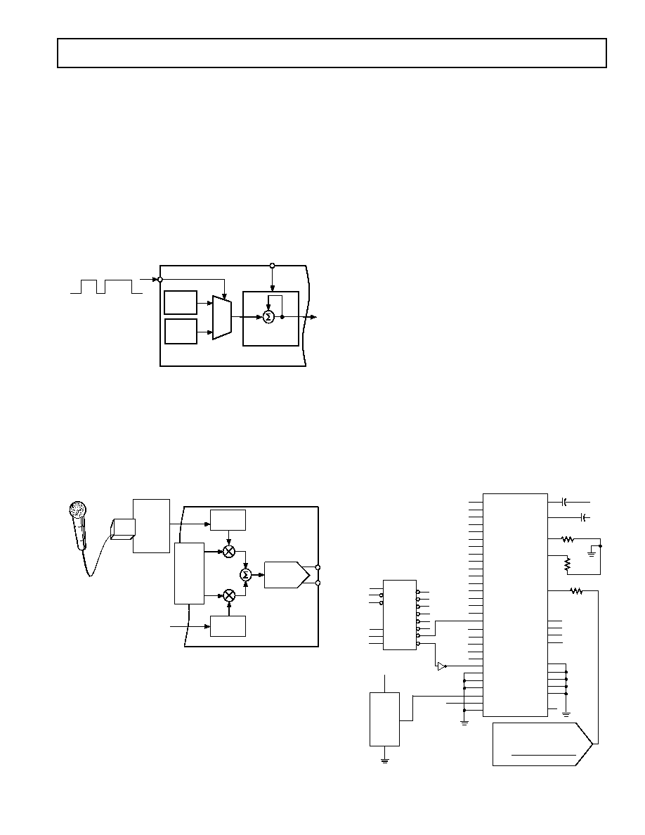
Direct Digital Modulator
In addition to the basic DDS function provided by the AD7008,
the device also offers several modulation capabilities useful in a
wide variety of application. The simplest modulation scheme is
frequency shift keying or FSK. In this application, each of the
two frequency registers is loaded with a different value, one rep-
resenting the space frequency and the other the mark frequency.
The digital data stream is fed to the FSELECT pin causing
the AD7008 to modulate the carrier frequency between the two
values.
FREQ 0
REG
FREQ 1
REG
32
32
32
MUX
32
0
1
1
0
0
F SELECT
CLOCK
PHASE
ACCUMULATOR
AD7008
Figure 14. FSK Modulator
The AD7008 has three registers that can be used for modula-
tion. Besides the example of frequency modulation shown
above, the frequency registers can be updated dynamically as
can the phase register and the IQMOD register. These can be
modulated at rates up to 16.5 MHz. The example shown below
along with code fragment shows how to implement the AD7008
in an amplitude modulation scheme. Other modulation
schemes can be implemented in a similar fashion.
SIN/COS
ROM
SIN
COS
DSP:
SCALE
ANALOG
INPUT TO
FULL
SCALE
I MOD
ADC
Q MOD
10
10
10
10
10
10
10-BIT DAC
IOUT
IOUT
10
10
0
AD7008
Figure 15. Amplitude Modulation
{__________IRQ3 Interrupt Vector__________}
{in_audio is a port used to sample the audio
signal. This signal is assumed to be twos
complement. This interrupt should be serviced
at an audio sample rate. This routine assumes
that the AD7008 has been set up with the Ampli-
tude Modulation Enabled.}
irq3_asserted:
{Get audio sample}
r6=dm(in_audio);
C1
0.1µF
6
4
5
Y7
Y6
Y5
Y4
Y3
Y2
Y1
Y0
7
9
10
11
12
13
14
15
G1
G
2A
G
2B
+5V
DMS1
DMWR
R5
390
C2
0.1µF
DMD24
DMD25
DMD26
DMD27
DMD28
DMD29
DMD30
DMD31
DMD32
DMD33
DMD34
DMD35
DMD36
DMD37
DMD38
DMD39
19
20
21
22
23
24
25
26
8
9
10
11
12
13
14
15
16
DMS3
DMD36
DMD37
DMD38
DMD39
RESET
V
CC
V
EE
50MHz
U2
+5V
K1115
7
14
OUT
V
REF
COMP
IOUT
IOUT
FSADJUST
V
AA
V
DD
V
DD
V
DD
AGND
DGND
DGND
DGND
DGND
TEST
44
7
18
29
43
40
3
17
28
39
+5V
+5V
+5V
+5V
4
5
6
+5V
+5V
R4
49.9
2
1
R3
49.9
C
B
A
DMA02
DMA01
DMA00
3
2
1
U1
74HC138
U3
AD7008
8
VOLTAGE OUT DAC,
i.e., AD7245A
0 TO +1 VOLTS
Ifs = 6233 x (V
REF
V
DAC
)
R
SET
DMDXXDATA BITS
DMAXXADDRESS BITS
CS
TC0
TC1
TC2
TC3
LOAD
SCLK
SDATA
FSELECT
CLK
RESET
SLEEP
D0
D1
D2
D3
D4
D5
D6
D7
D8
D9
D10
D11
D12
D13
D14
D15
WR
27
32
33
34
35
36
41
42
31
30
38
37
Figure 16. External Gain Adjustment
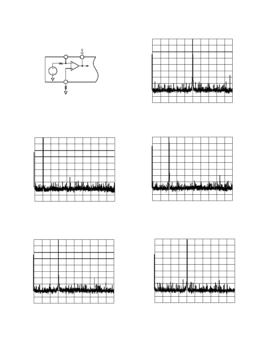
AD7008Typical Performance Characteristics
START 0 Hz
RBW 3 kHz
VBW 10 kHz
STOP 10 000 000.0 Hz
ST 2.4 SEC
REF 5.0 dBm
10 dB/DIV
RANGE 5.0 dBm
OFFSET 4 640 000.0 Hz
54.8 dB
Figure 20. f
CLK
= 20 MHz, f
OUT
= 5.1 MHz
START 0 Hz
RBW 3 kHz
VBW 10 kHz
STOP 10 000 000.0 Hz
ST 2.4 SEC
REF 4.3 dBm
10 dB/DIV
RANGE 5.0 dBm
OFFSET 6 320 000.0 Hz
61.3 dB
Figure 21. f
CLK
= 20 MHz, f
OUT
= 2.1 MHz
START 0 Hz
RBW 3 kHz
VBW 10 kHz
STOP 10 000 000.0 Hz
ST 2.4 SEC
REF 5.0 dBm
10 dB/DIV
RANGE 5.0 dBm
OFFSET 490 000.0 Hz
63.4 dB
Figure 22. f
CLK
= 20 MHz, f
OUT
= 4.1 MHz
REV. B
12
V
REF
6
4
5
V
REF
+5V
TO DAC
COMP
R
SET
AD7008
115
TYP
Figure 17. Equivalent Reference Circuit
START 0 Hz
RBW 3 kHz
VBW 10 kHz
STOP 10 000 000.0 Hz
ST 2.4 SEC
REF 4.3 dBm
10 dB/DIV
RANGE 5.0 dBm
OFFSET 3 330 000.0 Hz
63.6 dB
Figure 18. f
CLK
= 20 MHz, f
OUT
= 1.1 MHz
START 0 Hz
RBW 3 kHz
VBW 10 kHz
STOP 10 000 000.0 Hz
ST 2.4 SEC
REF 4.3 dBm
10 dB/DIV
RANGE 5.0 dBm
OFFSET 4 500 000.0 Hz
61.1 dB
Figure 19. f
CLK
= 20 MHz, f
OUT
= 3.1 MHz
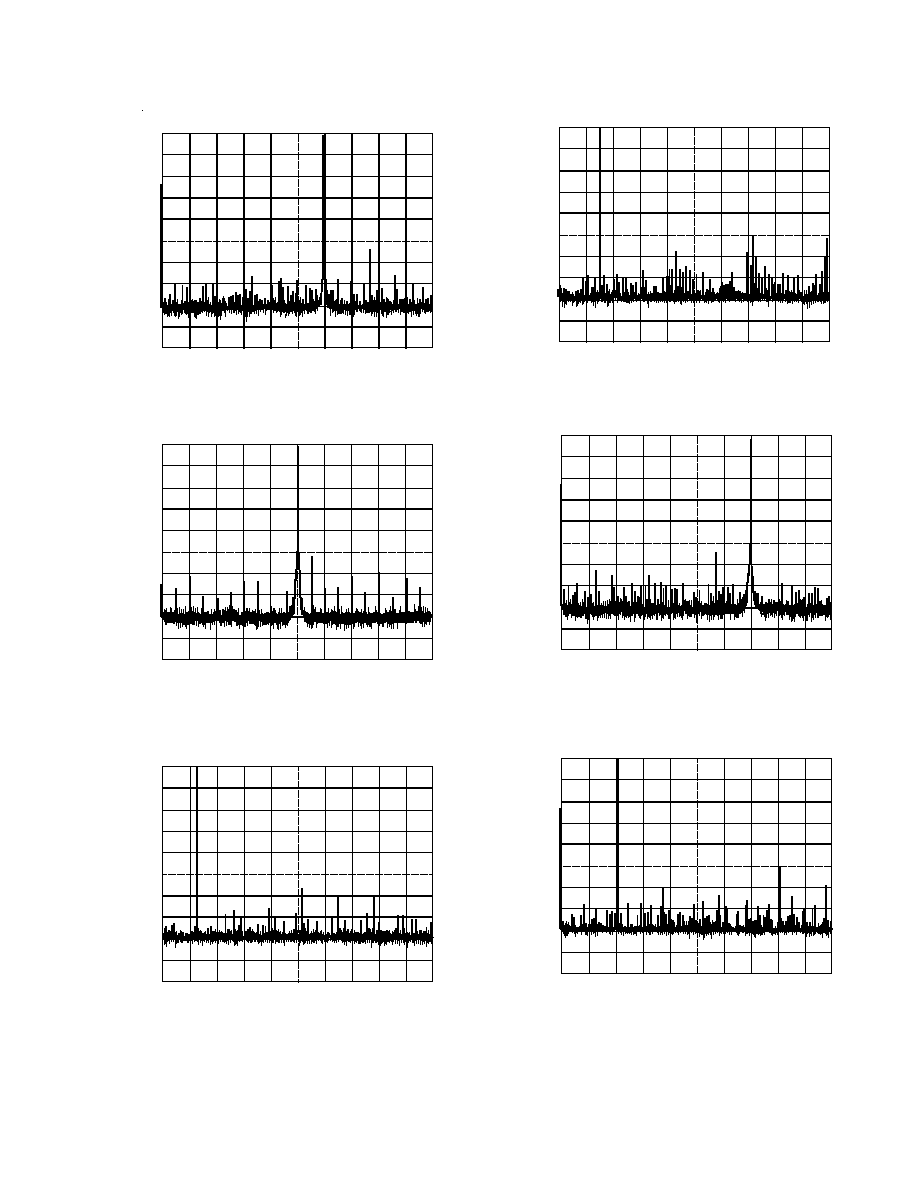
START 0 Hz
RBW 3 kHz
VBW 10 kHz
STOP 10 000 000.0 Hz
ST 2.4 SEC
REF 5.0 dBm
10 dB/DIV
RANGE 5.0 dBm
OFFSET 1 680 000.0 Hz
52.8 dB
Figure 23. f
CLK
= 20 MHz, f
OUT
= 6.1 MHz
CENTER 6 500 000.0 Hz
RBW 3 kHz
VBW 10 kHz
SPAN 10 000 000.0 Hz
ST 2.4 SEC
REF 4.3 dBm
10 dB/DIV
RANGE 5.0 dBm
OFFSET 500 000.0 Hz
51.7 dB
Figure 24. f
CLK
= 20 MHz, f
OUT
= 6.5 MHz
VBW 10 kHz
STOP 16 000 000.0 Hz
ST 3.6 SEC
REF 4.3 dBm
10 dB/DIV
RANGE 5.0 dBm
OFFSET 6 304 000.0
Hz56.3 dB
START 0 Hz
RBW 3 kHz
Figure 25. f
CLK
= 50 MHz, f
OUT
= 2.1 MHz
CENTER 16 000 000.0 Hz
RBW 3 kHz
REF 4.3 dBm
10 dB/DIV
RANGE 5.0 dBm
OFFSET 14 500 000.0 Hz
52.4 dB
VBW 10 kHz
SPAN 25 000 000.0 Hz
ST 5.6 SEC
Figure 26. f
CLK
= 50 MHz, f
OUT
= 7.1 MHz
VBW 10 kHz
STOP 10 000 000.0 Hz
ST 2.4 SEC
REF 5.0 dBm
10 dB/DIV
RANGE 5.0 dBm
OFFSET 1 280 000.0 Hz
51.8 dB
START 0 Hz
RBW 3 kHz
Figure 27. f
CLK
= 20 MHz, f
OUT
= 7.1 MHz
VBW 10 kHz
STOP 25 000 000.0 Hz
ST 5.6 SEC
REF 4.3 dBm
10 dB/DIV
RANGE 5.0 dBm
START 0 Hz
RBW 3 kHz
OFFSET 15 300 000.0 Hz
51.8 dB
Figure 28. f
CLK
= 50 MHz, f
OUT
= 5.1 MHz
Typical Performance CharacteristicsAD7008
REV. B
13
START 0 Hz
RBW 3 kHz
VBW 10 kHz
STOP 25 000 000.0 Hz
ST 5.6 SEC
REF 5.0 dBm
10 dB/DIV
RANGE 5.0 dBm
OFFSET 4 500 000.0 Hz
54.7 dB
Figure 29. f
CLK
= 50 MHz, f
OUT
= 9.1 MHz
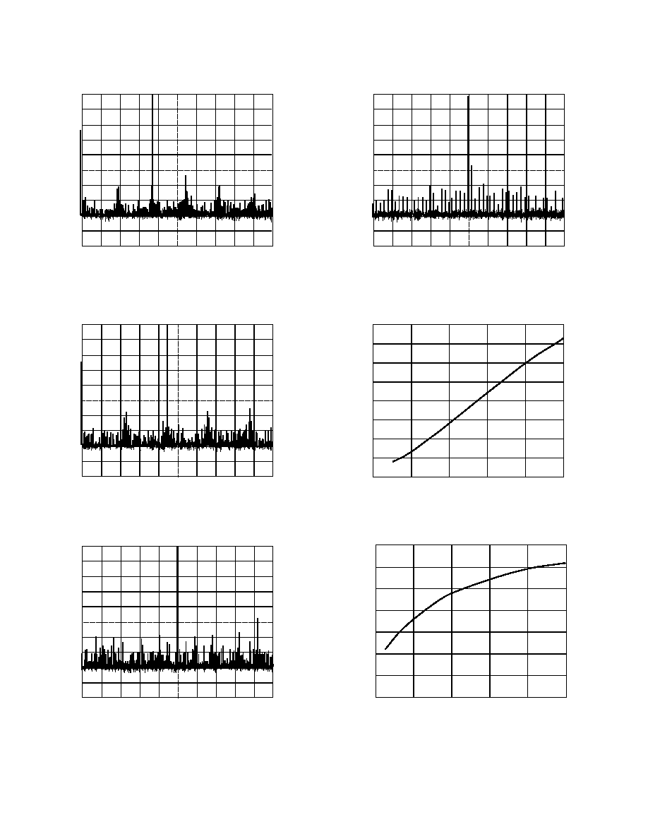
START 0 Hz
RBW 3 kHz
VBW 10 kHz
STOP 25 000 000.0 Hz
ST 5.6 SEC
REF 5.0 dBm
10 dB/DIV
RANGE 5.0 dBm
OFFSET 11 100 000.0 Hz
54.1 dB
CENTER 13 100 000.0 Hz
RBW 3 kHz
VBW 10 kHz
SPAN 25 000 000.0 Hz
ST 5.6 SEC
REF 5.0 dBm
10 dB/DIV
RANGE 5.0 dBm
OFFSET 10 675 000.0 Hz
47.0 dB
Figure 31. f
CLK
= 50 MHz, f
OUT
= 13.1 MHz
Figure 30. f
CLK
= 50 MHz, f
OUT
= 11.1 MHz
CENTER 16 500 000.0 Hz
RBW 3 kHz
VBW 10 kHz
SPAN 25 000 000.0 Hz
ST 5.6 SEC
REF 5.0 dBm
10 dB/DIV
RANGE 5.0 dBm
OFFSET 500 000.0 Hz
44.8 dB
130
50
50
70
60
10
0
90
80
100
110
120
40
30
20
MASTER CLOCK MHz
TOTAL CURRENT I
AA
+ I
DD
mA
Figure 32. f
CLK
= 50 MHz, f
OUT
= 16.5 MHz
Figure 33. Typical Current Consumption vs. Frequency
Figure 34. Typical Plot of SFDR vs. Master Clock Frequency
When f
OUT
= 1/3f
CLK
, Frequency Word = 5671C71C Hex
40
75
50
60
70
10
65
0
45
55
50
40
30
20
MASTER CLOCK MHz
WIDEBAND SFDR dB
REV. B
14
AD7008Typical Performance Characteristics
AD7008
REV. B
15
AD7008/PCB DDS EVALUATION BOARD
The AD7008/PCB DDS Evaluation Board allows designers to
evaluate the high performance AD7008 DDS Modulator with a
minimum amount of effort.
To prove this DDS will meet the user's waveform synthesis re-
quirements, the only things needed are the AD7008/PCB DDS
Evaluation Board, +5 V power supply, an IBM-compatible PC,
and a spectrum analyzer. The evaluation setup is shown below.
The DDS evaluation kit includes a populated, tested AD7008/
PCB board; software which controls the AD7008 through the
parallel printer port in a DOS or Windows environment and an
AD7008P.
The AD7008 direct digital synthesis chip is a numerically
controlled oscillator employing a 32-bit phase accumulator, sine
and cosine look-up tables, and a l0-bit D/A converter integrated
on a single CMOS chip. Modulation capabilities are provided
for phase modulation, frequency modulation, and both in-phase
and quadrature amplitude modulation suitable for SSB
generation.
Clock rates up to 20 MHz and 50 MHz are supported. Fre-
quency accuracy can be controlled to one part in four billion.
+5V
SOFTWARE
PROVIDED
POWER
SUPPLY
INTERFACE
EXTERNAL
POWER
SUPPLY
STANDARD
PRINTER
CABLE
IBM-COMPATIBLE PC
AD7008
50MHz
CMOS DDS
INTERFACE
LOGIC
50
CABLE
SPECTRUM ANALYZER
AD7008 DDS EVALUATION BOARD
OPTIONAL
TTL CLOCK
REFERENCE
GENERATOR
CLOCK
OSCILLATOR
Figure 35. AD7008 DDS Evaluation Board Setup
Table IV. AD7008/PCB Typical Electrical Characteristics
(Nominal power supplies, CLK = 50 MHz)
Typical
Characteristics
Value
Units
+5.0 V Supply Current
125
mA
AD7008 Output Voltage
0 to +1.0
V
(Terminated into 50
Externally)
CMOS clock input HIGH
4.1 to 5
V
CMOS clock input LOW
0.0 to 0.5
V
USING THE AD7008/PCB DDS EVALUATION BOARD
The AD7008/PCB evaluation kit is a test system designed to
simplify the evaluation of the AD7008 50 MHz Direct Digital
Synthesizer. Provisions to control the AD7008 from the printer
port of an IBM-compatible PC are included, along with the
necessary software. This data sheet provides information on
operating the evaluation board; additional details are available
from the ADI technical assistance line 1-800-ANALOGD.
Prototyping Area
An area near one edge of the board is intentionally left void of
components to allow the user to add additional circuits to the
evaluation test set. Users may want to build custom analog fil-
ters for the outputs, or add buffers and operational amplifiers
used in the final applications.
XO vs. External Clock
The reference clock of the AD7008/PCB is normally provided
by a 50 MHz CMOS oscillator. This oscillator can be removed
and an external CMOS clock connected to CLOCK. If an ex-
ternal clock is used, a 50
resistor R6 should be installed.
Power Supply
Power for the AD7008/PCB must be provided externally
through the pin connections, as described in the Inputs/Outputs.
The power leads should be twisted to reduce ground loops.
AD7008/PCB BILL OF MATERIAL
Quantity
Reference
Description
1
C1
Tag Tant Cap, 10
µ
F, 35 V, 20%
8
C2C9
Cer Chip Cap, 0.1
µ
F, Murata
Grm42
6
CLOCK, FSEL SMB Submin Snap-on (Male)
I
OUT
, I
OUTN
PCB MT Plug
SCLK, SDATA
1
FSADJ
RN55 Res Met Film, 392
1
LK1
HDR SIP 3-Pin Male
1
Shunt 530153-2
1
P1
36-Pin D Conn Rt Ang Pcmt
Fem AMP
1
P2
PC Voltage Ter Blk w/Screws
Augat RDI
3
R1R3
RN55 Res Met Film, 10k
2
R4, R5
RN55 Res Met Film, 49.9
1
RZ1
10P Bussed Res Ntwk, 10k
CSC10A01103G
1
RZ2
6P Bussed Res Ntwk, 4.7k
CSC06A01472G
1
U1
AD7008 JP50 CMOS DDS
Modulator
1
U2
74HC74 Dual D-type Pos-Ed-
Trigd Flip-Flop
1
V
REF
Pin Terminal, Testpoint
1
XTAL
OSC XTAL, Fox F1100H
50 MHz
1
Socket, Methode 213-044-501
4
Support, Nylon
1
PCB, 48295(-)
26
Pin Sockets, Closed End
REV. B
16
AD7008
A 3.5" floppy disk containing software to control the AD7008 is
provided with the AD7008/PCB. This software was developed
using C. The C source code is provided in a file named
A:\AD7008.C, which the user may view, run, or modify.
An executable version of this software is also provided, and can
be executed from DOS by typing "A:\AD7008." The software
prompts the user to provide the necessary information needed
by the program. Additional information is included in a test file
named A:\readme.txt.
A windows 3.1 executable called WIN7008 is also included.
OUTLINE DIMENSIONS
Dimensions shown in inches and (mm).
44-Pin PLCC (P-44A)
6
PIN 1
IDENTIFIER
7
40
39
17
18
29
28
TOP VIEW
(PINS DOWN)
0.695 (17.65)
0.685 (17.40)
SQ
0.656 (16.66)
0.650 (16.51)
SQ
0.048 (1.21)
0.042 (1.07)
0.048 (1.21)
0.042 (1.07)
0.020
(0.50)
R
0.021 (0.53)
0.013 (0.33)
0.050
(1.27)
BSC
0.63 (16.00)
0.59 (14.99)
0.032 (0.81)
0.026 (0.66)
0.180 (4.57)
0.165 (4.19)
0.040 (1.01)
0.025 (0.64)
0.056 (1.42)
0.042 (1.07)
0.025 (0.63)
0.015 (0.38)
0.110 (2.79)
0.085 (2.16)
INPUTS/OUTPUTS
Name
Description
P1
36-pin edge connector to connect to parallel
port of PC.
CLOCK
CMOS input for clock R6 provides termination.
FSEL
CMOS input to select between Freq 0 and Freq 1.
Low selects Freq 0.
SDATA
CMOS input for serial input pin.
SCLK
CMOS input for clocking in SDATA.
I
OUT
Analog output.
I
OUT
N
Complementary analog output.
V
REF
Test point for V
REF
pin.
P2
+5 V and ground power connection.
LK1
External sleep command input.
Figure 36.
Controlling the AD7008/PCB
The AD7008/PCB is designed to allow control (frequency
specification, reset, etc.) through the parallel printer port of a
standard IBM-compatible PC. The user simply disconnects the
printer cable from the printer and inserts it into edge connector
P1 of the evaluation board.
The printer port provides information to the AD7008/PCB
through eight data lines and four control lines. Control signals
are latched on the AD7008/PCB to prevent problems with long
printer cables.
PRINTED IN U.S.A.
C1791a102/95
V
CC
OUT
+5V
14
7
XTAL1
8
C9
0.1µF
V
EE
PR
Q
Q
CL
C
D
>
PR
Q
Q
CL
C
D
>
LATCH
LOAD
2
3
4
5
6
8
9
10
11
12
13
1
LLOAD
WR
+5V
+5V
+5V
+5V
U2
74HC74
U2
74HC74
L
WR
C36DRPF
P1
1
2
3
4
5
6
7
8
9
10
11
12
13
14
15
16
17
18
19
20
21
22
23
24
25
26
27
28
29
30
31
32
33
34
35
36
LATCH
D0
D1
D2
D3
D4
D5
D7
D6
RESET
LOAD
WR
2
3
4
5
6
7
8
9
10
D0
D1
D2
D3
D4
D5
D7
D6
10k
10PB+5
RZ1
2
3
4
5
6
LATCH
RESET
LOAD
WR
4.7k
6PB+5
RZ2
U1
DUT7008P
6
5
2
1
4
3
17
28
39
44
7
18
29
43
40
V
REF
COMP
FSADJUST
19
20
21
22
23
24
25
26
8
9
10
11
12
13
14
15
16
27
32
33
34
35
36
41
42
31
30
38
37
D0
D1
D2
D3
D4
D5
D7
D6
RESET
1
2
3
H3M
LK1
+5V
GND
+5V
+5VD
1
2
P2
PCTB2
D8
D9
D10
D11
D12
D13
D15
D14
R1
10k
SMB
SCLK
R2
10k
R3
10k
SMB
FSELECT
R6
50
OPTIONAL
WR
CS
TC0
TC2
TC1
TC3
LOAD
SCLK
SDATA
FSELECT
CLK
SLEEP
D0
D1
D2
D3
LLOAD
RESET
DGND
DGND
DGND
DGND
AGND
TEST
+5V
+5V
+5V
+5V
C7
0.1µF
+5V
R4
50
SMB
I
OUT
FSADJ
390
L
WR
SMB
SDATA
SMB
CLK
I
OUT
I
OUT
V
REF
SMB
I
OUT
R5
50
C6
0.1µF
C2
0.1µF
C3
0.1µF
C4
0.1µF
C5
0.1µF
C1
10µF
C8
0.1µF
D0
D1
D2
D3
D4
D5
D7
D6
V
AA
V
DD
V
DD
V
DD