 | ÐлекÑÑоннÑй компоненÑ: AD7011ARS | СкаÑаÑÑ:  PDF PDF  ZIP ZIP |
Äîêóìåíòàöèÿ è îïèñàíèÿ www.docs.chipfind.ru
REV. B
Information furnished by Analog Devices is believed to be accurate and
reliable. However, no responsibility is assumed by Analog Devices for its
use, nor for any infringements of patents or other rights of third parties
which may result from its use. No license is granted by implication or
otherwise under any patent or patent rights of Analog Devices.
a
CMOS, ADC /4 DQPSK
Baseband Transmit Port
AD7011
One Technology Way, P.O. Box 9106, Norwood, MA 02062-9106, U.S.A.
Tel: 617/329-4700
Fax: 617/326-8703
FEATURES
Single +5 V Supply
On-Chip /4 DQPSK Modulator
Modulator Bypass Analog Mode
Root-Raised Cosine Tx Filters, = 0.35
Two 10-Bit D/A Converters
4th Order Reconstruction Filters
Differential Analog Outputs
On-Chip Ramp Up/Down Power Control
On-Chip Tx Offset Calibration
Dual Mode Operation, Analog and Digital
Very Low Power Dissipation, 30 mW typical
Power Down Mode < 10
A
On-Chip Voltage Reference
24-Pin SSOP
APPLICATIONS
American Digital Cellular Telephony
American Analog Cellular Telephony
GENERAL DESCRIPTION
The AD7011 is a complete low power, CMOS,
/4 DQPSK
modulator with single +5 V power supply. The part is designed
to perform the baseband conversion of I and Q transmit wave-
forms in accordance with the American Digital Cellular Tele-
phone system (TIA IS-54).
The on-chip
/4 Differential Quadrature Phase Shift Keying
(DQPSK) digital modulator, which includes the root raised
cosine filters, generates I and Q data in response to the transmit
data stream. The AD7011 also contains ramp control envelope
logic to shape the I and Q output waveforms when ramping up
or down at the beginning or end of a transmit burst.
Besides providing all the necessary logic to perform
/4 DQPSK
modulation, the part also provides reconstruction filters to
smooth the DAC outputs, providing continuous time analog
outputs. The AD7011 generates differential analog outputs for
both the I and Q signals.
As it is a necessity for all digital mobile systems to use the lowest
possible power, the device has transmit and receive power-down
options. The AD7011 is housed in a space efficient 24-pin
SSOP (Shrink Small Outline Package).
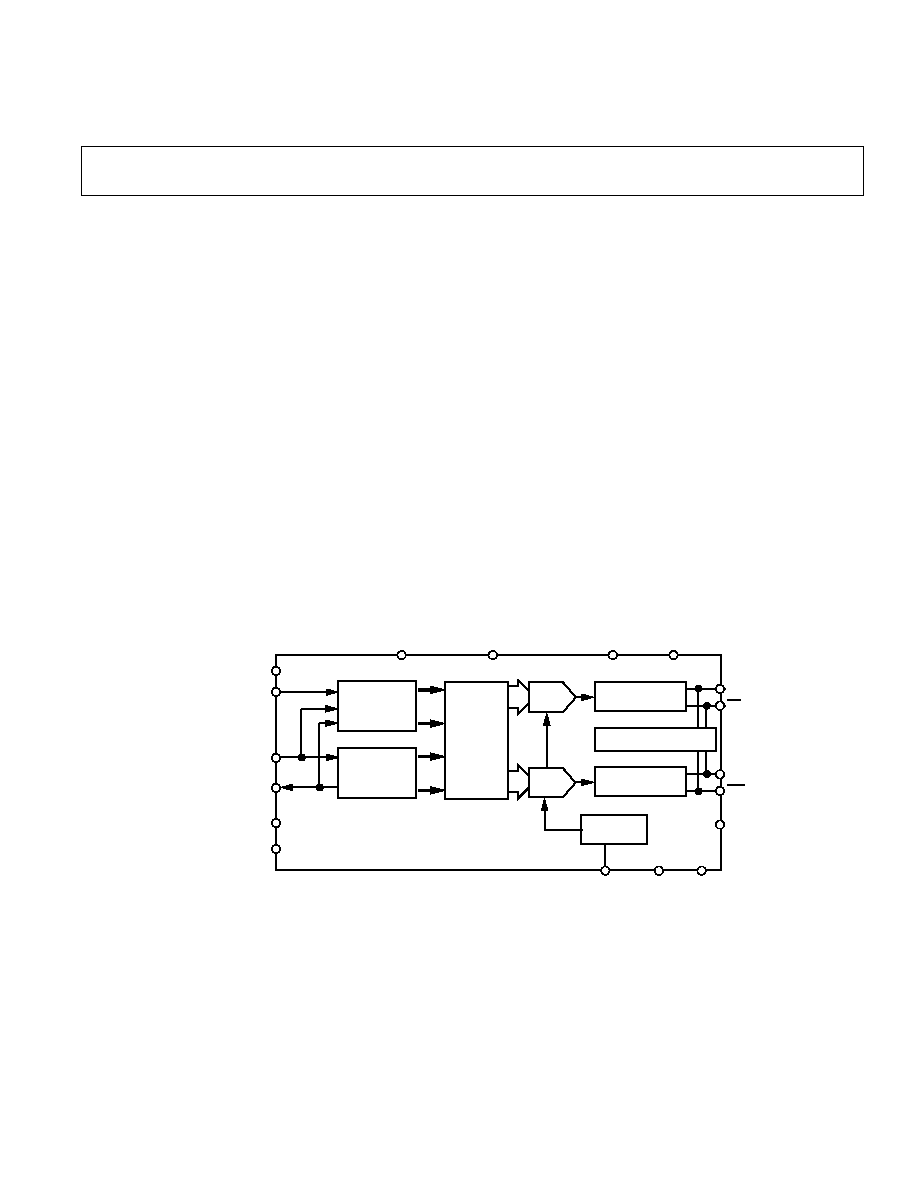
FUNCTIONAL BLOCK DIAGRAM
Tx CLK (FRAME)
BOUT
QTx
V
AA
MODE1
AD7011
ITx
ITx
10-BIT
I-DAC
RECONSTRUCTION
FILTERS
2.46V
REFERENCE
POWER
QTx
CALIBRATION CIRCUITRY
MODULATOR
BYPASS
10-BIT
Q-DAC
Tx DATA (I DATA)
DGND
V
DD
MODE2
AGND
BYPASS
BIN (Q DATA)
RECONSTRUCTION
FILTERS
READY
ANALOG MODE
SERIAL
INTERFACE
/4 DQPSK
DIGITAL
MODULATOR
MCLK
I
Q
I
Q
REV. B
2
AD7011SPECIFICATIONS
1
(V
AA
= V
DD
= +5 V 10%; Test = AGND = DGND = 0 V; Digital Mode,
f
MCLK
= 3.1104 MHz; Analog Mode, f
MCLK
= 2.56 MHz, POWER = V
DD
. All specifications are T
MIN
to T
MAX
unless otherwise noted.)
Parameter
AD7011ARS
Units
Test Conditions/Comments
DIGITAL MODE TRANSMIT SPECIFICATIONS
Number of Channels
2
(ITx ITx) and (QTx QTx)
Output Signal Range
V
REF
+ V
REF
/4
Volts
For Each Analog Output
Differential Output Range
+V
REF
/2
Volts
I Channel = (ITx ITx) and
Q Channel = (QTx QTx)
Signal Vector Magnitude
2
0.875
±
7.5%
Volts max
Measured Differentially
Error Vector Magnitude
2
1
% rms typ
2.5
% rms max
Offset Vector Magnitude
2
0.5
% typ
2.5
% max
IS-54 Spurious Power
2, 3
@ 30 kHz
35
dB typ
30
dB max
@ 60 kHz
70
dB typ
65
dB max
@ 90 kHz, 120 kHz
75
dB typ
70
dB max
ANALOG MODE SPECIFICATIONS
No. of Channels
2
(ITx ITx) and (QTx QTx)
Resolution
10
Bits
Output Signal Range
V
REF
±
V
REF
/3
Volts
For Each Analog Output
Differential Output Range
±
2V
REF
/3
Volts
I Channel = (ITx ITx) and
Q Channel = (QTx QTx)
DAC Update Rate
160
kHz
MCLK/16; f
MCLK
= 2.56 MHz
SNR
60
dB typ
Generating a 10 kHz Sine Wave
55
dB min
Differential Offset Error
±
15
mV max
Post Calibration
Group Delay Matching Between I & Q Outputs
30
ns typ
Coding
Twos Complement
Maximum and Minimum DAC Codes
4
+450/450
max/min
REFERENCE & CHANNEL SPECIFICATIONS
Reference, V
REF
2.46
Volts
Reference Accuracy
±
5
%
I and Q Gain Matching
±
0.2
dB max
Measured @ 10 kHz
Power-Down Option
Yes
Power = 0 V
LOGIC INPUTS
V
INH
, Input High Voltage
V
DD
0.9
V min
V
INL
, Input Low Voltage
0.9
V max
I
INH
, Input Current
10
FA max
C
IN
, Input Capacitance
10
pF max
LOGIC OUTPUTS
V
OH
Output High Voltage
V
DD
0.4
V min
|I
OUT
|
40
µ
A
V
OL
Output Low Voltage
0.4
V max
|I
OUT
|
1.6 mA
POWER SUPPLIES
V
DD
4.5/5.5
V min/V max
I
DD
Transmit Section Active
8
mA max
POWER = V
DD
6
mA typ
Transmit Section Powered Down
5
35
µ
A max
MCLK Active
5
µ
A max
MCLK Inactive
NOTES
1
Operating temperature ranges as follows: A Version: 40
°
C to +85
°
C.
2
See terminology.
3
Measured in continuous transmission and Burst Mode with the I and Q channels ramping up and down at the beginning and end of a burst.
4
Headroom must be allowed for the transmit DACs such that offsets in I & Q transmit channels can be calibrated out. Therefore, the full range of the I and Q DACs
are not available to the user. The user should ensure that binary codes greater than or less than the maximum or minimum are not loaded into the I or Q DACs.
5
Measured while the digital inputs to the transmit interface are static and equal to 0 V or V
DD
.
Specifications subject to change without notice.
AD7011
REV. B
3
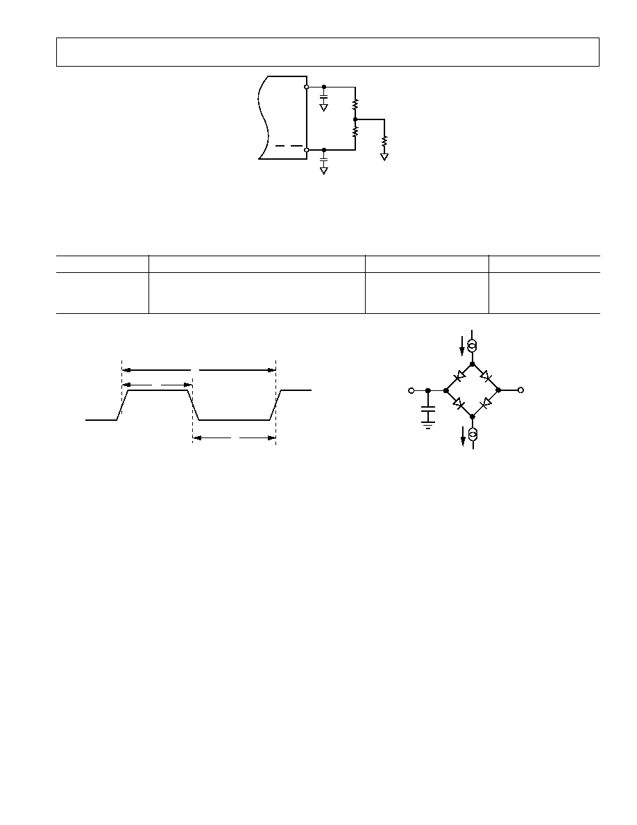
20k
20k
20pF
20pF
AD7011
ITx/QTx
ITx
/ QTx
40k
Figure 1. Analog Output Test Load Circuit
MASTER CLOCK TIMING
Parameter
Limit at T
A
= 40 C to +85 C
Units
Description
t
1
300
ns min
MCLK Cycle Time
t
2
100
ns min
MCLK High Time
t
3
100
ns min
MCLK Low Time
(V
AA
= V
DD
= +5 V 10%; AGND = DGND = 0 V. All specifications are T
MIN
to T
MAX
unless
otherwise noted.)
TO OUTPUT
PIN
+2.1V
I
OH
C
L
100pF
1.6mA
200µA
I
OL
Figure 3. Load Circuit for Digital Outputs
MCLK
t
2
t
1
t
3
Figure 2. Master Clock (MCLK) Timing
AD7011
REV. B
4
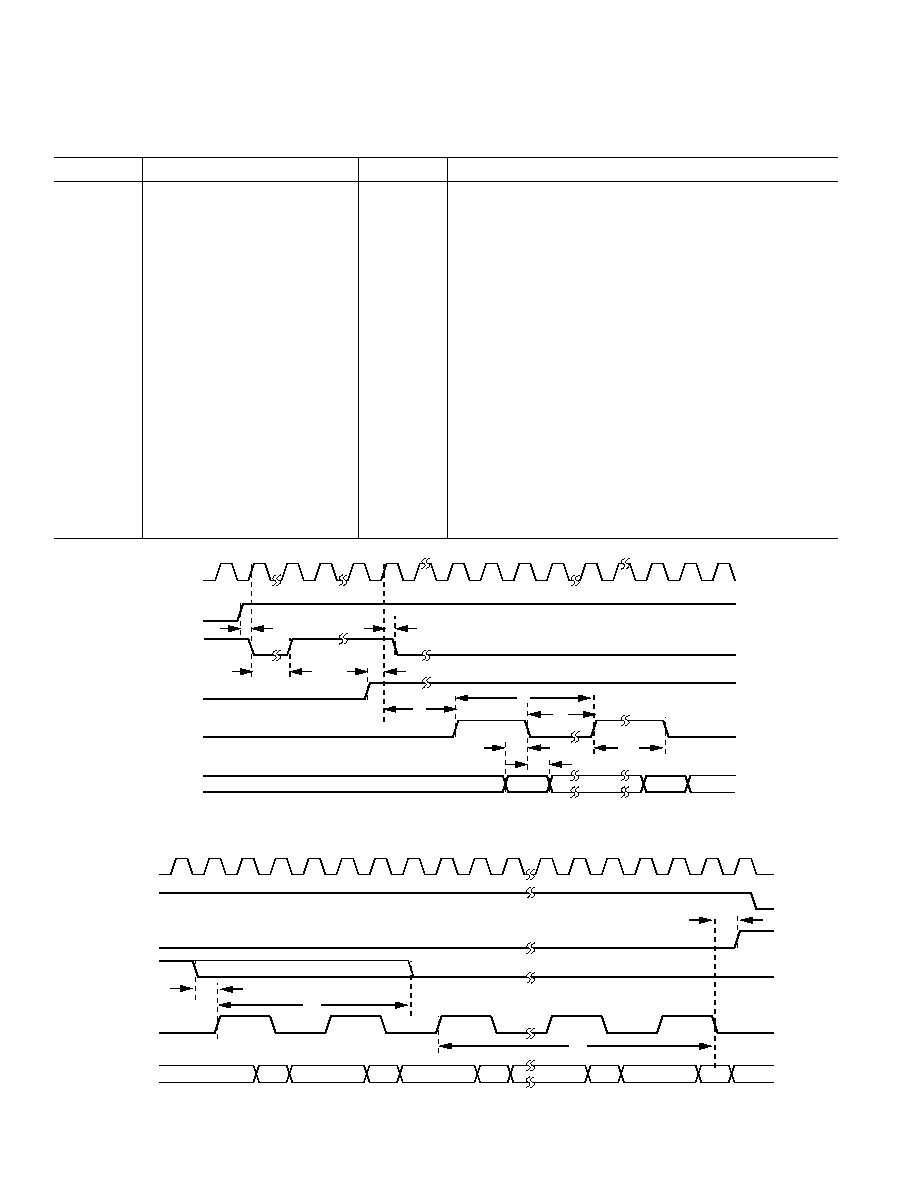
TRANSMIT SECTION TIMING
Parameter
Limit at T
A
= 40 C to +85 C
Units
Description
t
4
10
ns min
Power Setup Time.
t
1
10
ns max
t
5
4097t
1
+ 70
ns max
MCLK rising edge, after Power high, to READY rising edge.
t
6
10
ns min
BIN Setup Time.
t
1
10
ns max
t
7
t
1
+ 70
ns max
MCLK to READY propagation delay.
t
8
3t
1
+ 70
ns
MCLK rising edge, after BIN high, to first TxCLK rising edge.
t
9
64t
1
ns
TxCLK Cycle Time.
t
10
32t
1
ns
TxCLK High Time.
t
11
32t
1
ns
TxCLK Low Time.
t
12
50
ns min
TxCLK falling edge to TxDATA setup time.
t
13
0
ns min
TxCLK falling edge to TxDATA hold time.
t
14
3t
1
ns max
BIN low setup to Last transmitted symbol after ramp down.
t
15
124t
1
ns max
BIN low hold to Last transmitted symbol after ramp down.
t
16
7.5t
9
ns
Ramp Down cycle time after the last transmitted symbol.
t
17
30t
1
ns max
Last TxCLK falling edge to READY rising edge.
t
18
10
ns max
Digital Output Rise Time.
t
19
10
ns max
Digital Output Fall Time.
MCLK
READY
BIN
TxCLK
TxDATA
Y
k
t
4
t
5
t
7
t
9
t
10
t
11
t
12
t
13
t
8
t
6
X
k
POWER
Figure 4. Transmit Timing at the Start of a Tx Burst
MCLK
READY
BIN
TxCLK
TxDATA
t
14
X
N+4
Y
N+4
X
N+5
Y
N+8
X
N+8
t
17
POWER
t
15
t
16
Figure 5. Transmit Timing at the End of a Tx Burst
(V
AA
= V
DD
= +5 V 10%; AGND = DGND = 0 V, f
MCLK
= 3.1104 MHz. All specifications are
T
MIN
to T
MAX
unless otherwise noted.)
AD7011
REV. B
5
ANALOG MODE TIMING
Parameter
Limit at T
A
= 40
°
C to +85
°
C
Units
Description
t
20
15
ns min
MCLK Rising Edge to FRAME Setup Time.
t
21
15
ns min
MCLK Rising Edge to FRAME Hold Time.
15t
1
ns max
t
22
16t
1
ns
FRAME Cycle Time.
t
23
15
ns min
MCLK Rising Edge to Data Setup Time.
t
24
15
ns min
MCLK Rising Edge to Data Hold Time.
(V
AA
= V
DD
= +5 V
10%. AGND = DGND = 0 V. All specifications are T
MIN
to T
MAX
unless
otherwise noted.)
MCLK
t
20
FRAME
I DATA
DB9
DB8
DB1
DB0
DB9
DB8
DB7
Q DATA
DB9
DB8
DB1
DB0
DB9
DB8
DB7
t
23
t
24
t
21
t
22
Figure 6. Analog Mode Serial Interface Timing
Q
I
MODULAR OUTPUT
DURING FTEST
Figure 7. Modulator State During FTEST
Table I.
MODE 1
MODE 2
Operation
0
0
Digital TIA Mode
1
0
Analog Mode
0
1
FTEST
1
1
Factory Test, Reserved
Table II.
Mode of Operation
MODE 1
MODE 2
MCLK
Digital Bit Rate
DAC Update Rate
Digital Mode
0
0
3.1104 MHz
48.6 kHz
N/A
Analog Mode
1
0
2.56 MHz
N/A
160 kHz
AD7011
REV. B
6
Junction Temperature . . . . . . . . . . . . . . . . . . . . . . . . +150
°
C
SSOP
JA
Thermal Impedance . . . . . . . . . . . . . . . . +122
°
C/W
Lead Temperature, Soldering
Vapor Phase (60 sec) . . . . . . . . . . . . . . . . . . . . . +215
°
C
Infrared (15 sec) . . . . . . . . . . . . . . . . . . . . . . . . . +220
°
C
*Stresses above those listed under "Absolute Maximum Ratings" may cause
permanent damage to the device. This is a stress rating only and functional
operation of the device at these or any other conditions above those listed in the
operational sections of this specification is not implied. Exposure to absolute
maximum rating conditions for extended periods may affect device reliability.
ABSOLUTE MAXIMUM RATINGS*
(T
A
= +25
°
C unless otherwise noted)
V
DD
Tx, V
DD
Rx to AGND . . . . . . . . . . . . . . . 0.3 V to +7 V
AGND to DGND . . . . . . . . . . . . . . . . . . . . 0.3 V to +0.3 V
Digital I/O Voltage to DGND . . . . . . . 0.3 V to V
DD
+ 0.3 V
Analog I/O Voltage to AGND . . . . . . . 0.3 V to V
DD
+ 0.3 V
Operating Temperature Range
Industrial (A Version) . . . . . . . . . . . . . . . 40
°
C to +85
°
C
Storage Temperature Range . . . . . . . . . . . 65
°
C to + 150
°
C
WARNING!
ESD SENSITIVE DEVICE
CAUTION
ESD (electrostatic discharge) sensitive device. Electrostatic charges as high as 4000 V readily
accumulate on the human body and test equipment and can discharge without detection.
Although this device features proprietary ESD protection circuitry, permanent damage may
occur on devices subjected to high energy electrostatic discharges. Therefore, proper ESD
precautions are recommended to avoid performance degradation or loss of functionality.
ORDERING GUIDE
Model
Temperature Range
Package Description
Package Option
AD7011ARS
40
°
C to +85
°
C
Shrink Small Outline Package
RS-24
SSOP PIN CONFIGURATION
POWER
BIN (QDATA)
TxCLK (FRAME)
TxDATA (IDATA)
V
DD
DGND
MCLK
MODE1
NC
BOUT
AGND
QTx
QTx
V
AA
AGND
ITx
ITx
AGND
BYPASS
1
2
3
7
24
23
22
18
8
9
10
17
16
15
11
12
14
13
4
5
21
20
6
19
TOP VIEW
(Not to Scale)
AD7011
NC
MODE2
READY
NC
NC
NC = NO CONNECT

AD7011
REV. B
7
PIN FUNCTION DESCRIPTION
SSOP Pin
Number
Mnemonic
Function
POWER SUPPLY
19
V
AA
Positive power supply for analog section.
5
V
DD
Positive power supply for digital section.
14, 18, 23
AGND
Analog ground for transmit section.
6
DGND
Digital ground for transmit section.
ANALOG SIGNAL AND REFERENCE
13
BYPASS
Reference decoupling output. A decoupling capacitor should be connected between this pin and AGND.
16, 17
ITx, ITx
Differential analog outputs for the I channel, representing true and complementary outputs of the I
waveform.
21, 20
QTx, QTx
Differential analog outputs for the Q channel, representing true and complementary outputs of the Q
waveform.
TRANSMIT INTERFACE AND CONTROL
7
MCLK
Master clock, digital input. When operating in Mode 0 (TIA Digital mode), this pin should be driven by a
3.1104 MHz CMOS compatible clock source in digital mode and by 2.56 MHz CMOS compatible clock
source for analog mode.
3
TxCLK
This is a dual function digital input/output. When operating in Mode 0 (TIA Digital mode), this pin is
(FRAME)
configured as a digital output, transmit clock. This may be used to clock in transmit data at 48.6 kHz. When
operating in Mode 1 (analog mode), this pin is configured as a digital input, FRAME. This is used to frame
the clocking in of 16-bit words when bypassing the
/4 DQPSK modulator and directly loading the I and Q
10-bit DACs.
4
TxDATA
This is a dual function digital input. When operating in Mode 0 (TIA Digital mode), this pin is used to
(IDATA)
clock in transmit data on the falling edge of TxCLK at a rate of 48.6 kHz. When operating in Mode 1
(Analog mode), I data is clocked in on the rising edge of MCLK. This data bypasses the
/4 DQPSK modu-
lator and is loaded into the 10-bit I DAC.
2
BIN (QDATA) This is a dual function digital input. When operating in Mode 0 (TIA Digital mode), this input is used to ini-
tiate the ramping up (BIN high) or down (BIN low) of the I and Q waveforms. When operating in Mode 1
(Analog mode), Q data is clocked in on the rising edge of MCLK. This data bypasses the
/4 DQPSK modu-
lator and is loaded into the 10-bit Q DAC.
24
BOUT
Burst Out, digital output. This is the BIN input delayed by the pipeline delay, both digital and analog, of the
AD7011. This can be used to turn on and off the RF amplifiers in synchronization with the I and Q waveforms.
1
POWER
Transmit sleep mode, digital input. When this goes low, the AD7011 goes into sleep mode, drawing minimal
current. When this pin goes high, the AD7011 is brought out of sleep mode and initiates a self-calibration
routine to eliminate the offset between ITx & ITx and the offset between QTx & QTx.
12
READY
Transmit ready, digital output. This output goes high once the self-calibration routine is complete.
9, 11
MODE1,
Mode control, digital inputs. These are used to enter the AD7011 into three different operating modes,
MODE2
see Table I.
8, 10, 15, 22
NC
No Connects. These pins are no connects and should not be used as routes for other circuit signals.
AD7011
REV. B
8
TERMINOLOGY
Error Vector Magnitude
This is a measure of the rms error vector introduced by the
AD7011 where signal error vector is defined as the rms devia-
tion of a transmitted symbol from its ideal position when filtered
by an Ideal RRC Receive filter, as illustrated in Figure 8.
Gain Matching Between Channels
The is the gain matching between the I and Q outputs, measured
when transmitting all zeros.
Offset Vector Magnitude
This is a measure of the offset vector introduced by the AD7011
as illustrated in Figure 8. The offset vector is calculated so as to
minimize the rms error vector for each of the constellation
points.
Output Signal Range and Different Output Range
The output signal range is the output voltage swing and dc bias
level for each of the analog outputs. The different output range
is the difference between ITx and ITx for the I channel and the
difference between QTx and QTx for the Q Channel.
IS-54 Spurious Power
This is the rms sum of the spurious power measured at multiples
of 30 kHz, in a root raised cosine window of
±
16.4 kHz, relative
to twice the rms power in a RRC window in the 0 to 16.4 kHz
band.
Signal Vector Magnitude
This is the radius of the IQ constellation diagram as illustrated
in Figure 8.
Signal to (Noise + Distortion) Ratio
This is the measured ratio of signal to (noise + distortion) at the
output of the transmit I and Q DACs. The signal is the rms
amplitude of the fundamental. Noise is the rms sum of all non-
fundamental signals up to half the sampling frequency (f
S
/2),
excluding dc. The ratio is dependent upon the number of
quantization levels in the digitization process; the more levels,
the smaller the quantization noise. The theoretical signal to
(noise distortion) ratio for a sine wave is given by:
SNR = (6.02N + 1.76) dB
where N is the number of bits. Thus for an ideal 10-bit con-
verter, SNR = 61.96 dB.
I
Q
ERROR VECTOR
OFFSET
VECTOR
0,0
SIGNAL VECTOR
Figure 8.
AD7011
REV. B
9
I
Q
Figure 10.
/4 DQPSK Constellation Diagram
Figure 10 illustrates the
/4 DQPSK constellation diagram as
described above, showing the eight possible states for [I
k
, Q
k
].
The I
k
and Q
k
impulses are then filtered by FIR raised root
cosine filters (
= 0.35), generating 10-bit I and Q data. The
FIR root raised cosine filters have an impulse response of
±
4
symbols.
Transmit Calibration
When the transmit section is brought out of sleep mode
(POWER high), the transmit section initiates a self-calibration
routine to remove the offset between ITx and ITx and an offset
between QTx and QTx. READY goes high on the completion
of the self-calibration routine. Once READY goes high, BIN
(Burst In) can be brought high to initiate a transmit burst.
Ramp-Up/Down Envelope Logic
The AD7011 provides on-chip envelope shaping logic, providing
power shaping control for the beginning and end of a transmit
burst. When BIN (Burst In) is brought high, the modulator is
reset to a transmitting all zeros state (i.e., X
k
= Y
k
= 0) and
continues to transmit all zeros for the first three symbols, during
which the ramp-up envelope goes from zero to full scale as
illustrated in Figure 11. The next symbol to be transmitted is
[I
1
, Q
1
], which represents the first two data bits clocked in after
BIN going high, i.e., [X
1
, Y
1
].
COS
1
2
1
2
t
3T
+ COS
1
2
1
2
t
3T
3 SYMBOLS
3 SYMBOLS
Figure 11. Ramp Envelope
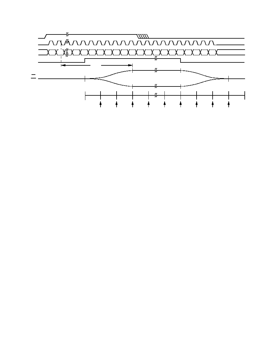
When BIN is brought low, indicating the end of a transmit
burst, the current Di-bit symbol [X
N+4
, Y
N+4
] that the AD7011
is receiving will be the last symbol to be computed for the four
symbol ramp-down sequence. Also the N
th
symbol is the last
active symbol prior to ramping down.
However, because the impulse response is equal to
±
4 symbols,
four additional symbols are required to fully compute the analog
outputs when transmitting the (N+4)
th
symbol. Hence there will
be eight subsequent TxCLKs, latching four additional Di-bit
symbols: [X
N + 5
, Y
N + 5
] to [X
N + 8
, Y
N + 8
].
CIRCUIT DESCRIPTION
TRANSMIT SECTION
The transmit section of the AD7011 generates
/4 DQPSK I
and Q waveforms in accordance with TIA specification. This is
accomplished by a digital
/4 DQPSK modulator, which
includes the root-raised cosine filters (
= 0.35), followed by
two 10-bit DACs and on-chip reconstruction filters. The
/4
DQPSK (Differential Quadrature Phase Shift Keying) digital
modulator generates 10-bit I and Q data in response to the
transmit data stream. The 10-bit I and Q DACs are filtered by
on-chip reconstruction filters, which also generate differential
analog outputs for both I and Q channels.
The AD7011 transmit channel also provides an analog mode,
where direct access to the I and Q DACs is provided, bypassing
the
/4 DQPSK modulator. This is provided so that the
AD7011 transmit channel can also be used to perform the
conversion and filtering of the analog waveforms required to
emulate the existing analog cellular system.
/4 DQPSK Modulator
The
/4 DQPSK modulator generates 10-bit I and Q data
(Inphase and Quadrature) which are loaded into the I and Q
10-bit transmit DACs.
Figure 9 shows the functional block diagram of the
/4 DQPSK
modulator. The transmit serial data (TxDATA) is first con-
verted into Di-bit symbols [X
k
, Y
k
], using a 2-bit serial to parallel
converter. The data is then differentially encoded; symbols are
transmitted as changes in phase rather than absolute phases.
Each symbol represents a phase change, as illustrated in Table
III, and this along with the previously transmitted symbol
determines the next symbol to be transmitted. The differential
phase encoder generates I and Q impulses [I
k
, Q
k
] in response to
the Di-bit symbols according to:
I
k
= COS [
k1
+
k
]
Q
k
= SIN [
k1
+
k
]
DIFFERENTIAL
PHASE
ENCODER
ROOT-RAISED
COSINE FILTER
I DATA
Q DATA
10
10
2-BIT
SERIAL TO
PARALLEL
CONVERTER
/4 DQPSK DIGITAL
MODULATOR
X
k
Y
k
I
k
Q
k
ROOT-RAISED
COSINE FILTER
TxDATA
Figure 9.
/4 DQPSK Modulator Functional Block Diagram
Table III.
X
k
Y
k
k
1
1
-
3
4
0
1
3
4
0
0
4
1
0
-
4
AD7011
REV. B
10
As Figure 12 illustrates, the ramp-down envelope reaches zero
after three symbols, hence the fourth symbol does not actually
get transmitted.
Reconstruction Filters
The reconstruction filters smooth the DAC output signals,
providing continuous time I and Q waveforms at the output
pins. These are 4th order Bessel low-pass filters with a 3 dB
frequency of approximately 25 kHz. The filters are designed to
have a linear phase response in the passband and due to the
reconstruction filters being on-chip, the phase mismatch
between the I and Q transmit channels is kept to a minimum.
Transmit Section Digital Interface
MODE1 = MODE2 = DGND: Digital
/4 DQPSK Mode
Figures 4 and 5 shows the timing diagrams for the transmit
interface when operating in TIA
/4 DQPSK mode. POWER is
sampled on the rising edge of MCLK. When POWER is
brought high, the transmit section is brought out of sleep mode
and initiates a self-calibration routine as described above. Once
the self-calibration is complete, the READY signal goes high to
indicate that a transmit burst can now begin. BIN (Burst in) is
brought high to initiate a transmit burst and should only be
brought high if the READY signal is already high.
When BIN goes high, the READY signal goes low on the next
rising edge of MCLK and TxCLK becomes active after a
further three MCLK cycles. TxCLK can be used to clock out
the transmit data from the ASIC or DSP on the rising edge of
TxCLK and the AD7011 will latch TxDATA on the falling
edge of TxCLK.
When BIN is brought low, the AD7011 will continue to clock in
the current Di-bit symbol (X
N + 4
, Y
N + 4
) and will continue for a
further 8 TxCLK cycles (four symbols). After the final TxCLK,
READY goes high waiting for BIN to be brought high to begin
the next transmit burst.
X
1
X
N
Y
N
Y
N+1
X
N+1
Y
N+2
X
N+2
Y
N+3
X
N+3
Y
N+4
X
N+4
3 SYMBOL
RAMP-UP ENVELOPE
3 SYMBOL
RAMP-DOWN ENVELOPE
I
1
Q
1
I
N
Q
N
I
N+1
Q
N+1
I
N+2
Q
N+2
I
N+3
Q
N+3
I
N+4
Q
N+4
0
0
0
0
SYMBOL
PHASE MAX
EFFECT
= 480
t
1
BIN
TxCLK
TxDATA
BOUT
(ITxITx),
(QTxQTx)
Y
N+5
X
N+5
Y
N+6
X
N+6
Y
N+7
X
N+7
Y
N+8
X
N+8
0
0
Y
1
Figure 12. Transmit Burst
When POWER is brought low this puts the transmit section into
a low power sleep mode, drawing minimal current. The analog
outputs go high impedance while in low power sleep mode.
MODE1 = V
DD
; MODE2 = DGND: Analog Mode
Figure 6 shows the timing diagram for the transmit interface
when operating in analog mode. In this mode the
/4 DQPSK
modulator is bypassed and direct access to the I and Q 10-bit
DACs is provided. Loading of the I and Q DACs is accom-
plished using a 4 wire 16-bit serial interface. The pins TxCLK,
TxDATA and BIN are all reconfigured as inputs, with the
functions of FRAME, IDATA and QDATA respectively.
I and Q data are loaded via the IDATA and QDATA pins and
FRAME synchronizes the loading of the 16-bit I and Q words.
FRAME should be brought high one clock cycle prior to the I
and Q MSBs. Data is latched on the rising edge of MCLK,
MSB first, where only the first 10 data bits are significant. Con-
tinuous updating of the I and Q DACs is required at a rate of
MCLK/16.
MODE1 = DGND; MODE2 = V
DD
: Frequency Test Mode
A special FTEST (Frequency TEST) mode is provided for the
customer, where no phase modulation takes place and the mod-
ulator outputs remain static. ITx is set to zero and QTx is set to
full scale as Figure 7 illustrates. However, the normal ramp-up/
down envelope is still applied during the beginning and end of a
burst.
MODE1 = MODE2 = V
DD
: Factory Test Mode
This mode is reserved for factory test only and should not be
used by the customer for correct device operation.
AD7011
REV. B
11
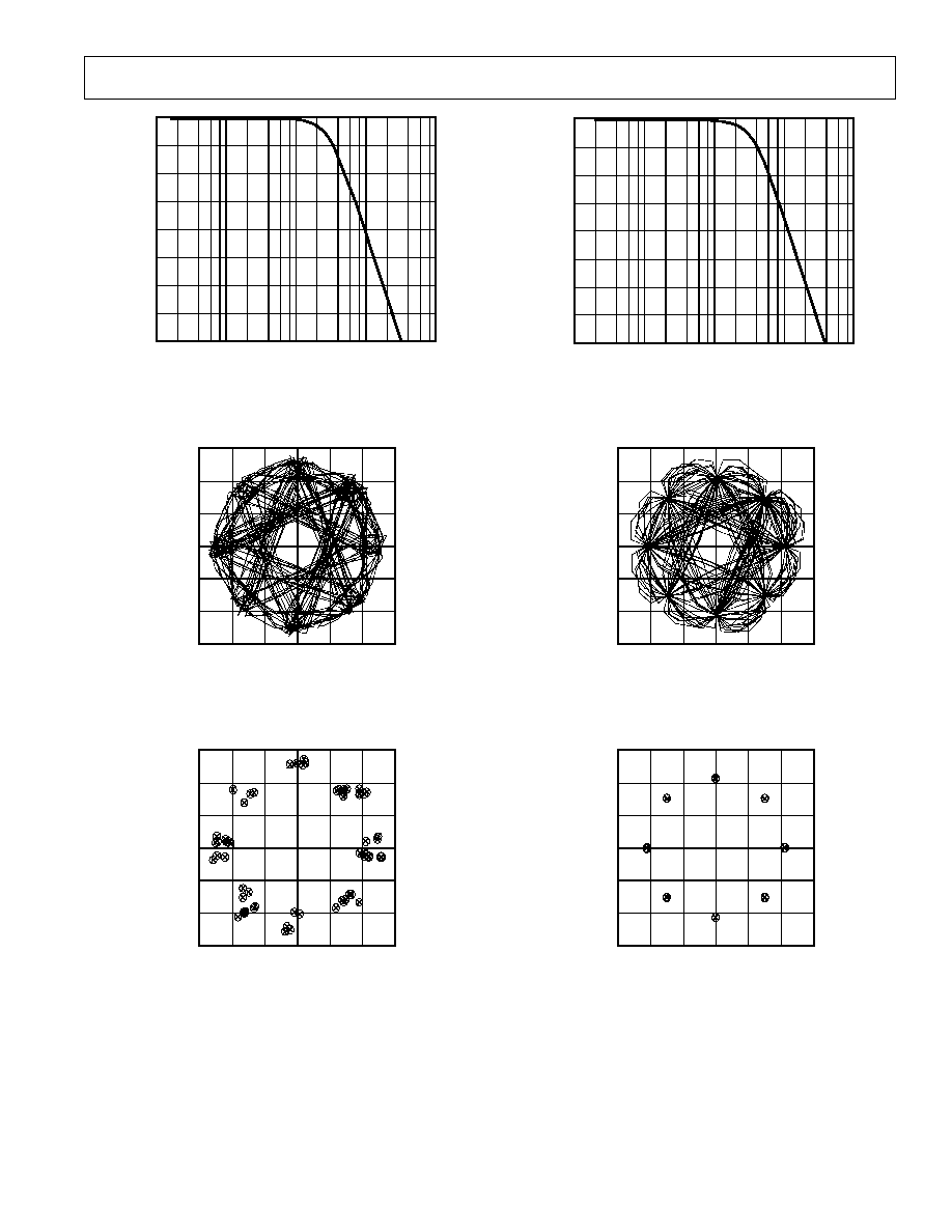
0
40
80
1
1000
100
10
0.1
60
20
30
50
70
10
FREQUENCY kHz
MAGNITUDE dBs
Figure 13. Reconstruction Filter Frequency Response for
the I and Q DACs, MCLK = 2.56 MHz
I Channel Volts
Q Channel Volts
1.2
1.2
1.2
0
0.8
0.8
0.4
1.2
0.8
0.4
0.8
0.4
0
0.4
I Channel Volts
Q Channel Volts
1.2
1.2
1.2
0
0.8
0.8
0.4
1.2
0.8
0.4
0.8
0.4
0
0.4
Figure 14. AD7011 I vs. Q Waveforms When Transmitting
Random Data
I Channel Volts
Q Channel Volts
1.2
1.2
1.2
0
0.8
0.8
0.4
1.2
0.8
0.4
0.8
0.4
0
0.4
Figure 15. AD7011 Transmit Constellation Diagram
0
40
80
1
1000
100
10
0.1
60
20
30
50
70
10
FREQUENCY kHz
MAGNITUDE dBs
Figure 16. Reconstruction Filter Frequency Response for
the I and Q DACs, MCLK = 3.1104 MHz
I Channel Volts
Q Channel Volts
1.2
1.2
1.2
0
0.8
0.8
0.4
1.2
0.8
0.4
0.8
0.4
0
0.4
Figure 17. AD7011 I vs. Q Waveforms Filtered by an Ideal
Root Raised Cosine Receive Filter
I Channel Volts
Q Channel Volts
1.2
1.2
1.2
0
0.8
0.8
0.4
1.2
0.8
0.4
0.8
0.4
0
0.4
Figure 18. AD7011 Constellation Diagram When Filtered
by an Ideal Root Raised Cosine Receive Filter
AD7011
REV. B
12
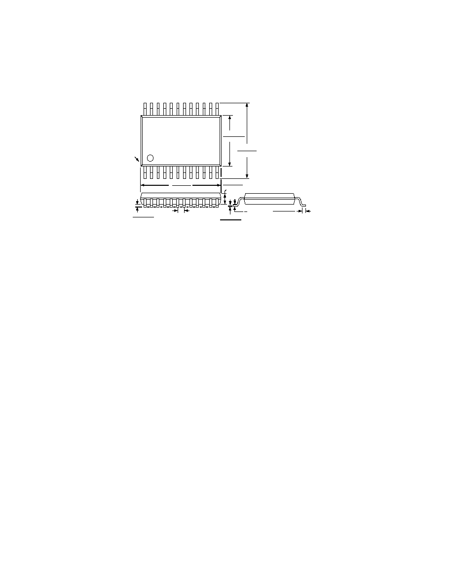
OUTLINE DIMENSIONS
Dimensions shown in inches and (mm).
C1780a57/94
PRINTED IN U.S.A.
24-Lead SSOP (RS-24)
1. LEAD NO. 1 IDENTIFIED BY A DOT.
2. LEADS WILL BE EITHER TIN PLATED OR SOLDER DIPPED
IN ACCORDANCE WITH MIL-M-38510 REQUIREMENTS
0.009 (0.229)
0.005 (0.127)
0.037 (0.94)
0.022 (0.559)
8°
0°
0.0256 (0.65)
BSC
0.07 (1.78)
0.066 (1.67)
0.328 (8.33)
0.318 (8.08)
0.008 (0.203)
0.002 (0.050)
PIN 1
0.311 (7.9)
0.301 (7.64)
0.212 (5.38)
0.205 (5.207)
1
24
13
12