 | ÐлекÑÑоннÑй компоненÑ: AD707AQ | СкаÑаÑÑ:  PDF PDF  ZIP ZIP |
Äîêóìåíòàöèÿ è îïèñàíèÿ www.docs.chipfind.ru
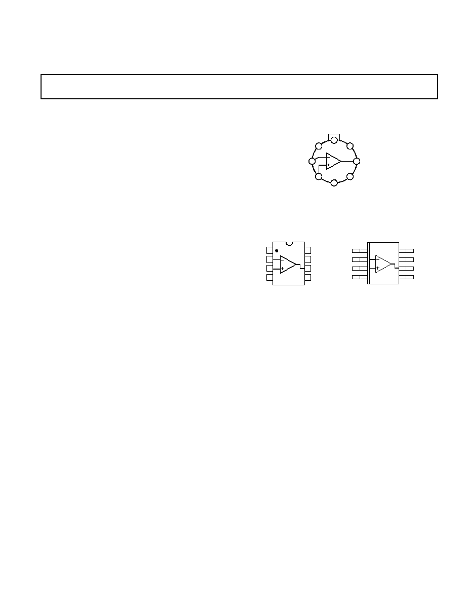
CONNECTION DIAGRAMS
TO-99 (H) Package
AD707
7
6
2
8
1
3
4
5
NULL
NULL
IN
+IN
V
S
+V
S
OUTPUT
NC
NC = NO CONNECT
NOTE: PIN 4 CONNECTED
TO CASE
Plastic (N) and
Cerdip (Q) Packages SOIC (R) Package
REV. B
Information furnished by Analog Devices is believed to be accurate and
reliable. However, no responsibility is assumed by Analog Devices for its
use, nor for any infringements of patents or other rights of third parties
which may result from its use. No license is granted by implication or
otherwise under any patent or patent rights of Analog Devices.
a
Ultralow Drift Op Amp
AD707
© Analog Devices, Inc., 1995
One Technology Way, P.O. Box 9106, Norwood, MA 02062-9106, U.S.A.
Tel: 617/329-4700
Fax: 617/326-8703
FEATURES
Very High DC Precision
15 V max Offset Voltage
0.1 V/ C max Offset Voltage Drift
0.35 V p-p max Voltage Noise (0.1 Hz to 10 Hz}
8 V/ V min Open-Loop Gain
130 dB min CMRR
120 dB min PSRR
1 nA max Input Bias Current
AC Performance
0.3 V/ s Slew Rate
0.9 MHz Closed-Loop Bandwidth
Dual Version: AD708
Available in Tape and Reel in Accordance with
EIA-481A Standard
APPLICATION HIGHLIGHTS
1. The AD707's 13 V/
µ
V typical open-loop gain and 140 dB
typical common-mode rejection ratio make it ideal for
precision instrumentation applications.
2. The precision of the AD707 makes tighter error budgets
possible at a lower cost.
3. The low offset voltage drift and low noise of the AD707 allow
the designer to amplify very small signals without sacrificing
overall system performance.
4. The AD707 can be used where chopper amplifiers are
required, but without the inherent noise and application
problems.
5. The AD707 is an improved pin-for-pin replacement for the
LT1001.
PRODUCT DESCRIPTION
The AD707 is a low cost, high precision op amp with state-of-
the-art performance that makes it ideal for a wide range of
precision applications. The offset voltage spec of less than 15
µ
V
is the best available in a bipolar op amp, and maximum input
offset current is 1.0 nA. The top grade is the first bipolar
monolithic op amp to offer a maximum offset voltage drift of
0.1
µ
V/
°
C, and offset current drift and input bias current drift
are both specified at 25 pA/
°
C maximum.
The AD707's open-loop gain is 8 V/
µ
V minimum over the full
±
10 V output range when driving a 1 k
load. Maximum input
voltage noise is 350 nV p-p (0.1 Hz to 10 Hz). CMRR and
PSRR are 130 dB and 120 dB minimum, respectively.
The AD707 is available in versions specified over commercial,
industrial and military temperature ranges. It is offered in 8-pin
plastic mini-DIP, small outline (SOIC), hermetic cerdip and
hermetic TO-99 metal can packages. Chips, MIL-STD-883B,
Rev. C, and tape & reel parts are also available.
1
2
3
4
8
7
6
5
AD707
NC = NO CONNECT
NULL
NC
OUTPUT
+V
S
NULL
IN
+IN
V
S
AD707
1
4
8
5
NC = NO CONNECT
NULL
NC
OUTPUT
+V
S
NULL
IN
+IN
V
S

AD707SPECIFICATIONS
REV. B
2
(@ +25 C and 15 V, unless otherwise noted)
AD707J/A
AD707K/B
Conditions
Min
Typ
Max
Min
Typ
Max
Units
INPUT OFFSET VOLTAGE
Initial
30
90
10
25
µ
V
vs. Temperature
0.3
1.0
0.1
0.3
µ
V/
°
C
T
MIN
to T
MAX
50
100
15
45
µ
V
Long-Term Stability
0.3
0.3
µ
V/month
Adjustment Range
R2 = 20 k
(Figure 19)
±
4
±
4
mV
INPUT BIAS CURRENT
1.0
2.5
0.5
2.0
nA
T
MIN
to T
MAX
2.0
4.0
1.5
4.0
nA
Average Drift
15
40
15
40/40/40
pA/
°
C
OFFSET CURRENT
V
CM
= 0 V
0.5
2.0
0.3
1.5
nA
T
MIN
to T
MAX
2.0
4.0
1.0
2.0
nA
Average Drift
2
40
1
25/25/35
pA/
°
C
INPUT VOLTAGE NOISE
0.1 Hz to 10 Hz
0.23
0.6
0.23
0.6
µ
V p-p
f = 10 Hz
10.3
28
10.3
18
nV/
Hz
f = 100 Hz
10.0
13.0
10.0
12
nV/
Hz
f = 1 kHz
9.6
11.0
9.6
11.0
nV/
Hz
INPUT CURRENT NOISE
0.1 Hz to 10 Hz
14
35
14
30
pA p-p
f = 10 Hz
0.32
0.9
0.32
0.8
pA/
Hz
f = 100 Hz
0.14
0.27
0.14
0.23
pA/
Hz
f = 1 kHz
0.12
0.18
0.12
0.17
pA/
Hz
COMMON-MODE
REJECTION RATIO
V
CM
=
±
13 V
120
140
130
140
dB
T
MIN
to T
MAX
120
140
120
140
dB
OPEN-LOOP GAIN
V
O
=
±
10 V
R
LOAD
2 k
3
13
5
13
V/
µ
V
T
MIN
to T
MAX
3
13
3
13
V/
µ
V
POWER SUPPLY
REJECTION RATIO
V
S
=
±
3 V to
±
18 V
110
130
115
130
dB
T
MIN
to T
MAX
110
130
110
130
dB
FREQUENCY RESPONSE
Closed-Loop Bandwidth
0.4
0.9
0.4
0.9
MHz
Slew Rate
0.12
0.3
0.12
0.3
V/
µ
s
INPUT RESISTANCE
Differential
24
100
45
200
M
Common Mode
200
300
G
OUTPUT CHARACTERISTICS
Voltage
R
LOAD
10 k
13.5
14
13.5
14
±
V
R
LOAD
2 k
12.5
13.0
12.5
13.0
±
V
R
LOAD
1 k
12.0
12.5
12.0
12.5
±
V
R
LOAD
2 k
T
MIN
to T
MAX
12.0
13.0
12.0
13.0
±
V
OPEN-LOOP OUTPUT
RESISTANCE
60
60
POWER SUPPLY
Current, Quiescent
2.5
3
2.5
3
mA
Power Consumption, No Load
V
S
=
±
15 V
75
90
75
90
mW
V
S
=
±
3 V
7.5
9.0
7.5
9.0
mW
NOTES
All min and max specifications are guaranteed. Specifications in boldface are tested on all production units at final electrical test. Results from those tests are used to
calculate outgoing quality levels.
Specifications subject to change without notice.
AD707
REV. B
3
ABSOLUTE MAXIMUM RATINGS
1
Supply Voltage . . . . . . . . . . . . . . . . . . . . . . . . . . . . . . .
±
22 V
Internal Power Dissipation
2
. . . . . . . . . . . . . . . . . . . . 500 mW
Input Voltage . . . . . . . . . . . . . . . . . . . . . . . . . . . . . . . . . .
±
V
S
Output Short Circuit Duration . . . . . . . . . . . . . . . . Indefinite
Differential Input Voltage . . . . . . . . . . . . . . . . . +V
S
and V
S
Storage Temperature Range (Q, H) . . . . . . 65
°
C to +150
°
C
Storage Temperature Range (N, R) . . . . . . . 65
°
C to +125
°
C
Lead Temperature Range (Soldering 60 sec) . . . . . . . +300
°
C
NOTES
1
Stresses above those listed under "Absolute Maximum Ratings" may cause
permanent damage to the device. Exposure to absolute maximum rating condi-
tions for extended periods may affect device reliability.
2
8-pin plastic package:
JA
= 165
°
C/Watt; 8-pin cerdip package:
JA
= 110
°
C/Watt;
8-pin small outline package:
JA
= 155
°
C/Watt; 8-pin header package:
JA
=
200
°
C/Watt.
ORDERING GUIDE
Temperature
Package
Package
Model
Range
Description
Option
AD707AH
40
°
C to +85
°
C
8-Pin Metal Can
H-08A
AD707AQ
40
°
C to +85
°
C
8-Pin Ceramic DIP
Q-8
AD707AR
40
°
C to +85
°
C
8-Pin Plastic SOIC
SO-8
AD707AR-REEL
40
°
C to +85
°
C
8-Pin Plastic SOIC
SO-8
AD707AR-REEL7
40
°
C to +85
°
C
8-Pin Plastic SOIC
SO-8
AD707BQ
40
°
C to +85
°
C
8-Pin Ceramic DIP
Q-8
AD707JN
0
°
C to +70
°
C
8-Pin Plastic DIP
N-8
AD707JR
0
°
C to +70
°
C
8-Pin Plastic SOIC
SO-8
AD707JR-REEL
0
°
C to +70
°
C
8-Pin Plastic SOIC
SO-8
AD707JR-REEL7
0
°
C to +70
°
C
8-Pin Plastic SOIC
SO-8
AD707KN
0
°
C to +70
°
C
8-Pin Plastic DIP
N-8
AD707KR
0
°
C to +70
°
C
8-Pin Plastic SOIC
SO-8
AD707KR-REEL
0
°
C to +70
°
C
8-Pin Plastic SOIC
SO-8
AD707KR-REEL7
0
°
C to +70
°
C
8-Pin Plastic SOIC
SO-8
METALIZATION PHOTOGRAPH
Dimensions shown in inches and (mm).
Contact factory for latest dimensions.
0.059
(1.51)
NULL
8
+V
S
7
6
V
OUT
4
V
S
3
+IN
2
IN
1
NULL
0.110 (2.79)
WARNING!
ESD SENSITIVE DEVICE
CAUTION
ESD (electrostatic discharge) sensitive device. Electrostatic charges as high as 4000 V readily
accumulate on the human body and test equipment and can discharge without detection.
Although the AD707 features proprietary ESD protection circuitry, permanent damage may
occur on devices subjected to high energy electrostatic discharges. Therefore, proper ESD
precautions are recommended to avoid performance degradation or loss of functionality.
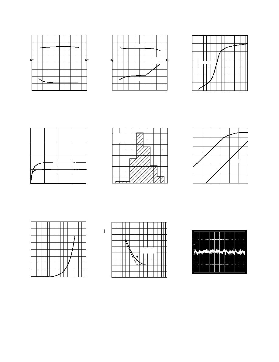
AD707Typical Characteristics
REV. B
4
SUPPLY VOLTAGE
±
V
+V
S
1.5
V
S
0
25
5
10
15
20
0.5
1.0
+1.5
+0.5
+1.0
+ V
OUT
V
OUT
OUTPUT VOLTAGE SWING
±
V
(REFERRED TO SUPPLY VOLTAGES)
R
L
= 2k
@ +25
°
C
Figure 2. Output Voltage Swing
vs. Supply Voltage
OFFSET VOLTAGE DRIFT µV/
°
C
NUMBER OF UNITS
100
70
20
0.4 0.3
0.4
0.2 0.1
0
0.1
0.2
0.3
90
80
50
30
60
40
10
0
256 UNITS
TESTED
55
°
C TO +125
°
C
Figure 5. Typical Distribution of
Offset Voltage Drift
FREQUENCY Hz
45
40
0
0.01
0.1
100
1
10
35
30
25
20
15
10
5
INPUT VOLTAGE NOISE nV/
Hz
I/F CORNER
0.7Hz
Figure 8. Input Noise Spectral
Density
LOAD RESISTANCE
OUTPUT VOLTAGE V p -p
35
15
0
10
100
10k
1k
10
25
20
30
5
±
15V SUPPLIES
Figure 3. Output Voltage Swing
vs. Load Resistance
FREQUENCY Hz
OUTPUT IMPEDANCE
100
0.0001
0.1
100k
1
10
100
1k
10k
10
1
0.1
0.001
0.01
I
O
= 1mA
A
V
= +1000
A
V
= +1
Figure 6. Output Impedance vs.
Frequency
10
0%
100
90
TIME 1sec/Div
VOLTAGE NOISE 100nV/Div
Figure 9. 0.1 Hz to 10 Hz Voltage
Noise
SUPPLY VOLTAGE
±
V
+V
S
1.5
0.5
1.0
V
S
+1.5
+0.5
+1.0
0
25
5
10
15
20
+V
V
COMMOM-MODE VOLTAGE LIMIT V
(REFERRED TO SUPPLY VOLTAGES)
Figure 1. Input Common-Mode
Range vs. Supply Voltage
TIME AFTER POWER ON Minutes
CHANGE IN OFFSET µV
4
0
0
4
1
2
3
3
2
1
DUAL-IN-LINE PACKAGE
PLASTIC (N) or CERDIP (Q)
METAL CAN (H) PACKAGE
Figure 4. Offset Voltage Warm-Up
Drift
DIFFERENTIAL VOLTAGE
±
V
40
30
0
0
1
100
10
20
10
INVERTING OR
NONINVERTING INPUT CURRENT mA
Figure 7. Input Current vs.
Differential Input Voltage
AD707
REV. B
5
TEMPERATURE
°
C
16
10
0
60 40
140
20
0
20
40
60
80 100 120
14
12
6
2
8
4
OPEN-LOOP GAIN
V/µV
R
L
=
1k
V
OUT
=
±
10V
Figure 10. Open-Loop Gain vs.
Temperature
FREQUENCY Hz
COMMON-MODE REJECTION dB
160
0
0.1
1
10
100
1k
10k
100k
1M
140
100
80
60
20
120
40
Figure 13. Common-Mode
Rejection vs. Frequency
SUPPLY VOLTAGE
±
V
SUPPLY CURRENT mA
4
0
0
3
24
6
9
12
15
18
21
2
1
3
+125
°
C
+25
°
C
55
°
C
Figure 16. Supply Current vs.
Supply Voltage
SUPPLY VOLTAGE V
OPEN-LOOP GAIN
V/µV
16
10
0
0
25
5
10
15
20
14
12
6
2
8
4
R
LOAD
= 1k
Figure 11. Open-Loop Gain vs.
Supply Voltage
FREQUENCY Hz
OUTPUT VOLTAGE V p-p
35
15
0
1k
10k
1M
100k
10
25
20
30
5
F
MAX
= 3kHz
R
L
= 2k
+25
°
C
V
S
=
±
15V
Figure 14. Large Signal Frequency
Response
20mV/DIV
CH1
TIME 2µs/DIV
Figure 17. Small Signal Transient
Response; A
V
= +1, R
L
= 2 k
,
C
L
= 50 pF
FREQUENCY Hz
OPEN-LOOP GAIN
V/µV
140
80
0
0.01 0.1
1
10 100 1k 10k 100k 1M 10M
120
100
40
10
60
20
PHASE Degrees
30
180
0
90
150
60
120
R
L
= 2k
C
L
= 1000pF
PHASE
MARGIN
=58
°
GAIN
Figure 12. Open-Loop Gain and
Phase vs. Frequency
FREQUENCY Hz
POWER SUPPLY REJECTION dB
160
0
0.001 0.01
100k
0.1
1
10
100
1k
10k
140
80
60
40
20
120
100
Figure 15. Power Supply Rejection
vs. Frequency
20mV/DIV
CH1
TIME 2µs/DIV
Figure 18. Small Signal Transient
Response; A
V
= +1, R
L
= 2 k
,
C
L
= 1000 pF
AD707
REV. B
6
OPERATION WITH A GAIN OF 100
Demonstrating the outstanding dc precision of the AD707 in
practical applications, Table I shows an error budget calculation
for the gain of 100 configuration shown in Figure 21.
Table I. Error Budget
Maximum Error Contribution
Av = 100 (C Grade)
Error Source
(Full Scale: V
OUT
= 10 V, V
IN
= 100 mV)
V
OS
15
µ
V/100 mV
= 150 ppm
I
OS
(100
)(1 nA)/100 mV
=
1 ppm
Gain (2 k
Load) (100 V/8
×
10
6
)100 mV
= 13 ppm
Noise
0.35
µ
V/100 mV
=
4 ppm
V
OS
Drift
(0.1 V/
°
C)/100 mV
=
1 ppm/
°
C
= 168 ppm
+1 ppm/
°
C
Total Unadjusted Error
@ +25
°
C
= 168 ppm > 12 Bits
@ 55
°
C to +125
°
C
= 268 ppm > 11 Bits
With Offset Calibrated Out
@ +25
°
C
= 17 ppm > 15 Bits
@ 55
°
C to +125
°
C
= 117 ppm > 13 Bits
6
2
3
+V
S
AD707
0.1µF
V
S
4
99
V
OUT
0.1µF
7
V
IN
10k
100
Figure 21. Gain of 100 Configuration
Although the initial offset voltage of the AD707 is very low, it is
nonetheless the major contributor to system error. In cases
requiring additional accuracy, the circuit shown in Figure 19
can be used to null out the initial offset voltage. This method
will also cancel the effects of input offset current error. With the
offsets nulled, the AD707C will add less than 17 ppm of error.
This error budget assumes no error in the resistor ratio and no
errors from power supply variation (the 120 dB minimum PSRR
of the AD707C makes this a good assumption). The external
resistors can cause gain error from mismatch and drift over
temperature.
OFFSET NULLING
The input offset voltage of the AD707 is the lowest available in
a bipolar op amp, but if additional nulling is required, the
circuit shown in Figure 19 offers a null range of 200
µ
V. For
wider null capability, omit R1 and substitute a 20 k
potenti-
ometer for R2.
6
2
3
8
R2
2k
1
R1
10k
0.1µF
+V
S
7
AD707
0.1µF
V
S
4
OFFSET
ADJUST
Figure 19. External Offset Nulling and Power Supply
Bypassing
GAIN LINEARITY INTO A 1 k
LOAD
The gain and gain linearity of the AD707 are the highest
available among monolithic bipolar amplifiers. Unlike other dc
precision amplifiers, the AD707 shows no degradation in gain or
gain linearity when driving loads in excess of 1 k
over a
±
10 V
output swing. This means high gain accuracy is assured over the
output range. Figure 20 shows the gain of the AD707, OP07, and
the OP77 amplifiers when driving a 1 k
load.
The AD707 will drive 10 mA of output current with no signifi-
cant effect on its gain or linearity.
OUTPUT VOLTAGE V
CHANGE IN OFFSET VOLTAGE 10µV/Div
15
15
10
5
0
5
10
AD707
OP07
OP77
@ +25
°
C
R
LOAD
= 1k
Figure 20. Gain Linearity of the AD707 vs.
Other DC Precision Op Amps
AD707
REV. B
7
18-BIT SETTLING TIME
Figure 22 shows the AD707 settling to within 80
µ
V of its final
value for a 20 V output step in less than 100
µ
s (in the test con-
figuration shown in Figure 23). To achieve settling to 18 bits,
any amplifier specified to have a gain of 4 V/
µ
V would appear to
be good enough, however, this is not the case. In order to truly
achieve 18-bit accuracy, the gain linearity must be better than
4 ppm.
The gain nonlinearity of the AD707 does not contribute to the
error, and the gain itself only contributes 0.1 ppm. The gain
error, along with the V
OS
and V
OS
drift errors do not comprise
1 LSB of error in an 18-bit system over the military temperature
range. If calibration is used to null offset errors, the AD707
resolves up to 20 bits at +25
°
C.
TIME 50µs/Div
REFERENCE
SIGNAL
10V/Div
D.U.T.
OUTPUT
ERROR
50µV/Div
OUTPUT:
10V/Div
Figure 22. 18-Bit Settling
V
S
6
2
3
OP27
200k
2x HP1N6263
V
ERROR
x 100
7
10µF
0.1µF
+V
S
10µF
0.1µF
V
S
6
2
3
D.U.T.
AD707
100
7
10µF
0.1µF
+V
S
10µF
0.1µF
1.9k
2k
4
2k
V
IN
FLAT-TOP
PULSE
GENERATOR
DATA
DYNAMICS
5109
OR
EQUIVALENT
2k
4
Figure 23. Op Amp Settling Time Test Circuit
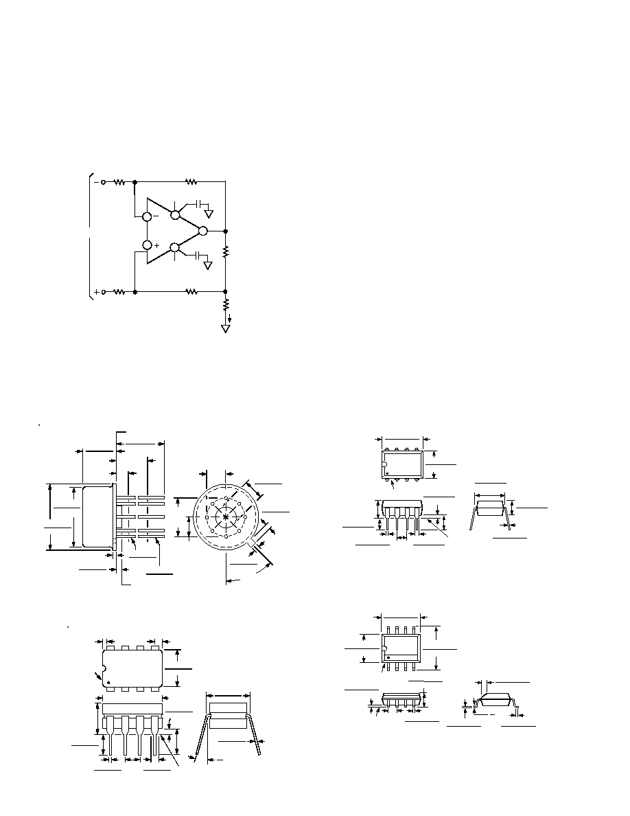
140 dB CMRR INSTRUMENTATION AMPLIFIER
The extremely tight dc specifications of the AD707 enable the
designer to build very high performance, high gain instrumenta-
tion amplifiers without having to select matched op amps for the
crucial first stage. For the second stage, the lowest grade AD707
is ideally suited. The CMRR is typically the same as the high
grade parts, but does not exact a premium for drift performance
(which is less critical in the second stage). Figure 24 shows an
example of the classic instrumentation amp. Figure 25 shows
that the circuit has at least 140 dB of common-mode rejection
for a
±
10 V common-mode input at a gain of 1001 (R
G
= 20
).
6
2
3
A1
AD707
10k
200
9.9k
R2
10k
IN
R4
10k
R
G
10k
R1
10k
6
2
3
A3
AD707
6
2
3
A2
AD707
+IN
R2
R
CM
CIRCUIT GAIN = + 1
R
G
20,000
Figure 24. A 3 Op Amp Instrumentation Amplifier
High CMRR is obtained by first adjusting R
CM
until the output
does not change as the input is swept through the full common-
mode range. The value of R
G
, should then be selected to achieve
the desired gain. Matched resistors should be used for the
output stage so that R
CM
is as small as possible. The smaller the
value Of R
CM
, the lower the noise introduced by potentiometer
wiper vibrations. To maintain the CMRR at 140 dB over a
20
°
C range, the resistor ratios in the output stage, R1/R2 and
R3/R4, must track each other better than 10 ppm/
°
C.
TIME 2 sec/Div
CH1
CH2
INPUT
COMMON-MODE
SIGNAL: 10V/Div
COMMON-MODE
ERROR REFERRED
TO INPUT: 5µV/Div
Figure 25. Instrumentation Amplifier
Common-Mode Rejection
AD707
REV. B
8
C1164a212/95
PRINTED IN U.S.A.
OUTLINE DIMENSIONS
Dimensions shown in inches and (mm).
8-Pin Metal Can
(H-08A)
45
°
BSC
0.100
(2.54)
BSC
0.034 (0.86)
0.027 (0.69)
0.045 (1.14)
0.027 (0.69)
0.160 (4.06)
0.110 (2.79)
0.100
(2.54)
BSC
0.200
(5.08)
BSC
6
8
5
7
1
4
2
3
REFERENCE PLANE
BASE & SEATING PLANE
0.335 (8.51)
0.305 (7.75)
0.370 (9.40)
0.335 (8.51)
0.750 (19.05)
0.500 (12.70)
0.045 (1.14)
0.010 (0.25)
0.050
(1.27)
MAX
0.040 (1.02) MAX
0.019 (0.48)
0.016 (0.41)
0.021 (0.53)
0.016 (0.41)
0.185 (4.70)
0.165 (4.19)
0.250 (6.35)
MIN
8-Pin Cerdip
(Q-8)
0.320 (8.13)
0.290 (7.37)
0.015 (0.38)
0.008 (0.20)
15
°
0
°
0.005 (0.13) MIN
0.055 (1.4) MAX
1
PIN 1
4
5
8
0.310 (7.87)
0.220 (5.59)
0.405 (10.29) MAX
0.200
(5.08)
MAX
SEATING
PLANE
0.023 (0.58)
0.014 (0.36)
0.070 (1.78)
0.030 (0.76)
0.060 (1.52)
0.015 (0.38)
0.150
(3.81)
MIN
0.200 (5.08)
0.125 (3.18)
0.100
(2.54)
BSC
8-Pin Plastic DIP
(N-8)
8
1
4
5
0.430 (10.92)
0.348 (8.84)
0.280 (7.11)
0.240 (6.10)
PIN 1
SEATING
PLANE
0.022 (0.558)
0.014 (0.356)
0.060 (1.52)
0.015 (0.38)
0.210 (5.33)
MAX
0.130
(3.30)
MIN
0.070 (1.77)
0.045 (1.15)
0.100
(2.54)
BSC
0.160 (4.06)
0.115 (2.93)
0.325 (8.25)
0.300 (7.62)
0.015 (0.381)
0.008 (0.204)
0.195 (4.95)
0.115 (2.93)
8-Lead SOIC
(SO-8)
0.1968 (5.00)
0.1890 (4.80)
8
5
4
1
0.2440 (6.20)
0.2284 (5.80)
PIN 1
0.1574 (4.00)
0.1497 (3.80)
0.0688 (1.75)
0.0532 (1.35)
SEATING
PLANE
0.0098 (0.25)
0.0040 (0.10)
0.0192 (0.49)
0.0138 (0.35)
0.0500
(1.27)
BSC
0.0098 (0.25)
0.0075 (0.19)
0.0500 (1.27)
0.0160 (0.41)
8
°
0
°
0.0196 (0.50)
0.0099 (0.25)
x 45
°
PRECISION CURRENT TRANSMITTER
The AD707's excellent dc performance, especially the low offset
voltage, low offset voltage drift and high CMRR, makes it
possible to make a high precision voltage-controlled current
transmitter using a variation of the Howland Current Source
circuit (Figure 26). This circuit provides a bidirectional load
current which is derived from a differential input voltage.
6
2
3
+V
S
AD707
0.1µF
V
S
4
0.1µF
7
R4
100k
R3
100k
R2
100k
R1
100k
R
L
I
L
R
SCALE
V
IN
V
IN
R
SCALE
t
L
=
( )
R2
R1
Figure 26. Precision Current Source/Sink
The performance and accuracy of this circuit will depend almost
entirely on the tolerance and selection of the resistors. The scale
resistor (R
SCALE
) and the four feedback resistors directly affect
the accuracy of the load current and should be chosen carefully
or trimmed.
As an example of the accuracy achievable, assume I
L
must be
10 mA, and the available V
IN
is only 10 mV.
R
SCALE
= 10 mV/10 mA = 1
I
ERROR
due to the AD707C:
Maximum I
ERROR
= 2(V
OS
)/R
SCALE
+ 2(V
OS
Drift)/R
SCALE
+
I
OS
(100 k/R
SCALE
)
= 2 (15
µ
V)/l
+2 (0.1
µ
V/
°
C)/l
+ 1 nA (100 k)/l
(1.5 nA @ 125
°
C)
= 30
µ
A + 0.2
µ
A/
°
C + 100
µ
A
(150
µ
A @ 125
°
C)
= 130
µ
A/10 mA = 1.3% @ 25
°
C
= 180
µ
A/10 mA = 1.8% @ 125
°
C
Low drift, high accuracy resistors are required to achieve high
precision.