 | –≠–ª–µ–∫—Ç—Ä–æ–Ω–Ω—ã–π –∫–æ–º–ø–æ–Ω–µ–Ω—Ç: AD7118L | –°–∫–∞—á–∞—Ç—å:  PDF PDF  ZIP ZIP |

REV. A
Information furnished by Analog Devices is believed to be accurate and
reliable. However, no responsibility is assumed by Analog Devices for its
use, nor for any infringements of patents or other rights of third parties
which may result from its use. No license is granted by implication or
otherwise under any patent or patent rights of Analog Devices.
a
LOGDAC
CMOS Logarithmic D/A Converter
AD7118*
One Technology Way, P.O. Box 9106, Norwood, MA 02062-9106, U.S.A.
Tel: 617/329-4700
Fax: 617/326-8703
GENERAL DESCRIPTION
The LOGDAC
Æ
AD7118 is a CMOS multiplying D/A con-
verter which attenuates an analog input signal over the range
0 to ≠85.5 dB in 1.5 dB steps. The analog output is determined
by a six-bit attenuation code applied to the digital inputs.
Operating frequency range of the device is from dc to several
hundred kHz.
The device is manufactured using an advanced monolithic
silicon gate thin-film on CMOS process and is packaged in a
14-pin dual-in-line package.
ORDERING INFORMATION
Specified
Temperature
Accuracy
Package
Model
Range
Range
Option
1
AD7118KN
0
∞
C to +70
∞
C
0 to 42 dB
N-16
AD7118LN
0
∞
C to +70
∞
C
0 to 48 dB
N-16
AD7118BQ
≠25
∞
C to +85
∞
C
0 to 42 dB
Q-16
AD7118CQ
≠25
∞
C to +85
∞
C
0 to 48 dB
Q-16
AD7118TQ
2
≠55
∞
C to +125
∞
C
0 to 42 dB
Q-16
AD7118UQ
2
≠55
∞
C to +125
∞
C
0 to 48 dB
Q-16
NOTES
1
N = Plastic DIP; Q = Cerdip.
2
To order MIL-STD-883, Class B processed parts, add /883B to part number.
*Protected by U.S. Patent No. 4521,764.
LOGDAC is a registered trademark of Analog Devices, Inc.
FEATURES
Dynamic Range 85.5 dB
Resolution 1.5 dB
Full 25 V Input Range Multiplying DAC
Full Military Temperature Range ≠55 C to +125 C
Low Distortion
Low Power Consumption
Latch Proof Operation (Schottky Diodes Not Required)
Single 5 V to 15 V Supply
APPLICATIONS
Digitally Controlled AGC Systems
Audio Attenuators
Wide Dynamic Range A/D Converters
Sonar Systems
Function Generators
FUNCTIONAL DIAGRAM
PIN CONFIGURATION
AD7118≠SPECIFICATIONS
(V
DD
= +5 V or +15 V, V
IN
= ≠10 V dc, I
OUT
= AGND = DGND = 0 V, output amplifier
AD544 except where noted)
Accuracy Specification for L/C/U Grade Devices at T
A
= +25
∞
C
REV. A
≠2≠
T
A
= +25 C
T
A
= T
MIN
, T
MAX
Parameter
V
DD
= +5 V
V
DD
= +15 V
V
DD
= +5 V
V
DD
= +15 V
Units
Test Conditions/Comments
NOMINAL RESOLUTION
1.5
1.5
1.5
1.5
dB
ACCURACY RELATIVE TO V
IN
AD7118L/C/U
0 dB to ≠30 dB
±
0.35
±
0.35
±
0.4
±
0.4
dB max
Accuracy is measured using
≠31.5 dB to ≠42 dB
±
0.7
±
0.5
±
0.8
±
0.7
dB max
circuit of Figure 1 and includes
≠43.5 dB to ≠48 dB
±
1.0
±
0.7
±
1.3
±
1.0
dB max
any effects due to mismatch
AD7118K/B/T
between R
FB
and the R-2R
0 dB to ≠30 dB
±
0.5
±
0.5
±
0.5
±
0.5
dB max
ladder circuit.
≠31.5 dB to ≠42 dB
±
0.75
±
0.75
±
1.0
±
0.8
dB max
MONOTONIC RANGE
Nominal 1.5 dB Steps
L/C/U Grade
Monotonic Over Full
0 to ≠72
0 to ≠72
dB
Digital Inputs 000000 to 110000
K/B/T Grade
Code Range
0 to ≠66
0 to ≠66
dB
Digital Inputs 000000 to 101100
Nominal 3 dB Steps
All Grades
Monotonic Over Full Code Range
V
IN
INPUT RESISTANCE
All Grades
9
9
9
9
k
min
(PIN 12)
L/C/U Grade
17
17
17
17
k
max
K/B/T Grade
21
21
21
21
k
max
R
FB
INPUT RESISTANCE
All Grades
9.45
9.45
9.45
9.45
k
min
(PIN 13)
L/C/U Grade
18
18
18
18
k
max
K/B/T Grade
22
22
22
22
k
max
DIGITAL INPUTS
Input High Voltage Requirements V
IH
3.0
13.5
3.0
13.5
V min
Input Low Voltage Requirements V
IL
0.8
1.5
0.8
1.5
V max
Input Leakage Current
±
1
±
1
±
10
±
10
µ
A max
Digital Inputs = V
DD
POWER SUPPLY
V
DD
for Specified Accuracy
5
≠
5
≠
V min
≠
15
≠
15
V max
I
DD
0.5
1
1
2
mA max
Digital Inputs = 0 V or V
DD
(See Figure 7)
Specifications subject to change without notice.
AC PERFORMANCE CHARACTERISTICS
These characteristics are included for design guidance only and are not subject to test.
T
A
= +25 C
T
A
= T
MIN
, T
MAX
Parameter
V
DD
= +5 V V
DD
= +15 V V
DD
= +5 V V
DD
= +15 V Units
DC Supply Rejection,
Gain/
V
DD
0.01
0.005
0.01
0.005
dB per % max
V
DD
=
±
10%,
Input code = 100000
Propagation Delay
1.8
0.4
2.2
0.5
µ
s max
Full-Scale Change
Digital-to-Analog Glitch Impulse
225
1200
≠
≠
nV secs typ
Measured with ADLH0032CG
as output amplifier for input
code transition 100000 to 000000.
C1 of Figure 1 is 0 pF.
Output Capacitance (Pin 14)
100
100
100
100
pF max
Input Capacitance Pin 12 and Pin 13
7
7
7
7
pF max
Feedthrough at 1 kHz
L/C/U Grade
≠86
≠86
≠68
≠68
dB max
Feedthrough is also deter-
K/B/T Grade
≠80
≠80
≠63
≠63
dB max
mined by circuit layout
Total Harmonic Distortion
≠85
≠85
≠85
≠85
dB typ
V
IN
= 6 V rms
Intermodulation Distortion
≠79
≠79
≠79
≠79
dB typ
per DIN 45403 Blatt 4
Output Noise Voltage Density
70
70
70
70
nV/
Hz
max
Includes AD544 amplifier noise
Digital Input Capacitance
7
7
7
7
pF max
Specifications subject to change without notice.
(V
DD
= +5 V or +15 V, V
IN
= ≠10 V except where stated, I
OUT
= AGND = DGND =
0 V, output amplifier AD544 except where noted)
Accuracy Specification for K/B/T Grade Devices at T
A
= +25
∞
C

AD7118
REV. A
≠3≠
ABSOLUTE MAXIMUM RATINGS*
(T
A
= +25
∞
C unless otherwise noted)
V
DD
(to DGND) . . . . . . . . . . . . . . . . . . . . . . . . . . . . . . +17 V
V
IN
(to AGND) . . . . . . . . . . . . . . . . . . . . . . . . . . . . . . .
±
35 V
Digital Input Voltage to DGND . . . . . ≠0.3 V to V
DD
+ 0.3 V
I
OUT
to AGND . . . . . . . . . . . . . . . . . . . . . . . . . . ≠0.3 V to V
DD
AGND to DGND . . . . . . . . . . . . . . . . . . . . . . . . . . . 0 to V
DD
DGND to AGND . . . . . . . . . . . . . . . . . . . . . . . . . . . 0 to V
DD
Power Dissipation (Any Package)
To +75
∞
C . . . . . . . . . . . . . . . . . . . . . . . . . . . . . . . . 450 mW
Derates Above +75
∞
C by . . . . . . . . . . . . . . . . . . . 6 mW/
∞
C
Operating Temperature Range
Commercial (K, L Versions) . . . . . . . . . . . . . 0
∞
C to +70
∞
C
Industrial (B, C Versions) . . . . . . . . . . . . . ≠25
∞
C to +85
∞
C
Extended (T, U Versions) . . . . . . . . . . . . ≠55
∞
C to +125
∞
C
Storage Temperature . . . . . . . . . . . . . . . . . . ≠65
∞
C to +150
∞
C
Lead Temperature (Soldering, 10 sec) . . . . . . . . . . . . +300
∞
C
*Stresses above those listed under "Absolute Maximum Ratings may cause perma-
nent damage to the device. This is a stress rating only and functional operation of
the device at these or any other conditions above those indicated in the operational
sections of this specification is not implied. Exposure to absolute maximum rating
conditions for extended periods may affect device reliability.
TERMINOLOGY
RESOLUTION: Nominal change in attenuation when moving
between two adjacent binary codes.
MONOTONICITY: The device is monotonic if the analog out-
put decreases (or remains constant) as the digital code increases.
FEEDTHROUGH ERROR: That portion of the input signal
which reaches the output when all digital inputs are high. See
section on Applications.
OUTPUT LEAKAGE CURRENT: Current which appears on
the I
OUT
terminal with all digital inputs high.
TOTAL HARMONIC DISTORTION: Is a measure of the
harmonics introduced by the circuit when a pure sinusoid is
applied to the input. It is expressed as the harmonic energy
divided by the fundamental energy at the output.
ACCURACY: Is the difference (measured in dB) between the
ideal transfer function as listed in Table I and the actual transfer
function as measured with the device.
OUTPUT CAPACITANCE: Capacitance from I
OUT
to
ground.
DIGITAL-TO-ANALOG GLITCH IMPULSE: The amount
of charge injected from the digital inputs to the analog output
when the inputs change state. This is normally specified as the
area of the glitch in either pA-secs or nV-secs depending upon
whether the glitch is measured as a current or voltage signal.
Digital charge injection is measured with V
IN
= AGND.
PROPAGATION DELAY: This is a measure of the internal
delays of the circuit and is defined as the time from a digital in-
put change to the analog output current reaching 90% of its
final value.
INTERMODULATION DISTORTION: Is a measure of the
interaction which takes place within the circuit between two
sinusoids applied simultaneously to the input.
The reader is referred to Hewlett Packard Application Note 192
for further information.
WARNING!
ESD SENSITIVE DEVICE
CAUTION
ESD (electrostatic discharge) sensitive device. Electrostatic charges as high as 4000 V readily
accumulate on the human body and test equipment and can discharge without detection.
Although the AD7118 features proprietary ESD protection circuitry, permanent damage may
occur on devices subjected to high energy electrostatic discharges. Therefore, proper ESD
precautions are recommended to avoid performance degradation or loss of functionality.
Applications Information≠
AD7118
REV. A
≠4≠
CIRCUIT DESCRIPTION
GENERAL CIRCUIT INFORMATION
The AD7118 consists of a 17-bit R-2R CMOS multiplying D/A
converter with extensive digital input logic. The logic translates
the 6-bit binary input into a 17-bit word which is used to drive
the D/A converter. Table I gives the nominal output voltages
(and levels relative to 0 dB = 10 V) for all possible input codes.
The transfer function for the circuit of Figure 1 is given by:
V
O
= -
V
IN
10exp
-
1.5N
20
or
V
O
V
IN dB
= -
1.5N
where N is the binary input for values 0 to 57. For 60
N
63
the output is zero. See note 3 at bottom of Table I.
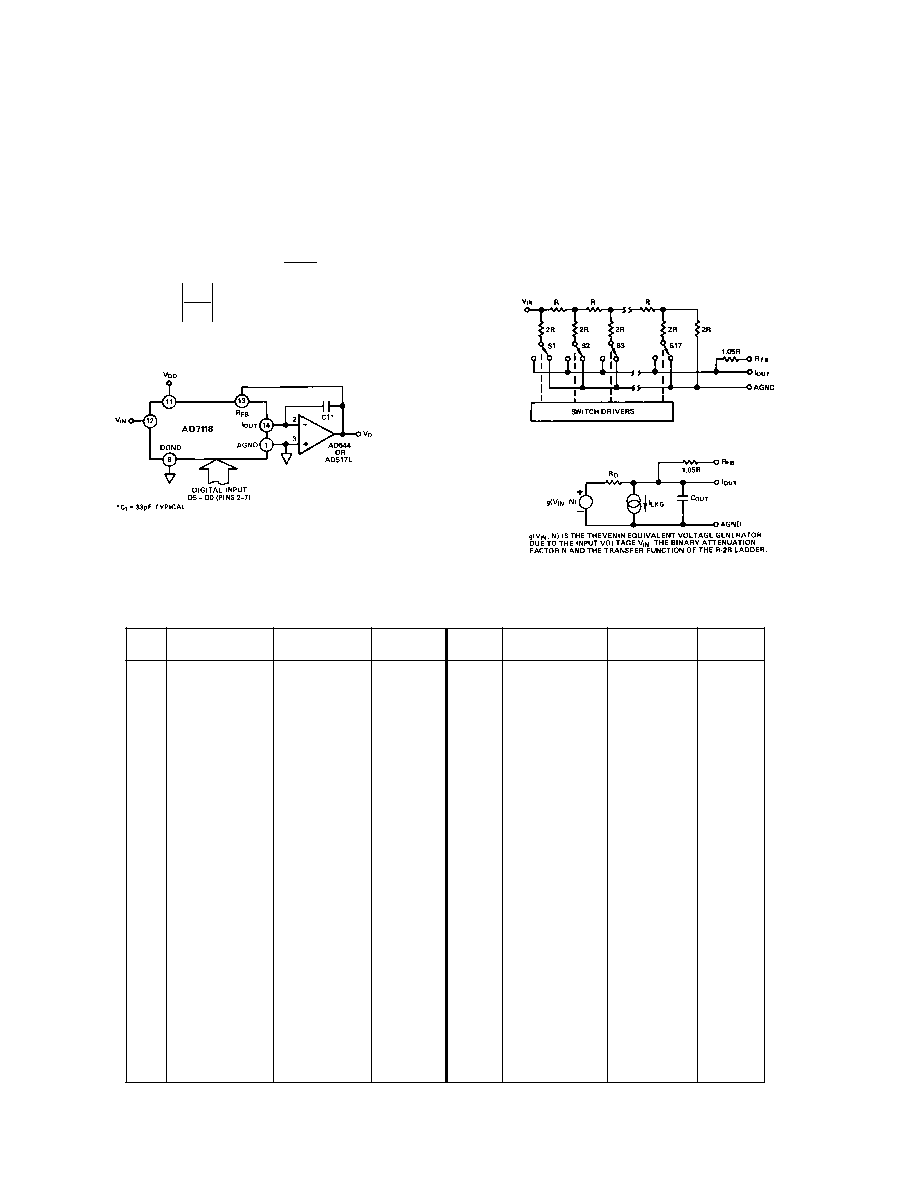
Figure 1. Typical Circuit Configuration
EQUIVALENT CIRCUIT ANALYSIS
Figure 2 shows a simplified circuit of the D/A converter section
of the AD7118 and Figure 3 gives an approximate equivalent
circuit.
The current source I
LEAKAGE
is composed of surface and junc-
tion leakages and as with most semiconductor devices, roughly
doubles every 10
∞
C≠see Figure 10. The resistor R
O
as shown in
Figure 3 is the equivalent output resistance of the device which
varies with input code (excluding all 0's code) from 0.8R to
2R. R is typically 12 k
. C
OUT
is the capacitance due to the
N-channel switches and varies from about 50 pF to 80 pF de-
pending upon the digital input. For further information on
CMOS multiplying D/A converters refer to "Application Guide
to CMOS Multiplying D/A Converters" which is available from
Analog Devices, Publication Number G479≠15≠8/78.
Figure 2. Simplified D/A Circuit of AD7118
Figure 3. Equivalent Analog Output Circuit of AD7118
Digital Input
Attenuation
N
D5
D0
dB
V
OUT
1
N
Digital Input
Attenuation
V
OUT
1
0
0
00 00 00
0
0.0
10.00
31
01 11 11
46.5
0.0473
0
1
00 00 01
0
1.5
8.414
32
10 00 00
48.0
0.0398
0
2
00 00 10
0
3.0
7.079
33
10 00 01
49.5
0.0335
0
3
00 00 11
0
4.5
5.957
34
10 00 10
51.0
0.0282
0
4
00 01 00
0
6.0
5.012
35
10 00 11
52.5
0.0237
0
5
00 01 01
0
7.5
4.217
36
10 01 00
54.0
0.0200
0
6
00 01 10
0
9.0
3.548
37
10 01 01
55.5
0.0168
0
7
00 01 11
10.5
2.985
38
10 01 10
57.0
0.0141
0
8
00 10 00
12.0
2.512
39
10 01 11
58.5
0.0119
0
9
00 10 01
13.5
2.113
40
10 10 00
60.0
0.0100
10
00 10 10
15.0
1.778
41
10 10 01
61.5
0.00841
11
00 10 11
16.5
1.496
42
10 10 10
63.0
0.00708
12
00 11 00
18.0
1.259
43
10 10 11
64.5
0.00596
13
00 11 01
19.5
1.059
44
10 11 00
66.0
0.00501
14
00 11 10
21.0
0.891
45
10 11 01
67.5
0.00422
15
00 11 11
22.5
0.750
46
10 11 10
69.0
0.00355
16
01 00 00
24.0
0.631
47
10 11 11
70.5
0.00299
17
01 00 01
25.5
0.531
48
11 00 00
72.0
0.00251
18
01 00 10
27.0
0.447
49
11 00 01
73.5
0.00211
19
01 00 11
28.5
0.376
50
11 00 10
75.0
0.00178
20
01 01 00
30.0
0.316
51
11 00 11
76.5
0.00150
21
01 01 01
31.5
0.266
52
11 01 00
78.0
0.00126
22
01 01 10
33.0
0.224
53
11 01 01
79.5
0.00106
23
01 01 11
34.5
0.188
54
11 01 10
81.0
0.000891
24
01 10 00
36.0
0.158
55
11 01 11
82.5
0.000750
2
5
01 10 01
37.5
0.133
56
11 10 00
84.0
0.000631
26
01 10 10
39.0
0.112
57
11 10 01
85.5
0.000531
27
01 10 11
40.5
0.0944
58
11 10 10
87.0
0.000447
28
01 11 00
42.0
0.0794
59
11 10 11
88.5
0.000376
29
01 11 01
43.5
0.0668
60
11 11 XX
2
30
01 11 10
45.0
0.0562
NOTES
1
V
IN
= ≠10 V dc
2
X = 1 or 0. Output is fully muted for N
60
3
Monotonic operation is not guaranteed for N = 58, 59
Table I. Ideal Attenuation vs. Input Code

AD7118
REV. A
≠5≠
DYNAMIC PERFORMANCE
The dynamic performance of the AD7118 will depend upon the
gain and phase characteristics of the output amplifier, together
with the optimum choice of PC board layout and decoupling
components. Figure 4 shows a printed circuit layout which
minimizes feedthrough from V
IN
to the output in multiplying
applications. Circuit layout is most important if the optimum
performance of the AD7118 is to be achieved. Most application
problems stem from either poor layout, grounding errors, or in-
appropriate choice of amplifier.
Figure 4. Suggested Layout for AD7118 and Op Amp
It is recommended that when using the AD7118 with a high
speed amplifier, a capacitor C1 be connected in the feedback
path as shown in Figure 1. This capacitor, which should be
between 30 pF and 50 pF, compensates for the phase lag intro-
duced by the output capacitance of the D/A converter. Figures 5
and 6 show the performance of the AD7118 using the AD517, a
fully compensated high gain superbeta amplifier, and the
AD544, a fast FET input amplifier. The performance without
C1 is shown in the middle trace and the response with C1 in
circuit is shown in the bottom trace.
Figure 5. Response of AD7118 with AD517L
Figure 6. Response of AD7118 with AD544S
In conventional CMOS D/A converter design parasitic
capacitance in the N-channel D/A converter switches can give
rise to glitches on the D/A converter output. These glitches re-
sult from digital feedthrough. The AD7118 has been designed
to minimize these glitches as much as possible. It is recom-
mended that for minimum glitch energy the AD7118 be oper-
ated with V
DD
= 5 V. This will reduce the available energy for
coupling across the parasitic capacitance. It should be noted
that the accuracy of the AD7118 improves as V
DD
is increased
(see Figure 8) but the device maintains monotonic behavior to
at least ≠66 dB in the range 5
V
DD
15 volts.
For operation beyond 250 kHz, capacitor C1 may be reduced in
value. This gives an increase in bandwidth at the expense of a
poorer transient response as shown in Figures 6 and 11. In cir-
cuits where C1 is not included the high frequency roll-off point
is primarily determined by the characteristics of the output am-
plifier and not the AD7118.
Feedthrough and absolute accuracy for attenuation levels be-
yond 42 dB are sensitive to output leakage current effects. For
this reason it is recommended that the operating temperature of
the AD7118 be kept as close to 25
∞
C as is practically possible,
particularly where the device's performance at high attenuation
levels is important. A typical plot of leakage current vs. tempera-
ture is shown in Figure 10.
Some solder fluxes and cleaning materials can form slightly con-
ductive films which cause leakage effects between analog input
and output. The user is cautioned to ensure that the manufac-
turing process for circuits using the AD7118 does not allow
such films to form. Otherwise the feedthrough, accuracy and
maximum usable range will be affected.
STATIC ACCURACY PERFORMANCE
The D/A converter section of the AD7118 consists of a 17-bit
R-2R type converter. To obtain optimum static performance at
this level of resolution it is necessary to pay great attention to
amplifier selection, circuit grounding, etc.
Amplifier input bias current results in a dc offset at the output
of the amplifier due to the current flowing through the feedback
resistor R
FB
. It is recommended that an amplifier with an input
bias current of less than 10 nA be used (e.g., AD517 or AD544)
to minimize this offset.
Another error arises from the output amplifier's input offset
voltage. The amplifier is operated with a fixed feedback resis-
tance, but the equivalent source impedance (the AD7118 out-
put impedance) varies as a function of attenuation level. This
has the effect of varying the "noise" gain of the amplifier, thus
creating a varying error due to amplifier offset voltage. To
achieve an output offset error less than one half the smallest step
size, it is recommended that an amplifier with less than 50
µ
V of
input offset be used (such as the AD517 or AD OP07).
If dc accuracy is not critical in the application, it should be
noted that amplifiers with offset voltage up to approximately 2
millivolts can be used. Amplifiers with higher offset voltage may
cause audible "thumps" due to dc output changes.
The AD7118 accuracy is specified and tested using only the
internal feedback resistor. It is not recommended that "gain"
trim resistors be used with the AD7118 because the internal
logic of the circuit executes a proprietary algorithm which ap-
proximates a logarithmic curve with a binary D/A converter: as a
result no single point on the attenuator transfer function can be
guaranteed to lie exactly on the theoretical curve. Any "gain-
error" (i.e., mismatch of R
FB
to the R-2R ladder) that may exist
in the AD7118 D/A converter circuit results in a constant
attenuation error over the whole range. Since the gain error of
CMOS multiplying D/A converters is normally less than 1%,
the accuracy error contribution due to "gain error" effects is
normally less than 0.09 dB.
Applications Information≠

AD7118
REV. A
≠6≠
Figure 7. Digital Threshold & Power Supply Current vs.
Power Supply
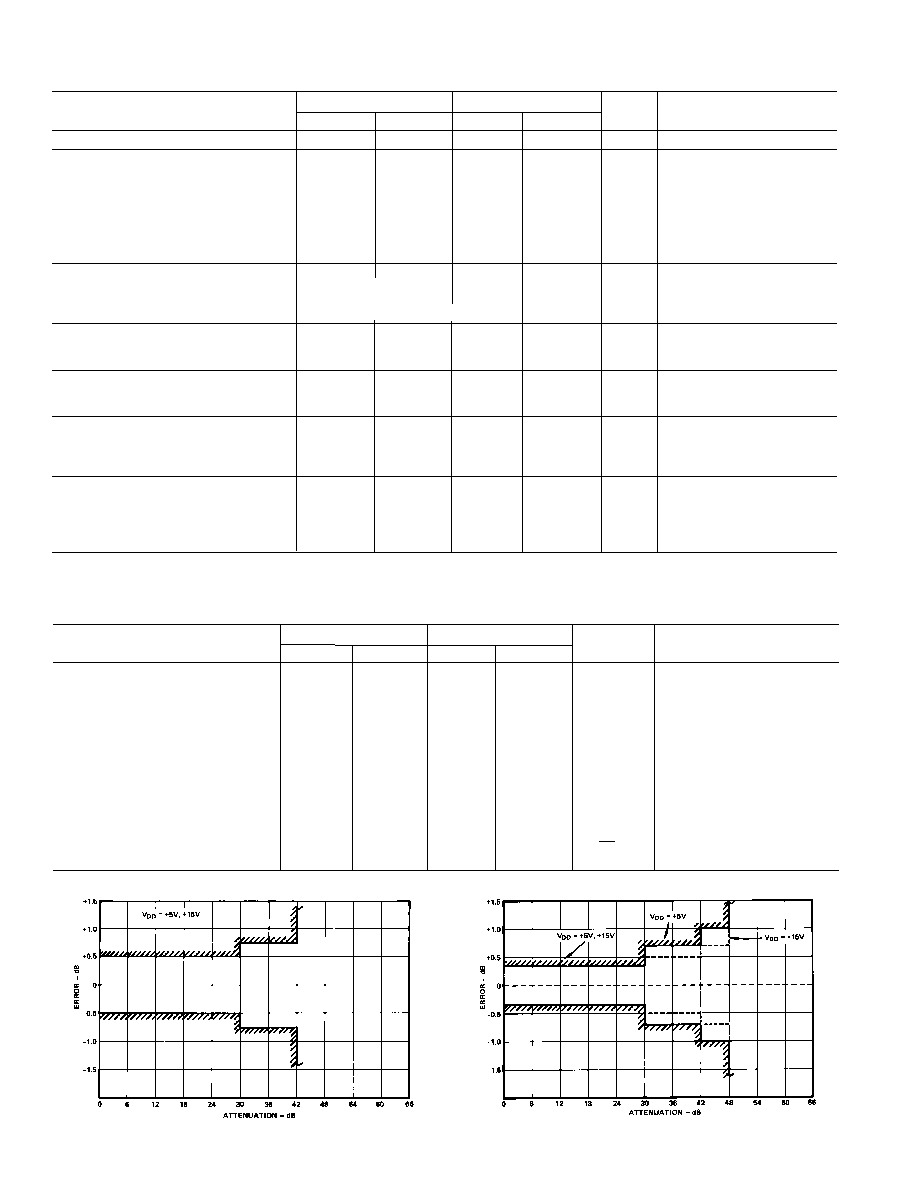
Figure 8. DC Attenuation Error vs. Attenuation & V
DD
Figure 9. DC Attenuation Error vs. Attenuation &
Temperature
Figure 10. Output Leakage Current as Temperature at
V
DD
= 5, 10 and 15 Volts
Figure 11. Frequency Response with AD544 and
AD517 Amplifiers
Figure 12. Distortion vs. Frequency Using AD544
Amplifier
≠Typical Performance Characteristics
C628a≠10≠3/83
PRINTED IN U.S.A.